

Page 1

E2U0034-28-82
¡ Semiconductor MSM7586-01/03
¡ Semiconductor
This version: Aug. 1998
Previous version: Nov. 1996
MSM7586-01/03
p/4 Shift QPSK MODEM/ADPCM CODEC
GENERAL DESCRIPTION
The MSM7586 is a CMOS IC developed for use with digital cordless telephones. The device
provides a p/4 shift QPSK modem function and a CODEC function which performs transcoding
between the voice band analog signal and 32 kbps ADPCM data.
The MSM7586 performs DTMF tone and several types of tone generation, transmit/receive data,
mute and gain control, side-tone pass and its gain control, and VOX function.
FEATURES
(p/4 Shift QPSK Modem Unit)
• 384 kbps transmission speed
• Built-in root Nyquist digital filter for the baseband band limiter
• Built-in D/A converters for the analog outputs of the quadrature signal component I and Q
• The DC offset and gain can be adjusted with respect to the differential I and Q analog outputs
• Completely digitized p/4 shift QPSK demodulator system
(ADPCM CODEC Unit)
• ADPCM system: built-in ITU-T Recommendations G.726 (32kbps, 24 kbps, 16 kbps)
• Transmit/receive full-duplex capability
• PCM interface code format: selectable between m-law and A-law
• Serial ADPCM and PCM transmission rate: 64 kbps to 2,048 kbps
• Transmit/receive mute function; transmit/receive programmable gain setting
• Side tone generator (8-step level adjustment)
• Built-in DTMF tone, ringing tone, and various ringing tone generators
• Built-in VOX function
(Common Unit)
• Operate with a single 3 V power supply (VDD: 2.7 V to 3.6 V)
• Low power consumption
When entire system is operating: 20 mA Typ.
When powered down: 0.02 mA Typ.
• Package:
100-pin plastic TQFP (TQFP100-P-1414-0.50-K) (Product name: MSM7586-01TS-K)
(Product name: MSM7586-03TS-K)
1/42
Page 2
¡ Semiconductor MSM7586-01/03
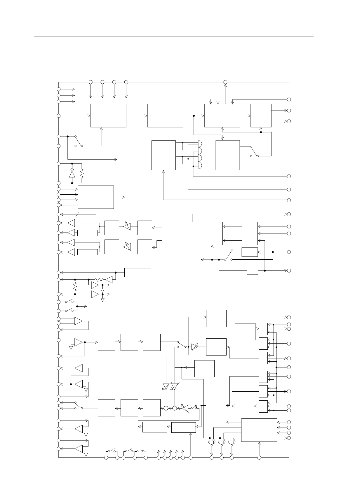
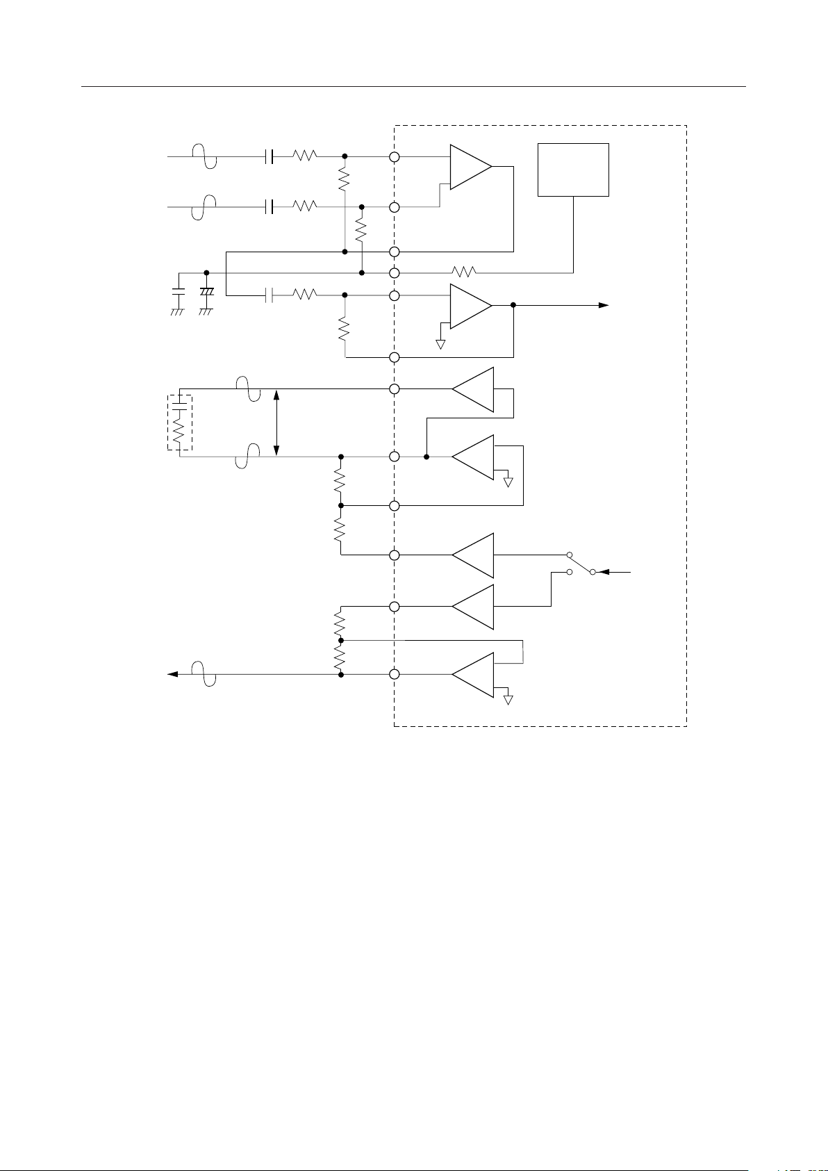
BLOCK DIAGRAM
PDN0
PDN1
PDN2
IFIN
MCK
IFCK
EXCKM
DENM
DINM
DOUTM
R7, R6
R5, R4
SGM
SGCR
SGCT
IO1
IO2
AIN1–
AIN1+
GSX1
AIN2–
GSX2
AOUT+
AOUT–
PWI
VFRO
SAO
AIN3
GSX3
AIN4
GSX4
X2
X1
Q+
Q–
VDAM
Phase
detector
VDDM
DGM
AGM
Delay
detector
SL1
SL2
AFC
RXSC
Decision
AFC
RXD
RXC
SL1
To each block
SL2
MODEM
MCU
To each block
interface
4
I+
I–
+1
–1
+1
–1
DC Adjust
DC Adjust
SW1
SW2
T
CRC4-B5
–
+
–
+
–1
CRC5-B7
CRC5-B6
VDAC
–
+
R
–
+
R
–
+
T
LPF
LPF
R
T
RC
Filter
RC
Filter
CRC5-B5
SW3
CRM1-B7 to B4
ATT
CRM1-B3 to B0
ATT
Receiver
Transmitter
Convertor
Convertor
SW4
VREF
A/D
D/A
CRC5-B4
D/A
D/A
BPF
CRC3-B7 to B5
LPF
Noise
generator
SW5
Root Nyquist LPF
<MODEM Unit>
<CODEC Unit>
CRC4-B6
ATT
+
+
Power detect
CRC2-B6 to B4
ATT
Sign bit
CRC3-B3 to B0
CRC2-B2 to B0
ATT
To each
block
3.84M
DTMF
/Tone
Generator
To D/A
VOICE
DETECT
COMPA
NDER
EXPAN
DER
To each
block
DPLLDEC
CRM0-B6
MAPPING
ADPCM
CODER
ADPCM
DECODER
S/P
PLL
1/10
CODEC
MCU
interface
384k
P
/
S
S
/
P
P
/
S
S
/
P
P
/
S
S
/
P
RPR
RCW
SLS
BSTO
TXD
TXW
TXCI
TXCO
VOXO
XSYNC
IS
PCMSI
PCMSO
BCLK
PCMRI
PCMRO
IR
RSYNC
EXCKC
DENC
DINC
DOUTC
IO3
IO4
IO5
IO6
IO7
VDDC
VDAC
DGC
AGC
PDN3
VOXI
TOUT1
TOUT2
TOUT3
RESET
2/42
Page 3
¡ Semiconductor MSM7586-01/03
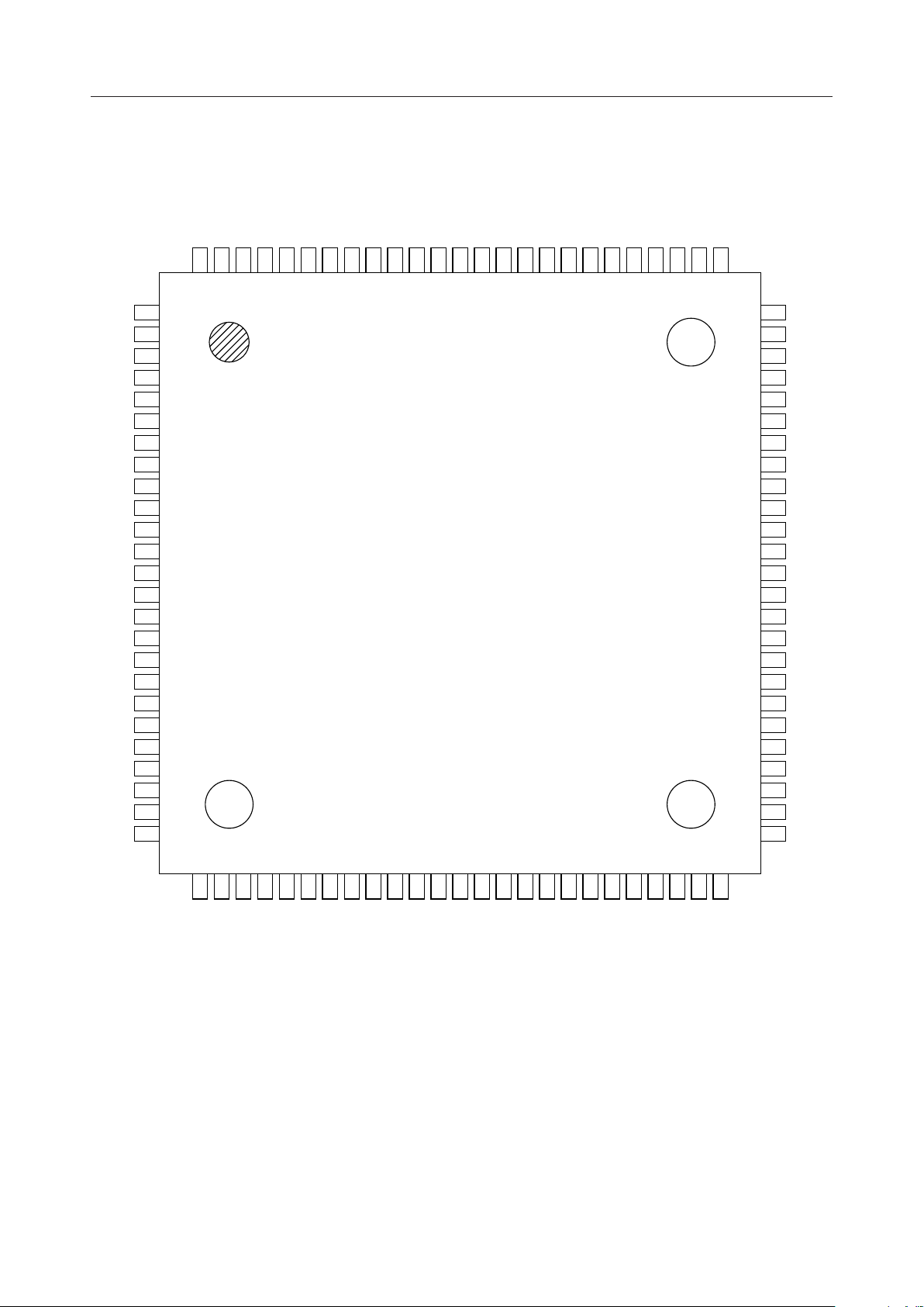
PIN CONFIGURATION (TOP VIEW)
NC
DENM
EXCKM
DOUTM
DINM
78
77
76
100 VDDM
RXSC
SLS
IFINNCX1NCNCX2IFCK
99
98
97
96
95
9493929190
MCK
PDN0
89
PDN1
PDN2NCRCW
88
87
AFC
RPR
RXC
RXD
86
85
84
83
82
81
80
79
VDAM
Q–
Q+
NC
SGM
AGM
AGC
SGCR
SGCT
AIN1+
AIN1–
GSX1
IO5
IO6
IO7
AIN2
GSX2
IO1
IO2
VFRO
PWI
AOUT–
AOUT+
1
2
3
I–
4
I+
5
6
7
8
9
10
11
12
13
14
15
16
17
18
19
20
21
22
23
24
25
75
74
73
72
71
70
69
68
67
66
65
64
63
62
61
60
59
58
57
56
55
54
53
52
51
NC
TXW
TXD
TXCO
TXCI
NC
BSTO
DGM
DGC
R7
R6
R5
R4
NC
BCLK
XSYNC
RSYNC
NC
PCMSO
PCMSI
IS
NC
IR
PCMRO
PCMRI
26
SAO
27
AIN3
28
GSX3
29
VDAC
30
VDDC
31
NC
3233343536
NC
AIN4
GSX4
IO3
IO4
37
NC
38
TOUT1
NC : No connect pin
100-Pin Plastic TQFP
39
TOUT2
40
TOUT3
41
PDN3
42
RESET
43
NC
44
DINC
45
46
EXCKC
DOUTC
47
DENC
48
NC
49
VOXI
50
VOXO
3/42
Page 4

¡ Semiconductor MSM7586-01/03
PIN AND FUNCTIONAL DESCRIPTIONS
(Modem Unit)
TXD
Transmit data input for 384 kbps.
TXCI
Transmit clock input.
When the control register CRM0 - B6 is "0", a 384 kHz clock pulse synchronous with TXD should
be input to this pin. This clock pulse should be continuous because this device use APLL to
generate an internal clock pulse.
When CRM0 - B6 is "1", a 3.84 MHz clock pulse should be input to this pin. When the 3.84 MHz
clock pulse is applied to TXCL, TXCO outputs a 384 kHz clock pulse, which is generated by
dividing the TXCL input by 10. The transmit data, synchronous to the 384 kHz clock pulse,
should be input to the TXD. In this case the devices do not use APLL, and the 3.84 MHz clock pulse
need not be continuous. (Refer to Fig. 1.)
TXCO
Transmit clock output.
When CRM0 - B6 is "0", TXCO outputs the 384 kHz clock pulse (APLL output) for monitoring
purposes. When CRM0 - B6 is "1", this pin outputs a 384 kHz clock pulse generated by dividing
the TXCI input by 10. (Refer to Fig. 1.)
TXW
Transmit data window signal input.
The transmit timing signal for the burst data is input to this pin. If TXW is "1", the modulation
data is output. (Refer to Fig. 1)
4/42
Page 5
¡ Semiconductor MSM7586-01/03
(1) CRM0 – B6 = "0"
TXD
TXCI
(384 kHz)
TXW
TXCO
(384 kHz)
I, Q
D0 D1 D2 D3 D4 D5 D6 D7 D8 D9 D10 D11 D12 D13 Dn-1 D
n
(2) CRM0 – B6 = "1"
TXD
TXCI
(3.84 MHz)
TXW
TXCO
(3.84 kHz)
I, Q
D0 D1 D2 D3 D4 D5 D6 D7 D8 D9 D10 D11 D12 D13 Dn-1 D
Ramp rise-up
Delay of 6.25 symbols Delay of 6.25 symbols
Delay of 6.25 symbols Delay of 6.25 symbols
2 symbols
n
Ramp rise-up
2 symbols
Figure 1 Transmit Timing Diagram
Ramp
Fall-down
2 symbols
Ramp
Fall-down
2 symbols
5/42
Page 6

¡ Semiconductor MSM7586-01/03
BSTO
BSTO is the modulator side burst window output.
The burst position of the I and Q baseband modulator output is output.
I+, I–
Quadrature modulation signal I Component differential analog output.
Their output levels are 500 mVpp (when TXD = "0": 360 mVpp typ.) with 1.6 Vdc as the center
value. The output pin load conditions are: R ≥ 10 kW, C £ 20 pF. The gain of these pins can be
adjusted using the control register CRM1 - B7 to B4, and the offset voltage at the I– pin can be
adjusted using CRM3 - B7 to B3.
Q+, Q–
Quadrature modulation signal Q component differential analog outputs.
Their output levels are 500 mVpp (when TXD = "0": 360 mVpp typ.) with 1.6 Vdc as the center
value. The output pin load conditions are: R ≥ 10 kW, C £ 20 pF. The gain of these pins can be
adjusted using the control register CRM1 - B3 to B0, and the offset voltage at the Q– pin can be
adjusted by using CRM4 - B7 to B3.
SGM
Internal reference voltage output.
The output voltage value is approximately 2.0 V. Insert a bypass capacitor between this pin and
the AGM pin. During power down, this output is at 0 V.
The external SG voltage if necessary should be used via a buffer.
6/42
Page 7
¡ Semiconductor MSM7586-01/03
PDN0, PDN1, PDN2
Various power down control.
PDN0 controls the standby mode/communication mode; PDN1 controls the modulator unit;
and PDN2 controls the demodulator unit. Refer to Table 1 for details.
The control register reset input width should be 200ns or more.
Table 1: Description of Modem Power Down Control
Standby
Mode
Communication
Mode
PDN0
PDN2 PDN1
0 0/1 1 Mode A
0 0 0 Mode BEntire system is powered down. The control register is not reset.
0 1 0 Mode CModulator unit is powered off. (VREF and PLL also powered off.)
1 0 0 Mode D
1 0 1 Mode EModulator unit is powered on.
1 1 0 Mode FModulator unit is powered off. (VREF and PLL are powered off.)
1 1 1 Mode G
Entire system is powered down. The control register is reset.
Demodulator unit is powered on.
Modulator unit is powered off. (VREF and PLL are powered on.)
I and Q outputs are in a high impedance state.
Only the demodulator clock regenerator unit is powered on.
Only the demodulator clock regenerator unit is powered on.
I and Q outputs are in a high impedance state.
Demodulator unit is powered on.
Modulator unit is powered on.
Demodulator unit is powered on.
Operation State
Mode Name
7/42
Page 8
¡ Semiconductor MSM7586-01/03
VDDM, VDAM
+3 V power supply for the modem unit.
Supplied to the digital circuits through the VDDM pin and to the analog circuits through the
VDAM pin. VDDM and VDAM, and VDDC and VDAC should be connected as close as possible
on the PC board.
DGM, AGM
Ground pins for the modem unit.
DGM is the ground pin of the digital system, and AGM is the ground pin of the analog system.
Since DGM and AGM are isolated inside the IC, connect them as close as possible on the circuit
board.
MCK
Master clock input.
The clock frequency is 19.2 MHz.
IFIN
Modulated signal input for the demodulator block.
Select the IF frequency can be selected from 1.2 MHz, 10.7 MHz, 10.75 MHz, and 10.8 MHz, based
on CRM0 - B4 and B3.
IFCK
Clock frequency 19.0222 MHz input for demodulator block IF frequencies of 10.7 MHz.
If the IF frequency is 1.2 MHz or 10.8 MHz, set this pin to "0" or "1". (Refer to Fig. 2.)
X1, X2
Crystal oscillator connection pins.
When supplying a 19.0222 MHz clock to IFCK, use these pins. (Refer to Fig. 2.)
When IFIN = 10.7 MHz
MSM7586
When IFIN = 1.2 MHz or 10.8 MHz
MSM7586
X1 X2 IFCK
19.0222 MHz
Figure 2 How to Use IFCK, X1, and X2
X1 X2 IFCK
8/42
Page 9
¡ Semiconductor MSM7586-01/03
RXD, RXC, RXSC
Receive data and receive clock outputs.
When the modem unit is powered on, RXD, RXC and RXSC are selected based on SLS as shown
in Figure 3. These outputs are used by the clock regenerator circuit.
RXD
RXC
RXSC
SLS
1 Symbol
The regenerated data and clock are
selected asynchronously by the SLS signal.
Figure 3 Timing Diagram of RXD, RXC, and RXSC
SLS
Receive side operation slot selection signal.
This device has two clock regenerator circuits and two AFC data memory registers. If SLS is "0",
slot 1 is selected, if SLS is "1", slot 2 is selected.
RPR
High-speed phase clock control signal input for the clock recovery circuit.
If this pin is at "0", the circuit is always in the low-speed phase clock mode. If this pin is at "1",
the clock recovery circuit enters the high-speed phase clock mode. When the phase difference
is less than a defined value, the circuit shifts to the low-speed phase clock mode automatically.
9/42
Page 10
¡ Semiconductor MSM7586-01/03
AFC
AFC operation range specification signal input.
As shown in Fig. 4, the AFC information is reset when both AFC and RPR are set to "1". AFC
operation starts after a fixed number of clock cycles and the AFC information is reset. If RPR is
set to "1", an average number of times that AFC turns on is low. If RPR is "0", AFC is high. If AFC
is "0", frequency error is not calculated, but the frequency is corrected using an error that is held.
RCW
Clock recovery circuit operation ON/OFF control signal input.
If RCW this pin is "0", DPLL does not make any phase corrections.
(CASE1)
AFC
RPR
Average number of times
AFC is high.
AFC information
is maintained.
(CASE2)
AFC information
is reset.
Average
number of times
AFC is low.
AFC
RPR
The clock recovery circuit
starts with the previous
AFC information.
"0"
Average number of times
AFC is high.
AFC information
is maintained.
Figure 4 AFC Control Timing Diagram
DENM , EXCKM, DINM, DOUTM
Serial control ports for the microprocessor interface.
The device contains a 6-byte control register (CRM0 - 5). An external CPU uses these pins to read
data from and write data to the control register. DENM is the "Enable" signal input pin. EXCKM
is a data shift clock pulse input pin. DINM is an address and data input pin. DOUTM is a data
output pin. Figure 5 shows input/output timing diagram.
10/42
Page 11
¡ Semiconductor MSM7586-01/03
,
DENM
EXCKM
W
A2
DINM
A1 A0 B7 B6 B5 B4 B3 B2 B1 B0
DOUTM
DENM
EXCKM
DINM
DOUTM
High Impedance
R A2A1A0
Figure 5 Modem Unit MCU Interface I/O Timing
The register map is shown below.
Table 2: Modem Unit Control Register (CRM0 to 5) Map
Register
Name
CRM0
CRM1
Address
A2 A1 A0
000
001
B7 B6 B5 B4 B3 B2 B1 B0
—
Ich
GAIN3
GAIN2
High Impedance
(a) Write Data Timing Diagram
B7 B6 B5 B4 B3 B2 B1 B0
(b) Read Data Timing Diagram
Data Description
TXC
SEL
Ich
MOD
OFF
Ich
GAIN1
IFSEL1 IFSEL0 — TEST1 TEST0
Ich
GAIN0
Qch
GAIN3
Qch
GAIN2
Qch
GAIN1
R/W
R/W
Qch
R/W
GAIN0
CRM2
CRM3
CRM4
CRM5
010
011
100
101
R7 R6 R5 R4 — — — —
Ich
Offset4
Qch
Offset4
ICT5 ICT4 ICT3 ICT2
Ich
Offset3
Qch
Offset3
Ich
Offset2
Qch
Offset2
Ich
Offset1
Qch
Offset1
Ich
Offset0
Qch
Offset0
LOCAL
INV1
R/W: Read/Write enable R: Read-only register
R7, R6, R5, R4
These are the control register data output pins.
These output the data CRM2 - B7, B6, B5, and B4, respectively.
———
———
LOCAL
INV0
ICT1 ICT0
R/W
R/W
R/W
R/W
11/42
Page 12

¡ Semiconductor MSM7586-01/03
(CODEC Unit)
AIN1+, AIN1-, AIN2, GSX1, GSX2
The transmit analog input and the output for transmit gain adjustment.
The pin AIN1–(AIN2) connects to the inverting input of the internal transmit amplifier, and the
pin AIN1+ connects to the non-inverting input of the internal transmit amplifier. The pin GSX1
(GSX2) connects to output of the internal transmit amplifier. See Fig. 6 for gain adjustment.
VFRO, AOUT+, AOUT-, PWI
Used for the receive analog output and the output for receive gain adjustment.
VFRO is an output of the receive filter. AOUT+ and AOUT– are differential analog signal outputs
which can directly drive ZL = 350 W+120 nF or the 1.2 kW load. See Fig. 6 for gain adjustment.
However, these outputs are in high impedance state during power down.
SAO, AIN3, AIN4, GSX3, GSX4
Input pins for the internal operational amp.
Refer to Fig.␣ 6 for connection information. However, these output pins are in the high impedance
state during power down.
12/42
Page 13
¡ Semiconductor MSM7586-01/03
Vi
Differential analog input signal
C1
C1 R1
+
–
= 120 nF
Z
L
+ 350 W
Transmit gain : (V
= (R2/R1) ¥ (R4/R3)
Receive gain : (VO/V
= 2 ¥ (R6/R5)
C2
GSX2
R1
R2
R3
R4
Analog output signal
Vo
/Vi)
VFRO
)
R6
R5
R2
AIN1–
AIN1+
GSX1
SGCT
AIN2
GSX2
AOUT+
AOUT–
VFRO
–
+
Reference
voltage
generator
–
+
to ENCODER
–1
–
+
from
+1
DECODER
Sounder output signal
Sounder output gain : (V
= V
¥ (R8/R7)
SAO
Figure 6 CODEC Unit Analog Interface
GSX3
R7
R8
SAO
AIN3
GSX3
+1
–
+
)
13/42
Page 14

¡ Semiconductor MSM7586-01/03
IO1 to IO7
I/O pins of the internal analog switch.
Refer to the control register description table (CRC5) and the block diagram for connection
information and control methods.
TOUT1 to TOUT3
Sign bit output pins of the tone generator.
Output control of each pin is performed by the control register. Refer to the control register
description table (CRC5) and the block diagram for connection information and control methods.
SGCT, SGCR
Output pins of the CODEC unit analog signal ground voltage.
SGCT outputs the analog signal ground voltage of the transmit system, and SGCR outputs the
same for the receive system. The output voltage value is approximately 1.4 V. Connect 10 mF and
0.1 mF bypass capacitors (ceramic type) between these pins and the AGC pin. During power
down, the output changes to 0 V. The external SG voltage if necessary should be used via a buffer.
VDDC, VDAC
CODEC unit +3 V power supply.
VDDC is supplied to the digital system power supply, and VDAC is supplied to the analog
system power supply. VDDC and VDAC, and VDDM and VDAM must be connected as possible
on the PC board.
DGC, AGC
CODEC unit ground.
DGC is the digital system ground pin, and AGC is the analog system ground pin. Since DGC and
AGC are unconnected in the device, place them as close together as possible on the circuit board.
PDN3
CODEC unit power-down control input.
The CODEC unit changes to the power - down state when set to a digital "0." Since the powerdown control is handled by an OR with control register CRC0 - B5, set CRC0 - B5 to digital "0"
when using this pin.
RESET
Reset control input pin of the CODEC unit control register.
When set to digital "0," each bit of the control register is reset. During normal operation, set this
pin to digital "1." A more than 200ns reset signal should be input.
14/42
Page 15

¡ Semiconductor MSM7586-01/03
PCMSO
Transmit PCM data output.
This PCM output signal is output from MSB synchronous with the rising edge of BCLK and
XSYNC.
PCMSI
Transmit PCM data input.
This signal is converted to the ADPCM data. The PCM signal is shifted on the falling edge of
BCLK. Normally, this pin is connected to PCMSO.
PCMRO
Receive PCM data output.
The PCM signal is the output signal after ADPCM decoder processing. This signal is serially
output from the MSB synchronous with the rising edge of BCLK and RSYNC.
PCMRI
Receive PCM data input.
The PCM input signal is shifted on the falling edge of BCLK and input from MSB. Normally, this
pin is connected to PCMRO.
IS
Transmit ADPCM signal output.
This signal is the output signal after ADPCM encoding, and is serially output from MSB
synchronous with the rising edge of BCLK and XSYNC. This pin is an open drain output which
remains in a high impedence state during power-down, and requires a pull-up resistor.
IR
Receive ADPCM signal input.
Input data is shifted serially from MSB on the falling edge of BCLK synchronous with RSYNC.
BCLK
Shift clock input for the PCM data (PCMSO, PCMSI, PCMRO, PCMRI) and the ADPCM data(IS,
IR) .
The frequency ranges from 64 kHz to 2048 kHz.
XSYNC
Transmit PCM and ADPCM data 8 kHz synchronous signal input.
This signal should be synchronous with BCLK. XSYNC is used for indicating MSB of the transmit
serial PCM and ADPCM data stream.
RSYNC
Receive PCM and ADPCM data 8 kHz synchronous signal input.
This signal should be synchronous with BCLK signal. RSYNC is used for indicating MSB of the
receive serial PCM and ADPCM data stream.
15/42
Page 16

¡ Semiconductor MSM7586-01/03
VOXO
Transmit VOX function signal output.
VOX function is used to recognize the presence or absence of the transmit voice signal by
detecting the signal energy. "H" and "L" levels on this pin correspond to the presence and the
absence, respectively. This result also appears at the register data CRC7 - B7. The signal energy
detect threshold is set by the control register data CRC6 - B6, B5.
VOXI
Signal input for receive VOX function.
The "H" level on VOXI indicates the presence of voice signal, the decoder block processes normal
receive signal, and the voice signal appears at analog output pins . The "L" level indicates the
absence of voice signal, the background noise generated in this device is transferred to the analog
output pins. The background noise amplitude is set by the control register CRC6. Because this
signal is ORed with the register data CRC6 - B3, the control register data CRC6 - B3 should be set
to digital "0".
Input voice signal
GSX2
pin
VOXO pin
VOXI pin
Regenerated voice
VFRO
pin
Voice Silience Voice
Voice detection time
Tvxon
(a) Transmission Side VOX Function Timing Diagram
Voice Silience Voice
Regenerated voice signal
generation time
Silence detection time
(Hangover time) Tvxoff
Internal background
noise generation time
(b) Receive Side VOX Function Timing Diagram
Note: The VOXO and VOXI pin function are enabled when CRC6 - B7 is set to "1".
Figure 7 VOX Function
16/42
Page 17

¡ Semiconductor MSM7586-01/03
,
DENC, EXCKC, DINC, DOUTC
Serial control ports for MCU interface.
Reading and writing data are performed by an external MCU through these pins. The 8-byte
control registers (CRC0 - 7) are provided for the CODEC unit in this device. DENC is the "Enable"
control signal input, EXCKC is the data shift clock input, DINC is the address and data input, and
DOUTC is the data output. Figure 8 shows input/output timing diagram.
DENC
EXCKC
W
A2
DINC
A1 A0 B7 B6 B5 B4 B3 B2 B1 B0
DOUTC
DENC
EXCKC
DINC
DOUTC
High Impedance
R A2A1A0
Figure 8 CODEC Unit MCU Interface I/O Timing
The register map is shown below.
Table 3: CODEC Unit Control Register (CRC0 to 7) Map
Register
Name
CRC0
CRC1
CRC2
CRC3
CRC4
CRC5
CRC6
CRC7
Address
A2 A1 A0
000
001
010
011
100
101
110
111
B7 B6 B5 B4 B3 B2 B1 B0
A/m
SEL
MODE1 MODE0
TX
ON/OFFTXGAIN2TXGAIN1TXGAIN0RXON/OFFRXGAIN2RXGAIN1RXGAIN0
Side Tone
GAIN2
DTMF/
OTHERS
SEL
SW1
CONT
VOX
ON/OFFONLVL1
VOX
OUT
Side Tone
GAIN1
TX NOISE
High Impedance
(a) Write Data Timing Diagram
B7 B6 B5 B4 B3 B2 B1 B0
(b) Read Data Timing Diagram
Data Description
—
TONE
SEND
SW2
CONT
LVL1
PDN
ALL
TX
RESETRXRESETTXMUTERXMUTE
Side Tone
GAIN0
SAO/
VFRO
SW3
CONT
ON
LVL0
TX NOISE
LVL0
——
TONE
ON/OFF
TONE4 TONE3 TONE2 TONE1 TONE0
SW4/5
CONT
OFF
TIME
—————
TONE
GAIN3
—
VOX
IN
——
—
TONE
GAIN2
TOUT3
CONT
RX NOISE
LEVEL SEL
TONE
GAIN1
TOUT2
CONT
RX NOISE
LVL1
R/W
PDN
R/W
SAO/AOUT
RX
R/W
PAD
R/W
TONE
R/W
GAIN0
R/W
TOUT1
R/W
CONT
RX NOISE
R/W
LVL0
R
R/W: Read/Write enable R: Read-only register
17/42
Page 18

¡ Semiconductor MSM7586-01/03
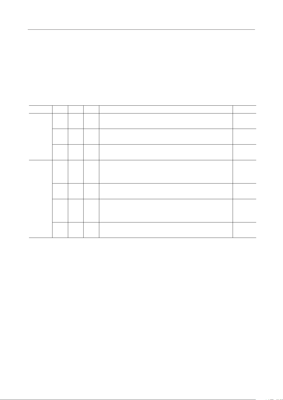
ABSOLUTE MAXIMUM RATINGS
Parameter
Power Supply Voltage
Analog Input Voltage
Digital Input Voltage
Storage Temperature
Symbol
V
DD
V
AIN
V
DIN
T
STG
Condition
—
—
—
—
RECOMMENDED OPERATING CONDITIONS
Parameter
Power Supply Voltage
Operating Temperature
Input High Voltage
Input Low Voltage
Digital Input Rise Time
Digital Input Fall Time
Digital Output Load
Bypass Capacitor for SG
Master Clock Frequency
Master Clock Duty Ratio
Modulator Side Input
Frequency
Demodulator Side
Input Frequency
Clock Duty Ratio
IF Input Duty Ratio
Modem Unit
Transmit Sync Pulse
Setting Time
Bit Clock Frequency
Synchronous Signal Frequency
Clock Duty Ratio
Transmit Sync Pulse Setting Time
Receive Sync Pulse Setting Time
CODEC Unit
Synchronous Signal Width
PCM, ADPCM Set-up Time
PCM, ADPCM Hold Time
Symbol
V
DD
Ta
V
IH
V
IL
t
Ir
t
If
R
DL
C
DL
C
SG
F
MCK
D
MCK
F
TXC1
F
TXC2
F
IFCK1
F
IFCK2
D
CKM
D
CIF
t
XSM, tSXM
t
SDM, tDHM
F
BCK
F
SYNC
D
CKC
t
t
XSC,
SXC
t
t
RSC,
SRC
t
WSC
t
DSC
t
DHC
Conditon
Voltage must be fixed
—
Input pins fully digital
Input pins fully digital
Input pins fully digital
Input pins fully digital
IS (Pull-up resistance)
Input pins fully digital
Between SGM and AGM,
and between SGCT/R and AGC
MCK
MCK
TXCI (When CRM0 - B6 = "0")
TXCI (When CRM0 - B6 = "1")
IFCK
IFCK
(When
(When
IFIN = 10.7 MHz)
IFIN = 10.75 MHz)
IFCK, TXCI, EXCKM
IFIN
TXCI´TXW
TXCI´TXD
BCLK
XSYNC, RSYNC
BCLK, EXCKC
BCLK´XSYNC
BCLK´RSYNC
XSYNC, RSYNC
—
—
Rating
–0.3 to +5
–0.3 to V
–0.3 to V
DD
DD
+ 0.3
+ 0.3
–55 to +150
(VDD = 2.7 V to 3.6 V, Ta = –25°C to +70°C)
Min. Typ. Max. Unit
2.7 — 3.6 V
–25 +25 +70 °C
0.45 ¥
V
DD
—
V
DD
0.16 ¥
—
—
—
—
—
—
19.2
50
384
3.84
19.0222
19.1111
50
50
—
V
DD
+0.01% MHz
Fig.9
0
—50ns
—50ns
500 — W
— 100 pF
10 + 0.1 — mF
–0.01%
40 60 %
— — kHz
— — MHz
— — MHz
— — MHz
40 60 %
45 55 %
200 — ns
200 — ns—
64 2048 kHz —
— — kHz8.0
40 60 %50
100 — ns—
100 — ns—
Fig.12
1 BCLK 100 ms—
100 — ns—
100 — ns—
Unit
V
V
V
°C
V
V
18/42
Page 19

¡ Semiconductor MSM7586-01/03
ELECTRICAL CHARACTERISTICS
DC Characteristics
=
(V
2.7 V to 3.6 V, Ta = –25°C to +70°C)
DD
Parameter
Power Supply Current
(Modem Unit)
* When CODEC Unit is in a
Power Down State
Power Supply Current (CODEC Unit)
* When Modem Unit is in a Power
Down State
Symbol
I
DD1
I
DD2
I
DD3
I
DD4
I
DD5
I
DD6
I
DD7
I
DD8
I
DD9
Condition
Mode A, Mode B (When V
Mode C (
Mode D (
Mode E (
Mode F (
Mode G (
When V
When V
When V
When V
When V
DD
DD
DD
DD
DD
= 3.0 V)
DD
= 3.0 V
) — 5.5 11.0 mA
= 3.0 V
) — 5.5 11.0 mA
= 3.0 V
) — 11.5 23.0 mA
= 3.0 V
) — 9.5 19.0 mA
= 3.0 V
) — 14.0 28.0 mA
When operating *
(When no signal, and VDD = 3.0 V)
When powered down
(When V
= 3.0 V)
DD
Min.
Typ.
Max.
— 0.02 0.1 mA
— 8.0 16.0 mA
—
—
12.0
0.02
19.0
0.1
Unit
mA
mA
Input Leakage Current
Output High Voltage
Output Low Voltage
Output Leakage Current
Input Capacitance
*I
applies when CRC0 - B0 = "0" and CRC4 - B5 = "0"; I
DD7
times.
=
V
I
IH
I
IL
V
OH
V
OL
V
I
DD
=
V
0 V
I
=
0.4 mA
I
OH
=
I
1 mA—V
OH
= –1.2 mA
I
OL
(IS pin is 500 W pull-up)
I
IS pin
O
C
IN
—
—
0.5 ¥ V
0.8 ¥ V
0
—
DD
DD
—
—
—
0.2
—
2.0
0.5
V
0.4
10
DD
DD
mA
mA
V
V
V
mA
— —5—pF
applies when operating at other
DD8
19/42
Page 20

¡ Semiconductor MSM7586-01/03
Analog Interface Characteristics (Modem Unit)
(V
= 2.7 V to 3.6 V, Ta = –25°C to +70°C)
DD
Parameter
Output Resistance Load
Output Capacitance Load C
Output DC Voltage Level V
Output AC Voltage Level
Offset Voltage Difference V
Modulator D/A
Conversion Sampling Frequency
Modulator D/A
Conversion Offset Frequency
Output DC Voltage Adjustment Level Range
Output AC Voltage Adjustment Level Range
Out-of-band Spectrum
Modulation Accuracy
Demodulator Side IF Input Level I
IFIN Input Impedance R
SGM Output Voltage V
SGM Output Impedance R
Master Clock External Input Level
X1 Input Impedande RX1 — 2.0 — MW
X1 Input Capacitance CX1 — 10 — pF
Symbol
R
LIQ
LIQ
DCM
I+, I–, Q+, Q–
I+, I–, Q+, Q– — — 20 pF
I+, I–, Q+, Q–
Condition
(TXW = 0)
Min.
10
Typ.
—
Max.—Unit
1.55 1.6 1.65 V
I+, I–, Q+, Q–
V
ACM
(For TXD = 0 continuous input)
340 360 380 mV
Difference among
OFF
I+, I–, Q+ and Q–
F
SDA
F
CDA
D
CVL
A
CVL
—
—
–20 — +20 mV
— 1.92 — MHz—
— 380 — kHz—
— ±45 — mV
—±4—%
P600 600 kHz detuning (continuous) 60 — — dB
P900 900 kHz detuning (continuous) 65 — — dB
E
VM
IFIN input level 0.4 — V
FV
DC impedance
IF
SGM
SGM
—
—
—
— 1.0 3.0
DD
—20—kW
— 2.0 — V
— 1.5 — kW
X1 input level
I
X11
(When CRM5 – B1 = "0")
1.5 — V
DD
X1 input level
I
X12
(When CRM5 – B1 = "1")
0.7 — V
DD
—
—
kW
%
rms
V
PP
V
PP
V
PP
PP
20/42
Page 21

¡ Semiconductor MSM7586-01/03
Digital Interface Characteristics (Modem Unit)
= 2.7 V to 3.6 V, Ta = –25°C to +70°C)
(V
DD
Parameter
Transmit
Digital I/O Setting Time
Receive Digital I/O Setting Time
Serial Port
Digital I/O Setting Time
Symbol
t
XDM1,2
t
XDM3,4
t
RDM1,2
t
M1
t
M2
t
M3
t
M4
t
M5
t
M6
t
M7
t
M8
t
M9
t
M10
t
M11
t
M12
Condition
C load = 50 pF
Reference
Fig. 9
C load = 50 pF Fig. 10 0 — 200 ns
C load = 50 pF Fig. 11
EXCK Clock Frequency Feckm EXCKM — — — 10 MHz
Min.
0
Typ.
—
Max.
200
Unit
ns
0 — 400 ns
50——ns
50——ns
50——ns
50——ns
100 — — ns
50——ns
50——ns
0 — 100 ns
50——ns
50——ns
0 — 50 ns
200 — — ns
21/42
Page 22

¡ Semiconductor MSM7586-01/03
Analog Interface Characteristics (CODEC Unit)
(V
= 2.7 V to 3.6 V, Ta = –25°C to +70°C)
DD
Parameter
Symbol
Input Resistance
Output Resistance Load
Output Capacitance Load
Output Voltage Level (*1)
Offset Voltage
SGCT, SGCR Output Voltage V
SGCT Output Impedance R
SGCR Output Impedance R
SGCT Rise Time T
SGCR Rise Time T
Analog Switch OFF Resistance R
Analog Switch ON Resistance R
R
R
R
R
C
C
C
V
V
V
V
OFC1
V
OFC2
SGCT
SGCR
SGCT
SGCR
SWof
SWon
Condition
Min.
Typ.
AIN+, AIN–, AIN2, PWI,
INC
AIN3, AIN4
GSX1, GSX2, VFRO, SAO
LC1
AOUT+, AOUT–, GSX4
LC2
GSX3 150 — — W
LC3
GSX1, GSX2, VFRO, SAO
LC1
AOUT+, AOUT–, GSX4
LC2
GSX3 — — 100 pF
LC3
10
20
1.2 — — kW
—
— — 100 pF
—
—
—
GSX1, GSX2, VFRO,
OC1
SAO(RL = 20 kW)
—
—
AOUT+, AOUT–, GSX4
OC2
(RL = 1.2 kW)
GSX3(RL = 150 W)
OC3
VFRO, SAO
— — 1.3 V
— — 1.3 V
–100
—
GSX1, GSX2, AOUT+,
–20 — +20 mV
AOUT–, GSX3, GSX4
SGC
— 1.4 — VSGCT, SGCR
—4080kWSGCT
—4 8kWSGCR
For the Recommended Circuit
(Rise time to 90% of max. level)
— 600 — ms
For the Recommended Circuit
(Rise time to 90% of max. level)
—15—ms
50——MWSW1 to SW5
100 — 400 WSW1 to SW5
Max.
—
—
100
1.3
+100
Unit
MW
kW
pF
V
PP
PP
PP
mV
Note : *1 –7.7 dBm (600 W) = 0 dBm0, +3.14 dBm0 = 1.30 VPP (A-law)
–7.7 dBm (600 W) = 0 dBm0, +3.17 dBm0 = 1.30 VPP (m-law)
22/42
Page 23

¡ Semiconductor MSM7586-01/03
Digital Interface Characteristics (CODEC Unit)
(V
= 2.7 V to 3.6 V, Ta = –25°C to +70°C)
DD
Parameter
Digital Output Delay Time
PCM, ADPCM Interface
Serial Port Digital I/O
Timing Characteristics
Symbol
t
SDXC, tSDRC
t
XDC1, tRDC1
t
XDC2, tRDC2
t
XDC3, tRDC3
t
C1
t
C2
t
C3
t
C4
t
C5
t
C6
t
C7
t
C8
t
C9
t
C10
t
C11
t
C12
Condition
Reference
1 LSTTL + 100 pF
pull-up : 500 W
Items in parenthesis
Fig. 12
( ) mean C load = 10 pF,
and the pull-up £ 2 kW
C load = 50 pF Fig. 13
EXCK Clock Frequency Feckc EXCKC — — — 10 MHz
Min.
0
0— ns
0— ns
0— ns
Typ.
—
Max.
200 (100)
200 (100)
200 (100)
200 (100)
Unit
ns
50 — — ns
50 — — ns
50 — — ns
50 — — ns
100 — — ns
50 — — ns
50 — — ns
0 — 100 ns
50 — — ns
50 — — ns
0 — 50 ns
200 — — ns
23/42
Page 24

¡ Semiconductor MSM7586-01/03
AC Characteristics (CODEC Unit)
Parameter
Transmit Frequency
Response
Receive Frequency
Response
Transmit Signal to
Distortion Ratio (*2)
Receive Signal to
Distortion Ratio (*2)
Transmit Gain
Tracking
Receive Gain
Tracking
Symbol
Frequency (Hz)
L
L
L
L
L
L
L
L
L
L
L
OSS
OSS
OSS
OSS
OSS
OSS
OSS
OSS
OSS
OSS
OSS
T1
T2
T3
T4
T5
T6
R1
R2
R3
R4
R5
0 to 60
300 to 3 k
1020
3300
3400
3968.75
0 to 3000
1020
3300
3400
3968.75
SD T1 35 —
SD T2 35 —
SD T3 35 —
1020
SD T4 28 —
SD T5 23 —
SD R1 —
SD R2 —
SD R3 —
1020
SD R4 —
SD R5 —
GT T1 –0.2 +0.2
GT T2 Reference
GT T3 –0.2 +0.2
1020
GT T4 –0.5 +0.5
GT T5 –1.2 +1.2
GT R1 –0.2 +0.2
GT R2 Reference
GT R3
1020 –0.2 +0.2
GT R4 –0.5 +0.5
GT R5 –1.2 +1.2
Condition
Level dBm0
0
0
3
0
–30
–40
–45
3
0
–30
–40
–45
3
–10
–40
–50
–55
3
–10
–40
–50
–55
(V
= 2.7 V to 3.6 V, Ta = –25°C to +70°C)
DD
Min.
25
Typ.
—
Max.—Unit
–0.15 — +0.20 dB
Reference dB
–0.15 — +0.80 dB
0 — 0.80 dB
13 — — dB
–0.15 — +0.20 dB
Reference dB
–0.15 — +0.80 dB
0 — 0.80 dB
13 — — dB
—
—
—
—
—
35
35
35
28
23
—
—
—
—
—
—
—
—
—
—
—
—
—
dB
dB
dB
dB
dB
dB
dB
dB
dB
dB
dB
dB
dB
dB
dB
dB
dB
dB
dB
dB
dB
Note: *2 P-message filter used
24/42
Page 25

¡ Semiconductor MSM7586-01/03
AC Characteristics (CODEC Unit)
= 2.7 V to 3.6 V, Ta = –25°C to +70°C)
(V
DD
Parameter
Symbol
Frequency (Hz) Other
Condition
Min. Typ. Max. Unit
Level dBm0
–68
Idle Channel
N
IDLT
———
AIN = SG
—
(–75.7)
Noise
–72
(*2)
Absolute Level (*4)
Rejection Ratio
N
A
A
P
SRRT
P
SRRR
IDLR
VT
VR
Noise frequency:
0 kHz to 50 kHz
——
1020
(*3)
0
Noise level:
50 mVpp
—
GSX2
VFRO
—
—
(–79.7)
0.285 0.320 0.359
0.285 0.320 0.359
30——dBPower Supply Noise
30——dB
Notes: *2 P-message filter used
*3 PCMRI input: "11010101" (A-law), "11111111" (m-law)
*4 0.320 Vrms = 0 dBm0 = –7.7 dBm (600 W)
ADPCM unit characteristics are fully compliant with ITU-T Recommendation G.726.
AC Characteristics (DTMF and Other Tones)
= 2.7 V to 3.6 V, Ta = –25°C to +70°C)
(V
DD
Parameter
Frequency Deviation
Symbol
D
FT1
D
FT2
V
Tone Reference
V
Output Level
V
(*5)
V
RH
DTMF Tone Level Relative Value
R
DTMF
DTMF tones
Other various tones
Transmit side tone
TL
(Gain setting 0dB)
TH
Receive side tone
RL
(Tone generator
gain setting –6dB)
VTH/VTL, VRH/V
Condition
DTMF (low group)
DTMF (high group), other
DTMF (low group)
DTMF (high group), other
RL
Min. Typ. Max. Unit
–7—+7Hz
–7—+7Hz
–18
–16
–10
–8
1dB
–16
–14
–8
–6
2
–14
–12
–6
–4
3
dBm0p
(dBmp)
Vrms
Vrms
dBm0
dBm0
dBm0
dBm0
Note: *5 Not including programmable gain set values
AC Characteristics (Gain Settings)
Parameter
Transmit/Receive Gain
Setting Accuracy
Symbol
D
G
For all gain set values –1 0 +1 dB
Condition
AC Characteristics (VOX Function)
Parameter
Transmit VOX
Detection Time
(Voice and Silence
Test Time)
Transmit VOX
Detection Level Accuracy
(Voice Detection Level)
Symbol
T
VXON
T
VXOF
D
VX
SilenceÆvoice
VoiceÆsilence
For detection level set values by
CRM6 - B6, B5
Condition
VOXO pin: See Fig. 7
Voice/silence
differential: 10 dB
Note: *6 When single tone is input at 1000Hz
= 2.7 V to 3.6 V, Ta = –25°C to +70°C)
(V
DD
Min. Typ. Max. Unit
= 2.7 V to 3.6 V, Ta = –25°C to +70°C)
(V
DD
Min. Typ. Max. Unit
—10—ms
*6
140/300 160/320 180/340 ms
–2.5 dB
0 +2.5
25/42
Page 26

¡ Semiconductor MSM7586-01/03
TIMING DIAGRAM
(Modem Unit)
Transmit Data Input Timing
TXCI [TXCO*]
(384 kHz)
TXW
TXD
t
XSM
123
t
SXM
t
t
DHM
DSM
1
2 3
N-2 N-1
N-2 NN-1
N
t
XSM
TXCO in brackets [ ] is when CRM0 - B6 = 1
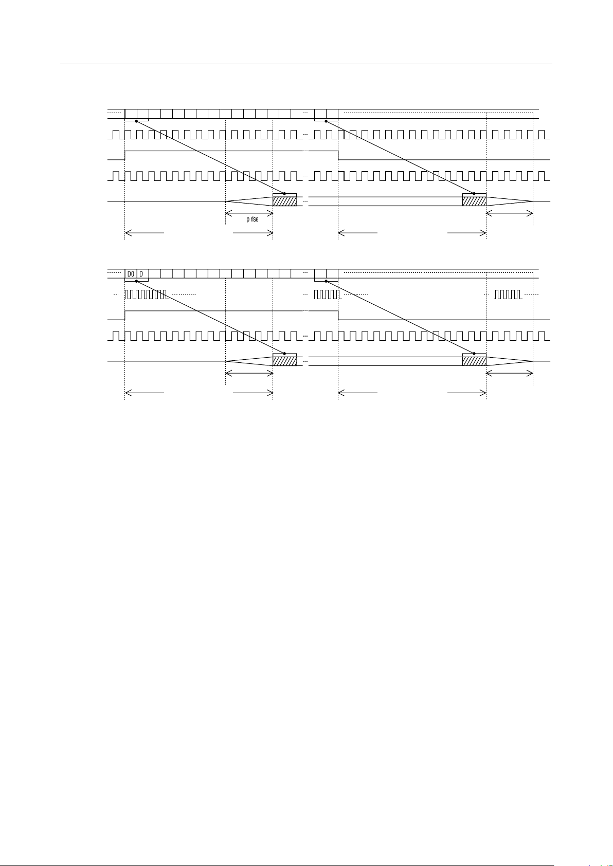
Transmit Clock (TXCO) Timing (When CRM0 - B6 = 1)
TXCI
(3.84 MHz)
TXCO
(384 kHz)
1234
t
XDM1
5678910
t
XDM2
Transmit Burst Position (BSTO) Output Timing (When CRM0 - B6 = 0)
TXCI
(384 kHz)
TXW
BSTO
12 9
10 N
t
XDM3
N+1
Figure 9 Modem Unit Transmit Side (Modulator Side) Digital I/O Timing
N+1
t
SXM
t
XDM1
N+16 N+17 N+18
t
XDM4
Receive Side Data I/O Timing
SLS
RXC
t
RDM1
RXD
Figure 10 Modem Unit Receive Side (Demodulator Side) Digital I/O Timing
Serial Port Timing for Microcontroller Interface
DENM
t
t
M7
M5
t
M8
EXCKM
DINM
DOUTM
t
M1
t
M2
123456
t
M3
t
M4
t
M6
W/R A2 A1 A0 B7
B7
11 12
t
M9
B1 B0
B1 B0
t
RDM2
t
M12
t
M10
t
M11
Figure 11 Modem Unit Serial Control Port Interface
26/42
Page 27

¡ Semiconductor MSM7586-01/03
(CODEC Unit)
Transmit Side PCM, ADPCM Timing
BCLK
XSYNC
PCMSO
BCLK
t
t
0
XSC
XSC
12345678910
t
SXC
t
XDC1
t
WSC
t
XDC2
MSB LSB
t
SDXC
123456789100
t
SXC
XSYNC
IS
t
SDXC
t
XDC1
t
XDC2
MSB LSB
Receive Side PCM, ADPCM Timing
BCLK
RSYNC
IR
t
RSC
12345678910
t
SRC
t
DSC
t
DHC
t
WSC
MSB
t
XDC3
LSB
t
XDC3
t
XDC3
BCLK
t
RSC
t
SRC
123456789100
RSYNC
t
RDC2
MSB LSB
PCMRO
t
SDXC
t
RDC1
Figure 12 CODEC Unit PCM, ADPCM Interface
Serial Port Timing for Microcontroller Interface
DENC
t
C5
t
C7
t
C8
EXCKC
DINC
t
C2
123456
t
C1
t
C3
t
C4
t
C6
W/RA2A1A0B7
t
11 12
t
C9
B1 B0
RDC3
t
C12
t
t
C10
C11
DOUTC
B7
B1 B0
Figure 13 CODEC Unit Serial Control Port Interface
27/42
Page 28

¡ Semiconductor MSM7586-01/03
g
Modem Unit Mode State Transition Time
Mode
A*
PDN1 = 1
Values not indicated are
Note:
less than 1 ms.
1 ms
Mode
B
Mode
C
Standby mode (PDN0 = 0)
Communication mode (PDN0 = 1)
40 ms
Mode
E
PDN1 = 1
PDN2 = 0
Figure 14 Modem Unit Power Down State Transition Time
5 ms
Mode
Mode
PDN1 = 0
PDN2 = 0
D
PDN1 = 0
PDN2 = 0
G
PDN1 = 1
PDN2 = 1
5 ms
40 ms5 ms
Mode
PDN1 = 0
PDN2 = 1
F
PDN1 = 0
PDN2 = 1
*Note that this state
clears the re
ister.
28/42
Page 29

¡ Semiconductor MSM7586-01/03
Modem Unit Demodulator Control Timing Diagram (Example)
Demodulator unit
Modulator input data
GR1
1st slot
PDN2
SLS
"0"
AFC
RXD
R1
RXC
(1) Control ch/
synchronous burst
(SS + PR = 64 bits)
G G G G G G G G R R R R SS SS PR PR PR UW CR CR G G G G G G GG
RXD
240 bits
625 ms
AFC*
RPR
RCW*
(2) When synchronization is not yet established
AFC*
RPR
RCW*
G
64 bits
56 bits
(3) Communication ch
(SS + PR = 8 bits)
G G G G G G G G R R R R SS SS PR PR PR UW CR CR G G G G G G GG
RXD
AFC
RPR
RCW
Figure 15 Modem Unit Demodulator Timing Diagram Example
8 bits
"0"
Less than 30 bits
*AFC and RCW may be controlled at the same timing.
G: Guard bit
R: Ramp bit
SS: Start symbol bit
PR: Preamble bit
UW: Unique word bit
CR: CRC bit
29/42
Page 30

¡ Semiconductor MSM7586-01/03
FUNCTIONAL DESCRIPTION
Control Register Description Table
(Modem Unit)
(1) CRM0 (Basic Operation Mode Setting)
B0B1B2B3B4B5B6B7
CRM0
Initial Value (Note)
—
0
TXC
SEL
0
Note: The initial value is the value set when a reset is applied by the RESET pin.
B7, B2: ..... Not used
B6: ............ Transmission timing clock selection
0: TXCI input: 384 kHz TXCO output: APLL 384 kHz output
Transmission data TXD is input synchronized to the rise of TXCI. APLL is
ON.
1: TXCI input: 3.84 MHz TXCO output: 384 kHz (TXCI divided by 10)
Transmission data TXD is input synchronized to the rise of TXCO. APLL
is OFF.
B5: Modulation OFF/ON control
0: Modulation ON 1: Modulation OFF
B4, B3: ..... Receive side input IF frequency selection
(0,0), (0,1): 1.2 MHz
(1,0): 10.8 MHz
(1,1): 10.7 MHz/10.75 MHz
B1, B0: ..... Device test control bit
Since it is used for LSI testing, it is normally set to "0."
MOD
OFF
0
IFSEL1
0
IFSEL0
0
—
TEST1
0
0
TEST0
0
30/42
Page 31

¡ Semiconductor MSM7586-01/03
(2) CRM1 (I and Q Gain Adjustment)
B0B1B2B3B4B5B6B7
CRM1
Initial Value
Ich
GAIN3
0
Ich
GAIN2
Ich
GAIN1
Ich
GAIN0
Qch
GAIN3
Qch
GAIN2
Qch
GAIN1
Qch
GAIN0
0000000
B7 to B4: ....I+ and I- output gain setting: 3 mV steps (refer to Table 4)
B3 to B0: ....Q+ and Q- output gain setting: 3 mV steps (refer to Table 4)
Table 4: I and Q Gain Setting Table
CRM1 - B7 B6 B5 B4
CRM1 - B3 B2 B1 B0
0 111
0 110
0 101
0 100
0 011
0 010
0 001
0 000
1 111
1 110
1 101
1 100
1 011
1 010
1 001
1 000
Description
Amplitude value: 1.042 reference value
1.036
1.030
1.024
1.018
1.012
1.006
1.000 (Reference value)
0.994
0.988
0.982
0.976
0.970
0.964
0.958
0.952
(3) CRM2 (Output to R7 to R4 pins)
CRM2
Initial Value
B7
R7
0
B6
R6
0
B7 to B4: ....Output to R7 to R4 pin
B5
R5
0
B4
R4
0
B3
—
0
B2
—
0
B1
—
0
B0
—
0
31/42
Page 32

¡ Semiconductor MSM7586-01/03
(4) CRM3 (I- Output Offset Voltage Adjustment)
B0B1B2B3B4B5B6B7
CRM3
Initial Value
Ich
Offset4
0
Ich
Offset3
Ich
Offset2
Ich
Offset1
Ich
Offset0
—
—
00000
0
—
0
B7 to B3: ....I- output pin offset voltage adjustment (refer to Table 5)
B2 to B0: ....Not used
(5) CRM4 (Q- Output Offset Voltage Adjustment)
B0B1B2B3B4B5B6B7
CRM4
Initial Value
Qch
Offset4
0
Qch
Offset3
Qch
Offset2
Qch
Offset1
Qch
Offset0
—
—
00000
0
—
0
B7 to B3: ....Q- output pin offset voltage adjustment (refer to Table 5)
B2 to B0: ....Not used
Table 5: Ich and Qch Offset Adjustment Values
CRM3 - B7 B6 B5 B4 B3
CRM4 - B7 B6 B5 B4 B3 CRM4 - B7 B6 B5 B4 B3
0 1111
0 1110
0 1101
0 1100
0 1011
0 1010
0 1001
0 1000
0 0111
0 0110
0 0101
0 0100
0 0011
0 0010
0 0001
0 0000
Offset Voltage
+45 mV
+42 mV
+39 mV
+36 mV
+33 mV
+30 mV
+27 mV
+24 mV
+21 mV
+18 mV
+15 mV
+12 mV
+9 mV
+6 mV
+3 mV
0 mV
CRM3 - B7 B6 B5 B4 B3
1
1
1
1
1
1
1
1
1
1
1
1
1
1
1
1
1111
1110
1101
1100
1011
1010
1001
1000
0111
0110
0101
0100
0011
0010
0001
0000
Offset Voltage
–3 mV
–6 mV
–9 mV
–12 mV
–15 mV
–18 mV
–21 mV
–24 mV
–27 mV
–30 mV
–33 mV
–36 mV
–39 mV
–42 mV
–45 mV
–48 mV
32/42
Page 33

¡ Semiconductor MSM7586-01/03
(6) CRM5 (IC Test)
B0B1B2B3B4B5B6B7
CRM5
Initial Value
ICT5
0
ICT4 ICT3 ICT2
LOCAL
INV1
LOCAL
INV0
ICT1 ICT0
0000000
B7 to B4: ....LSI test control bit
Note: Since B7 to B4 of CRM5 are used for LSI testing, they should normally be set to "0".
B3, B2: ....... Local inverted mode setting bit
(Use if the phase of the demodulator side IF input is inverted due to the
system configuration.)
(0,0): Normal mode(1,1): Local inverted mode
B1: ..............Waveform shaping mode switching bit of the oscillator circuit unit clock
(When using a master clock external input, increase the X1 pin input
sensitivity.)
0: Normal mode 1: Clock waveform shaping mode
B0: ..............Oscillator circuit unit power on control bit
0: Normal mode 1: Oscillator circuit unit is always powered on
33/42
Page 34

¡ Semiconductor MSM7586-01/03
(CODEC Unit)
(1) CRC0 (Basic Operation Mode Settings)
B0B1B2B3B4B5B6B7
CRC0
Initial Value
A/m
SEL
—
PDN
ALL
000
——
—
—
000
0
PDN
SAO/AOUT
0
B7: ........................... PCM interface companding selection 0: m-law 1: A-law
B6, B4, B3, B2, B1: . Not used (These pins are used to test the device. They should be set
to "0" during normal operation.)
B5: ........................... Power down (entire unit) 0: Power ON 1: Power down
ORed with the inverse of the external power down signal. When
using this data, set PDN3 to "1."
B0: ........................... The sounder output amp (SAO, GSX3) and receiver system output
amp (VFRO, AOUT+, AOUT-) power down control
0: The output amp of the side not selected by CRC4 - B5 is powered
down.
1: The sounder system output amp and receiver system output
amp are both powered ON.
(2) CRC1 (ADPCM Unit Operation Mode Settings)
CRC1
Initial Value
MODE1
MODE0
TX RESET RX RESET
B7, B6: ....... ADPCM unit compression algorithm selection
(0,0): 32 kbps (0,1): 64 kbps (G.711 through)
(1,0): 24 kbps (1,1): 16 kbps
B5: ..............Transmit side ADPCM reset (according to the G.726
specifications): 1: Reset
The ADPCM reset input width should be 125 ms or more.
B4: ..............Receive side ADPCM reset (according to the G.726
specifications): 1: Reset
The ADPCM reset input width should be 125 ms or more.
B3: ..............Transmit side ADPCM data mute: 1: Mute
B2: ..............Receive side ADPCM data mute: 1: Mute
B1: ..............Not used
B0: ..............Receive side PAD 0: No PAD
1: A PAD with a 12 dB loss is inserted in the receive side voice path
TX MUTE
RX MUTE
000000
—
B0B1B2B3B4B5B6B7
RX PAD
0
0
34/42
Page 35

¡ Semiconductor MSM7586-01/03
(3) CRC2 (PCM CODEC Unit Operation Mode Settings and Transmit/Receive Gain Adjustment)
B0B1B2B3B4B5B6B7
CRC2
Initial Value
TX
ON/OFF
TX
GAIN2
TX
GAIN1
TX
GAIN0
RX
ON/OFF
RX
GAIN2
RX
GAIN1
RX
GAIN0
11001100
B7: ..............Transmit side PCM signal ON/OFF 0: ON 1: OFF
When OFF, transmits a PCM idle pattern.
B6, B5, B4: Transmit side signal gain adjustment (refer to Table 6)
B3: ..............Receive side PCM signal ON/OFF 0: ON 1: OFF
When OFF transmits a PCM idle pattern.
B2, B1, B0: .Receive side signal gain adjustment (refer to Table 6)
Table 6: Receive/Transmit Gain Settings
• MSM7586-01
B6 B5 B4 Transmit Side Gain B2 B1 B0 Receive Side Gain
0 0 0 –6 dB 0 0 0 –6 dB
001 –4 dB 001
010 –2 dB 010
0 1 1 0 dB 0 1 1
100 +2 dB 100
101 +4 dB 101
110 +6 dB 110
111 +8 dB 111
–4 dB
–2 dB
0 dB
+2 dB
+4 dB
+6 dB
+8 dB
• MSM7586-03
B6 B5 B4 Transmit Side Gain B2 B1 B0 Receive Side Gain
0 0 0 –6 dB 0 0 0 –12 dB
001 –4 dB 001
010 –2 dB 010
0 1 1 0 dB 0 1 1
100 +2 dB 100
101 +4 dB 101
110 +6 dB 110
111 +8 dB 111
–9 dB
–6 dB
–3 dB
0 dB
+3 dB
+6 dB
+9 dB
The above gain settings table shows the transmit/receive voice signal gain settings and the
transmit side gain settings for DTMF tones and other tones. Tone signal transmission is enabled
by CRC4 - B6 (discussed later), and the gain setting is set to the levels shown below.
DTMF tones (low group): ................................. –16 dBm0
DTMF tones (high group) and other tones: ... –14 dBm0
For example, if the transmit gain set value is set to +8 dB (B6, B5, B4) = (1, 1, 1), then the following
tones appear at the PCMSO pin.
DTMF tones (low group): ................................. –8 dBm0
DTMF tones (high group) and other tones: ... –6 dBm0
35/42
Page 36

¡ Semiconductor MSM7586-01/03
However, the gain of the receive side tone and the gain of the side tones (path from transmit side
to receive side) are set by the CRC3 register.
(4) CRC3 (Side Tone and Tone Generator Gain Adjustment)
CRC3
Initial Value
B7, B6, B5: ........ Side tone gain adjustment (refer to Table 7)
B4: ..................... Tone generator ON/OFF 0: OFF 1: ON
B3, B2, B1, B0: . Tone generator Receive side gain adjustment (refer to Table 8)
• MSM7586-01
B7
Side Tone
GAIN2
B6
Side Tone
GAIN1
B5
Side Tone
GAIN0
B4
TONE
ON/OFF
B3
TONE
GAIN3
Table 7: Side Tone Gain Settings
B7 B6 B5 Side Tone Gain
000 OFF
0 0 1 –21 dB
0 1 0 –19 dB
0 1 1 –17 dB
1 0 0 –15 dB
1 0 1 –13 dB
1 1 0 –11 dB
1 1 1 – 9 dB
B2
TONE
GAIN2
B1
TONE
GAIN1
0000000
B0
TONE
GAIN0
0
• MSM7586-03
B7 B6 B5 Side Tone Gain
000 OFF
001
010
011
100
101
110
111
–15 dB
–13 dB
–11 dB
– 9 dB
– 7 dB
– 5 dB
– 3 dB
36/42
Page 37

¡ Semiconductor MSM7586-01/03
Table 8: Receive Side Tone Generator Gain Settings
• MSM7586-01
B3 B2 B1 Tone Generator Gain Tone Generator Gain
0 0 0 –36 dB –20 dB
0 0 0 –34 dB
0 0 1 –32 dB
0 0 1 –30 dB
010
010
011
111
B0
0
1
0
1
0
1
0
1
–28
–26
–24
–22
dB
dB
dB
dB
B3 B2 B1
100
100
101
101
110
110
111
111
B0
0
1
0
1
0
1
0
1
–18 dB
–16 dB
–14
dB
–12
dB
–10
dB
– 8
dB
– 6
dB
• MSM7586-03
B3 B2 B1 Tone Generator Gain Tone Generator Gain
0 0 0 –20 dB
0 0 0 –34 dB
0 0 1 –32 dB
0 0 1 –30 dB
010
010
011
111
B0
0
1
0
1
0
1
0
1
OFF
–28
–26
–24
–22
dB
dB
dB
dB
B3 B2 B1
100
100
101
101
110
110
111
111
B0
0
1
0
1
0
1
0
1
–18 dB
–16 dB
–14
dB
–12
dB
–10
dB
– 8
dB
– 6
dB
The receive side tone generator gain settings shown in Table 8 are set with the following levels
as a reference.
DTMF tones (low group): ................................. –2 dBm0
DTMF tones (high group) and other tones: ... 0 dBm0
For example, if the tone generator gain set value is set to -6 dB (B3, B2, B1, B0)=(1, 1, 1, 1), then
tones at the following levels appear at the SAO or VFRO pin.
DTMF tones (low group): ................................. –8 dBm0
DTMF tones (high group) and other tones: ... –6 dBm0
37/42
Page 38

¡ Semiconductor MSM7586-01/03
(5) CRC4 (Tone Generator Operation Mode and Frequency Settings)
B0B1B2B3B4B5B6B7
CRC4
Initial Value
DTMF/OT
HERS SEL
0
TONE
SEND
SAO/
VFRO
TONE4 TONE3
TONE2
00000
TONE1
0
TONE0
0
B7: ........................... Selection of DTMF signal and other tones
(S tone, F tone, R tone, etc.) 0: Other tones 1: DTMF tones
B6: ........................... Transmission side tone transmit
0: Voice signal transmit 1: Tone transmit
B5: ........................... Receive side tone output pin selection
0: VFRO output 1: SAO output
B4, B3, B2, B1, B0: . Tone frequency setting (refer to Table 9)
Table 9: Tone Generator Frequency Settings
(a) When B7 = 1 (DTMF Tones)
B4 B3 B2 B1 B0 Description
* 0 0 0 0 697 Hz + 1209 Hz
* 0 0 0 1 697 Hz + 1336 Hz
* 0 0 1 0 697 Hz + 1477 Hz
* 0 0 1 1 697 Hz + 1633 Hz
* 0 1 0 0 770 Hz + 1209 Hz
* 0 1 0 1 770 Hz + 1336 Hz
* 0 1 1 0 770 Hz + 1477 Hz
* 0 1 1 1 770 Hz + 1633 Hz
(b) When B7 = 0 (Outside of DTMF Tones)
B4 B3 B2 B1 B0 Description
00000
00001
00010
00011 —
00100 —
00101 —
00110 —
00111 —
01000 —
0 1 0 0 1 400 Hz Single tone
01010 —
01011 —
01100 —
01101 —
01110 —
0 1 1 1 1 1000 Hz Single tone
2730 Hz/2500 Hz 8 Hz Wamble
2000 Hz/2667 Hz 8 Hz Wamble
1000 Hz/1333 Hz 8 Hz Wamble
B4 B3 B2 B1 B0 Description
*1000 852 Hz + 1209 Hz
*1001 852 Hz + 1336 Hz
*1010 852 Hz + 1477 Hz
*1011 852 Hz + 1633 Hz
*1100 941 Hz + 1209 Hz
*1101 941 Hz + 1336 Hz
*1110 941 Hz + 1477 Hz
*1111 941 Hz + 1633 Hz
B4 B3 B2 B1 B0 Description
10000 —
1
0001 1300 Hz Single tone
1
0010 1333 Hz Single tone
1
0011 —
1
0100 —
1
0101 2000 Hz Single tone
1
0110 —
1
0111 —
1
1000 —
1
1001 —
1
1010 —
1
1011 —
1
1100 2667 Hz Single tone
1
1101 —
1
1110 2730 Hz Single tone
1
1111 —
38/42
Page 39

¡ Semiconductor MSM7586-01/03
(6) CRC5 (Control of Switches, etc.)
B0B1B2B3B4B5B6B7
CRC5
Initial Value
SW1
CONT
0
SW2
CONT
SW3
CONT
SW4/5
CONT
—
TOUT3
CONT
00000
TOUT2
CONT
TOUT1
CONT
00
B7, B6: ....... SW1, SW2 control 0: Open 1: Closed
B5: ..............SW3 control 0: Open 1: Closed
B4: ..............SW4/5 control 0: SW4 open, SW5 closed
1: SW4 closed, SW5 open
B2, B1, B0: .TOUT3 to 1 control 0: TOUT3 to 1 disable
1: TOUT3 to 1 enable
(7) CRC6 (VOX Function Control)
B0B1B2B3B4B5B6B7
CRC6
Initial Value
VOX
ON/OFF
0
ON
LVL1
ON
LVL0
OFF
TIME
VOX
IN
RX NOISE
LEVEL SEL
00000
RX NOISE
LVL1
RX NOISE
LVL0
00
B7: ..............VOX function ON/OFF 0: OFF 1: ON
B6, B5: ....... Transmit side voice/silence detector level settings (For the signal of 1kHz)
MSM7586-01
(0,0): –30 dBm0 (0,1): –35 dBm0
(1,0): –40 dBm0 (1,1): –45 dBm0
MSM7586-03
(0,0): –20 dBm0 (0,1): –26 dBm0
(1,0): –32 dBm0 (1,1): –38 dBm0
B4: .............. Hangover time (refer to Fig. 7) settings 0: 160 ms 1: 320 ms
B3: ..............Receive side VOX input signal
0: Internal background noise transmit 1: Voice receive signal transmit
When using this data, set the VOXI pin to "0."
B2: ..............Receive side background noise level setting
0: Internal automatic setting 1: External (by B1, B0) setting
Internal automatic setting Æ Sets to the voice signal level when B3 (VOXI)
changes from "1" to "0."
B1, B0: ....... External setting background noise level
(0,0): No noise (0,1): –55 dBm0
(1,0): –45 dBm0 (1,1): –35 dBm0
39/42
Page 40

¡ Semiconductor MSM7586-01/03
(8) CRC7 (Detect Register: Read-only)
B0B1B2B3B4B5B6B7
CRC7
Initial Value
VOX
OUT
0
Silent Level1Silent Level
0
———
—
—
***00
**
B7:........................... Transmit side voice/silence detection 0: Silence 1: Voice
B6, B5: .................... Transmit side silence level (indicator)
MSM7586-01
(0,0):Below –60 dBm0 (0,1): –50 to –60 dBm0
(1,0): –40 to –50 dBm0 (1,1): Above –40 dBm0
MSM7586-03
(0,0):Below –50 dBm0 (0,1): –40 to –50 dBm0
(1,0): –30 to –40 dBm0 (1,1): Above –30 dBm0
Note: These outputs are enabled when the VOX function is turned ON by CRC6 - B7.
B4, B3, B2, B1, B0: . Not used
40/42
Page 41

¡ Semiconductor MSM7586-01/03
APPLICATION CIRCUIT
MSM7586
RF
MIC
Speaker
Sounder
Ringer
100
VDDM
1
VDAM
30
VDDC
29
VDAC
7
SGM
10
SGCR
11
SGCT
+
1 mF
1 mF
R7
R4
R5
10 mF
–
9
AGC
67
DGC
8
AGM
68
DGM
97
IFIN
2
Q–
3
Q+
4
I–
5
I+
12
AIN1+
13
AIN1–
14
GSX1
18
AIN2
19
GSX2
25
AOUT+
24
AOUT–
23
PWI
22
VFRO
26
SAO
27
AIN3
28
GSX3
32
AIN4
33
GSX4
38
TOUT1
39
TOUT2
40
TOUT3
90
MCK
91
IFCK
95
X1
92
X2
R2
+
1 mF
10 mF
–
1000 pF
SGCT
R3
R6
R8
+
1 mF
–
10 mF
1 mF
R11 mF
19.2 MHz
DOUTM
PCMSO
PCMRO
PDN2
PDN1
PDN0
DENM
EXCKM
DINM
BSTO
TXCI
TXCO
TXD
TXW
RXD
RXC
RPR
AFC
RCW
SLS
RXSC
PDN3
RESET
DINC
DOUTC
EXCKC
DENC
BCLK
XSYNC
RSYNC
PCMSI
PCMRI
VOXI
VOXO
87
88
89
79
78
77
76
69
71
72
73
74
81
82
83
84
85
98
99
41
42
44
45
46
47
61
60
59
VDDC
57
56
55
IS
53
IR
52
51
49
50
500 W
MODEM
CONT.
ADPCM
CODEC
CONT.
R1 ≥ Output drive resistance of MIC
R2//R3 ≥ 20 kW
R4, R5, R7 ≥ 20 kW
R6//Input resistance of speaker ≥ 1.2 kW
R8//Input resistance of sounder ≥ 150 W
41/42
Page 42

¡ Semiconductor MSM7586-01/03
PACKAGE DIMENSIONS
(Unit : mm)
TQFP100-P-1414-0.50-K
Mirror finish
Package material
Lead frame material
Pin treatment
Solder plate thickness
Package weight (g)
Epoxy resin
42 alloy
Solder plating
5 mm or more
0.55 TYP.
Notes for Mounting the Surface Mount Type Package
The SOP, QFP, TSOP, SOJ, QFJ (PLCC), SHP and BGA are surface mount type packages, which
are very susceptible to heat in reflow mounting and humidity absorbed in storage.
Therefore, before you perform reflow mounting, contact Oki’s responsible sales person for the
product name, package name, pin number, package code and desired mounting conditions
(reflow method, temperature and times).
42/42
 Loading...