

Page 1

E2U0035-16-X2
¡ Semiconductor MSM7582/7582B
¡ Semiconductor
This version: Jan. 1998
Previous version: Nov. 1996
MSM7582/7582B
p/4 Shift QPSK MODEM
GENERAL DESCRIPTION
The MSM7582/7582B are CMOS ICs for the p/4 shift QPSK modem developed for the digital
cordless telephone systems.
The devices are designed for Personal and Cell station applications, the MSM7582B is the
improved MSM7582 in modulator burst rise-up and fall-down characteristics.
FEATURES
••
• Single Power Supply (VDD: 2.7 V to ␣ 3.6 V)
••
(Modulator Block)
••
• Built-in Root Nyquist Filter for Baseband Limiting (50% Roll-off)
••
••
• Ramp Bit for Burst Signal Rise-up:
••
MSM7582/1.75 symbols
MSM7582B/2.0 symbols
••
• Ramp Bit for Burst Signal Fall-down:
••
MSM7582/2.75 symbols
MSM7582B/2.0 symbols
••
• Built-in D/A converters for Analog Output of Quadrature Signal I/Q Components and Power
••
Envelope Output
••
• Differential I/Q Analog output format
••
••
• I/Q Output DC Offset / Gain Adjustable
••
I2 + Q
2
(Demodulator Block)
••
• Full Digital System, p/4 shift QPSK Demodulation
••
••
• Input IF signal Frequency Selectable: 1.2/10.7/10.75/10.8 MHz
••
••
• Built-in Clock Recovery: 4 Circuits useful for Cell station
••
(Common)
••
• Various Power-down Modes: Tramsmit/Receive Independant
••
••
• Built-in Precise Analog Voltage Reference
••
••
• MCU Serial Interface for Mode setting and Built-in Test circuit
••
••
• Test Modes: Eye pattern / AFC Compensating Signal / Phase Detection Signal, possible to
••
monitor
••
• Transmission Speed: 384 kbps
••
••
• Low Power consumption
••
Operating mode : 15 mA Typ. / Modulator (VDD = 3.0 V)
: 9 mA Typ. / Demodulator (VDD = 3.0 V)
Whole system Power-down mode: 0.01 mA Typ. (VDD = 3.0 V)
••
• Package:
••
32-pin plastic TSOP (TSOPI32-P-814-0.50-1K)(Product name : MSM7582TS-K)
(Product name : MSM7582BTS-K)
1/24
Page 2
¡ Semiconductor MSM7582/7582B
2/24
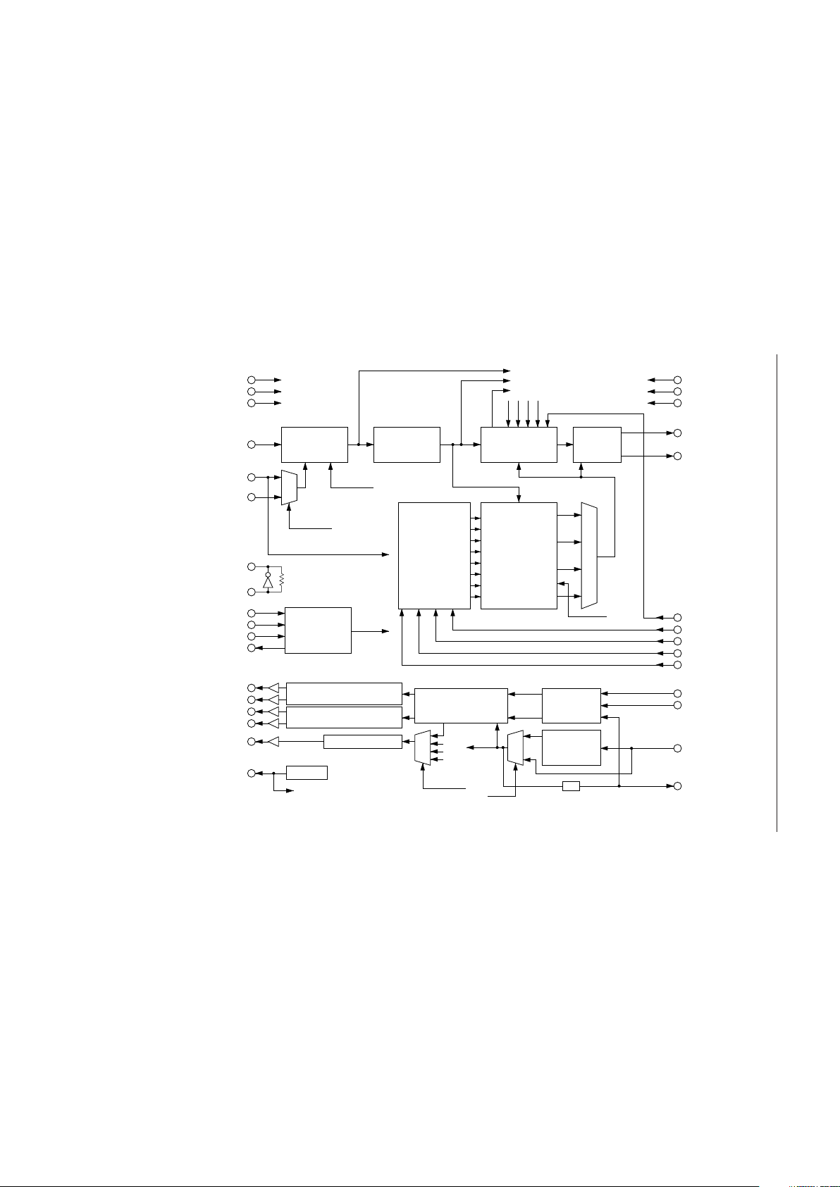
BLOCK DIAGRAM
IFIN
AGND
DGND
V
DD
Phase Detector Delay Detector
IFCK
MCK
X1
DEN
EXCK
DIN
DOUT
S
E
L
X2
Control
Register (CR)
To each
block
PDN0
PDN1
PDN2
AFC
DPLL
Decision
Unit
RXC
RXD
S
E
L
SLS1
SLS2
+
1
-
1
+
1
-
1
+
1
I+
I–
Q+
Q–
ENV
Root Nyquist
LPF
S
E
L
S/P
MAPPING
S
E
L
APLL
TXD
TXW
TXCI
1/10
TXCO
SG
To internal SG
To each block
IFSEL0
(From CR)
IFSEL1
(From CR)
SL4
SL3
SL2
SL1
To monitor output
of each block
To modem ENV
PS/CS
RPR
RCW
AFC
TEST1, TEST0
(From CR)
To
Monitor
output of
each block
TXCSEL
(From CR)
3.84 MHz
384 kHz
Decoder
ENV D/A CONV
VREF
I ± D/A CONV
Q ± D/A CONV
To D/A
Page 3

¡ Semiconductor MSM7582/7582B
PIN CONFIGURATION (TOP VIEW)
AGND
SG
I+
I–
Q+
Q–
ENV
PDN0
PDN1
PDN2
V
DD
SLS1
SLS2
RCW
AFC
RPR
10
11
12
13
14
15
16
1
2
3
4
5
6
7
8
9
32-Pin Plastic TSOP
32
31
30
29
28
27
26
25
24
23
22
21
20
19
18
17
DGND
IFIN
TXCI
TXCO
TXD
TXW
DEN
EXCK
DIN
DOUT
MCK
RXD
RXC
IFCK
X2
X1
3/24
Page 4
¡ Semiconductor MSM7582/7582B
PIN AND FUNCTIONAL DESCRIPTIONS
TXD
Transmit data input for 384 kbps.
TXCI
Transmit clock input.
When the control register CR0 – B6 is “0”, a 384 kHz clock pulse synchronous with TXD should
be input to this pin. This clock pulse should be continuous because these devices use APLL to
generate the internal clock pulse.
When CR0 – B6 is “1”, a 3.84 MHz clock pulse should be input to this pin. When the 3.84 MHz
clock pulse is applied, TXCO outputs a 384 kHz clock pulse, which is generated by dividing the
3.84 MHz to TXCI by 10. The transmit data, synchronous 384 kHz clock pulse, should be input
to the TXD. In this case the devices do not use APLL, and the 3.84 MHz clock pulse need not be
continuous. (Refer to Fig. 1.)
TXCO
Transmit clock output.
When CR0 - B6 is “0”, TXCO outputs the 384 kHz clock pulse (APLL output) for monitoring
purposes. When CR0 – B6 is “1”, this pin outputs a 384 kHz clock pulse generated by dividing
the TXCI input by 10. (Refer to Fig. 1.)
When CR0 – B6 = “0” and CR5 – B7 = “1”, this pin outputs the burst timing position.
TXW
Transmit data window input.
The transmit timing signal for the burst data is input to the device pin. If TXW is “1”, the
modulation data is output. However, the MSM7582 is different from the MSM7582B in the ramp
response time for burst rise-up and burst fall-down of I, Q modulated outputs, as shown in the
table below. (Refer to Fig, 1-1 for the MSM7582 and Fig, 1-2 for the MSM7582B)
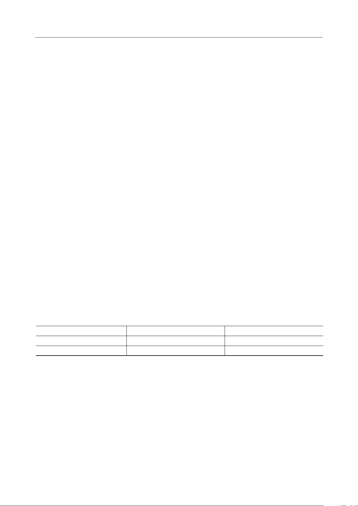
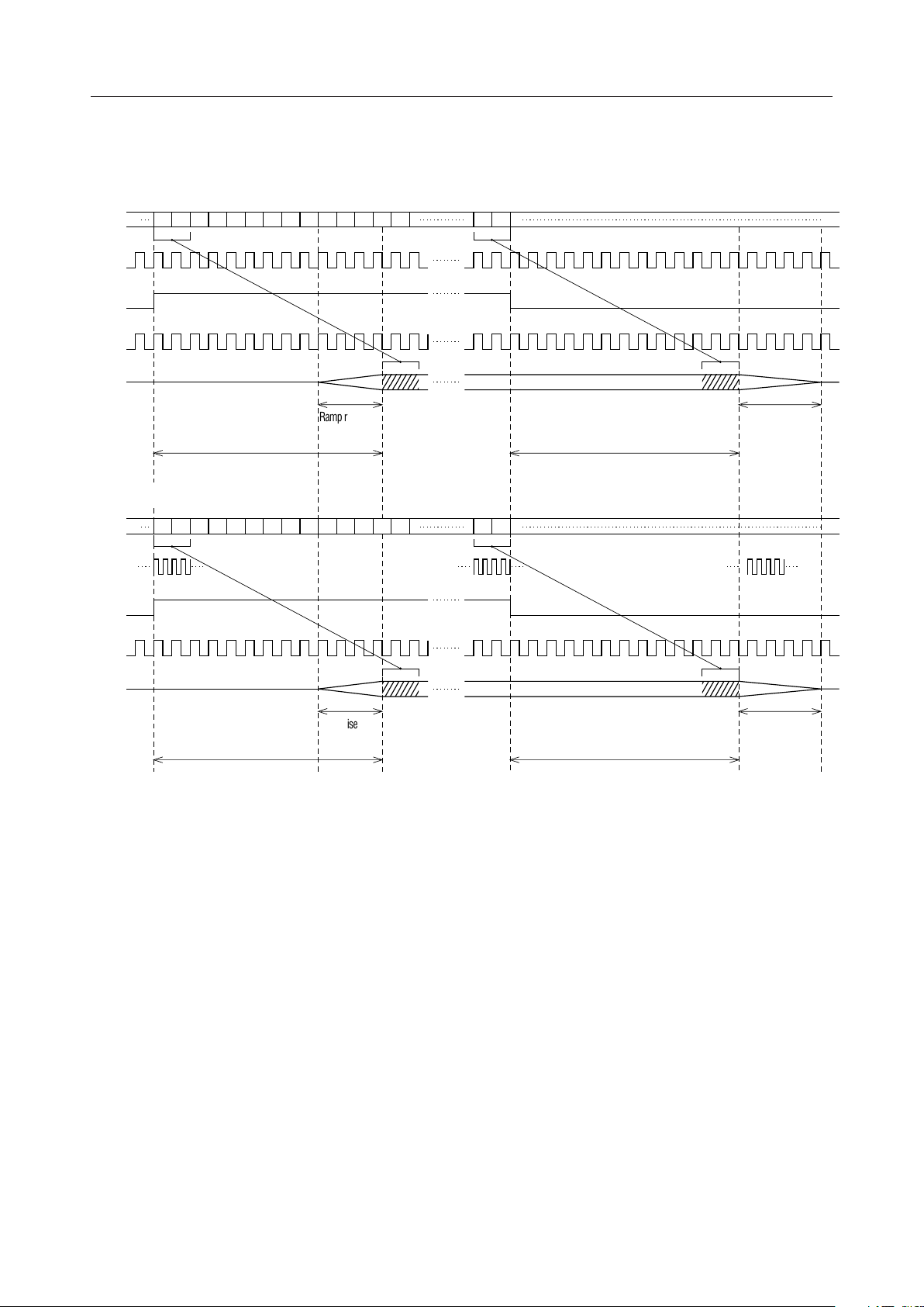
MSM7582 MSM7582B
Ramp Rise-up 1.75 symbols 2 symbols
Ramp Fall-down 2.75 symbols 2 symbols
The TXCO burst position output timing discribed before, is different, according to this table.
4/24
Page 5
¡ Semiconductor MSM7582/7582B
,
MSM7582
(1) CR0 – B6 = "0"
D0 D1 D2 D3 D4 D5 D6 D7 D8 D9
TXD
TXCI
(384 kHz)
TXW
TXCO
(384 kHz)
I, Q
Delay of 6.25 symbols
(2) CR0 – B6 = "1"
D0 D1 D2 D3 D4 D5 D6 D7 D8 D9
TXD
TXCI
(3.84 MHz)
TXW
TXCO
(384 kHz)
I, Q
D10 D11 D12 D13
Ramp rise-up
1.75 symbols
D10 D11 D12 D13
Dn-1
Dn-1
Dn
Ramp
Delay of 6.25 symbols
Dn
Fall-down
2.75 symbols
Delay of 6.25 symbols
Ramp rise-up
1.75 symbols
Delay of 6.25 symbols
Figure 1-1 Transmit Timing Diagram
Ramp
Fall-down
2.75 symbols
5/24
Page 6
¡ Semiconductor MSM7582/7582B
,
MSM7582B
(1) CR0 – B6 = "0"
D0 D1 D2 D3 D4 D5 D6 D7 D8 D9
TXD
TXCI
(384 kHz)
TXW
TXCO
(384 kHz)
I, Q
Delay of 6.25 symbols
(2) CR0 – B6 = "1"
D0 D1 D2 D3 D4 D5 D6 D7 D8 D9
TXD
TXCI
(3.84 MHz)
TXW
TXCO
(384 kHz)
I, Q
D10 D11 D12 D13
Ramp rise-up
2 symbols
D10 D11 D12 D13
Dn-1
Dn-1
Dn
Ramp fall-down
Delay of 6.25 symbols
Dn
2 symbols
Delay of 6.25 symbols
Ramp rise-up
2 symbols
Delay of 6.25 symbols
Ramp fall-down
2 symbols
Figure 1-2 Transmit Timing Diagram
I+, I–
Quadrature modulation signal I component differential analog outputs.
Their output levels are 500 mVpp with 1.6 Vdc as the center value. The output pin load conditions
are: R ≥ 10 kW, C ≤ 20 pF. The gain of these pins can be adjusted using the control register CR1
– B7 to B4, and the offset voltage at the I– pin can be adjusted using CR3 – B7 to B3.
Q+, Q–
Quadrature modulation signal Q component differential analog outputs.
Their output levels are 500 mVPP with 1.6 Vdc as the center value. The output pin load conditions
are: R ≥ 10 kW, C ≤ 20 pF. The gain of these pins can be adjusted using the control register CR1
– B3 to B0, and the offset voltage at the Q– pin can be adjusted by using CR4 – B7 to B3.
6/24
Page 7
¡ Semiconductor MSM7582/7582B
ENV
Quadrature modulation signal envelope (
I2 + Q
2
)output.
Its output level is 500 mVPP with 1.6 Vdc as a center value. The output pin load conditions are
: R ≥ 10 kW, C ≤ 20 pF. The gain of this output can be adjusted using the control register CR2 – B7
to B4.
This pin is also used to monitor eye pattern, AFC Compensating signal, and phase defection of
the demodulator block during the test mode. Refer to the description of the control register for
details.
SG
Internal reference voltage output.
The output voltage is about 2.0 V. A bypass capacitor should be connected between this pin and
the AGND pin.
PDN0, PDN1, PDN2
Inputs for power-down control.
PDN0 controls the standby / communication modes, PDN1 controls the modulator, and PDN2
controls the demodulator. Refer to Table 1 for details.
Table-1 Power Down Control
PDN0
Standby
Mode
Communication
Mode
PDN2 PDN1
0 0/1 1
000
010
100
101
110
111
Function
All power-down. The control register is reset.
All power-down. The control register is not reset.
Modulator power is off (VREF and PLL power are also off).
Demodulator power is on.
Modulator power is off (VREF and PLL power is on).
I and Q outputs are in a high-impedance state.
Only demodulator clock recovery block power is on.
Modulator power is on
Only demodulator clock recovery block power is on.
Modulator power is off (VREF and PLL power is on).
I and Q outputs are in a high-impedance state.
Demodulator power is on.
Modulator power is on
Demodulator power is on.
Mode
Mode A
Mode B
Mode C
Mode D
Mode E
Mode F
Mode G
V
DD
+3 V power supply voltage.
AGND
Analog signal ground.
DGND
Digital signal ground.
AGND and DGND are not connected in the device. This pin should be tied to the AGND pin on
the PCB as close as possible from the device.
7/24
Page 8
¡ Semiconductor MSM7582/7582B
MCK
Master clock input.
The clock frequency is 19.2 MHz.
IFIN
Modulated signal input for the demodulator block.
Select the IF frequency from 1.2 MHz, 10.7 MHz, 10.75 MHz, and 10.8 MHz, based on CR0 – B4
and B3.
IFCK
Clock signal input for demodulator block IF frequencies (10.7 MHz or 10.75 MHz).
If the IF frequency is 10.7 MHz, 19.0222 MHz should be supplied. When it is 10.75 MHz, 19.1111
MHz should be supplied. When the IF frequency is 1.2 MHz or 10.8 MHz, set this pin to “0” or
“1”. (Refer to Fig. 2.)
X1, X2
Crystal oscillator connection pins.
When supplying a 19.0222 MHz or 19.1111 MHz clock to IFCK, use these pins (Refer to Fig. 2.)
When IFIN = 10.7 MHz or 10.75 MHz
MSM7582/7582B
X1 IFCK
19.0222 MHz or 19.1111 MHz
X2
When IFIN = 1.2 MHz or 10.8 MHz
MSM7582/7582B
X1 IFCK
X2
Figure 2 How to Use IFCK, X1, and X2
RXD, RXC
Receive data and clock output. When power is turned on, the outputs of circuits selected by SLS1
and SLS2 appear at these pins. (Refer to Fig. 3)
RXD1
RXC
SLS2
SLS1
The recovery data and clock pulse are selected
asynchronously using the SLS signals.
Figure 3 RXD and RXC Timing Diagram
8/24
Page 9

¡ Semiconductor MSM7582/7582B
SLS2, SLS1
Receiver slot select signal inputs.
The devices have four sets of clock recovery circuit to each channel and four AFC information
storage registers. One these circuits is selected from a combination of the signals at these pins.
(SLS2, SLS1) = (0, 0): Slot 1, (0, 1): Slot 2
(1, 0): Slot 3, (1, 1): Slot 4
RPR
High-speed phase clock control signal input for the clock recovery circuit.
If this pin is “1”, the clock recovery circuit starts in the high-speed phase clock mode. When the
phase difference is less than a defined value, the circuit shifts to the low-speed phase clock mode
automatically. When this pin is “0”, the circuit is always in the low-speed phase clock mode.
AFC
AFC operation range specification signal input.
As shown in Fig. 4, the AFC information is reset when both AFC and RPR are set to “1”. AFC
operation starts after a fixed number of clock cycles and after the AFC information is reset. If RPR
is set to “1”, an average number of times that AFC turns on is low. If RPR is “0”, AFC is high. If
AFC is “0”, frequency error is not calculated, but the frequency is corrected using an error that
is held.
RCW
Clock recovery circuit operation ON/OFF control signal input. If RCW pin is “0”, DPLL does not
make any phase corrections.
(CASE1)
AFC
RPR
Average number of times
AFC is high.
AFC information
is maintained.
AFC information
is maintained.
(CASE2)
AFC
RPR
AFC information
is reset.
The clock recovery circuit
starts with the previous
AFC information.
Average
number of times
AFC is low.
"0"
Average number of times
AFC is high.
Figure 4 AFC Control Timing Diagram
9/24
Page 10

¡ Semiconductor MSM7582/7582B
,
DEN , EXCK, DIN, DOUT
Serial control ports for the microprocessor interface.
The MSM7582 and MSM7582B contain a 6-byte control register. An external CPU uses these pins
to read data from and write data to the control register. DEN is an enable signal input pin. EXCK
is a data shift clock pulse input pin. DIN is an address and data input pin. DOUT is a data output
pin. Figure 5 shows an input/output timing diagram.
DEN
EXCK
W
A2
DIN
A1 A0 B7 B6 B5 B4 B3 B2 B1 B0
DOUT
DEN
EXCK
DIN
DOUT
High Impedance
(a) Data Write Timing Diagram
R A2A1A0
High Impedance
B7 B6 B5 B4 B3 B2 B1 B0
(b) Data Read Timing Diagram
Figure 5 MCU Interface Input/Output Timing Diagram
10/24
Page 11

¡ Semiconductor MSM7582/7582B
The register map is shown below
Table-2 Control Register Map
Register
CR0
CR1
CR2
CR3
CR4
CR5
Address
A2 A1 A0
000
001
010
011
100
101
B7 B6 B5 B4 B3 B2 B1 B0
PS/CS
Ich
GAIN3
ENV
GAIN3
Ich
Offset4
Qch
Offset4
BSTO
ENBL
TXCSEL
Ich
GAIN2
ENV
GAIN2
Ich
Offset3
Qch
Offset3
ICT6 ICT5 ICT4
MODOFF
Ich
GAIN1
ENV
GAIN1
Ich
Offset2
Qch
Offset2
R/W : Read/Write enable R : Read-only register
Data
IFSEL1 IFSEL0
Ich
GAIN0
ENV
GAIN0
Ich
Offset1
Qch
Offset1
Qch
GAIN3
————
Ich
Offset0
Qch
Offset0
LOCAL
INV1
ENVSEL
Qch
GAIN2
———
———
LOCAL
INV0
TEST1 TEST0
Qch
GAIN1
CLK
SEL1
Qch
GAIN0
CLK
SEL0
R/W
R/W
R/W
R/W
R/W
R/W
R/W
11/24
Page 12

¡ Semiconductor MSM7582/7582B
ABSOLUTE MAXIMUM RATINGS
Parameter
Power Supply Voltage
Digital Input Voltage
Operating Temperature
Storage Temperature
RECOMMENDED OPERATING CONDITIONS
Parameter
Power Supply Voltage V
Symbol
V
DD
V
DIN
T
op
T
STG
Symbol
DD
Condtion
—
—
—
—
= 2.7 V to 3.6 V, Ta = –25°C to +70°C)
(V
DD
Rating
0 to 5
–0.3 to V
–25 to +70
–55 to +150
DD
Unit
+0.3
Condtion Min. Typ. Max. Unit
— 2.7 — 3.6 V
Operating Temperature Range Ta — –25 — +70 °C
Input High Voltage V
Input Low Voltage V
Master Clock Frequency f
f
Modulator Input Frequency
f
f
Demodulator Input Frequency
f
Clock Duty Cycle D
IF Input Duty Cycle D
All digital input pins
IH
All digital input pins
IL
MCK
MCK
TXC1
TXC2
IFCK (when IFIN = 10.7 MHz)
IFCK1
IFCK (when IFIN = 10.75 MHz)
IFCK2
MCK, IFCK, TXCI 40 50 60 %
CCK
IFCK 45 50 55 %
CIF
0.45 ¥ V
0— V
— 19.2 —
50 ppm
50 ppm
—VDDV
DD
19.0222 +
19.1111 +
0.16 ¥ V
50 ppm
50 ppm
DD
V
V
°C
°C
MHz
kHz— 384 —TXCI (when CR0 – B6 = "0")
MHz— 3.84 —TXCI (when CR0 – B6 = "1")
MHz–
MHz–
ELECTRICAL CHARACTERISTICS
DC Characteristics
Parameter
Power Supply Current
Output High Voltage
Output Low Voltage
Input Leakage Current
Symbol
I
DD1
I
DD2
I
DD3
I
DD4
I
DD5
I
DD6
V
OH
V
OL
I
IH
I
IL
Mode A, Mode B (when V
Mode C (when VDD = 3.0 V)
Mode D (when V
Mode E (when VDD = 3.0 V)
Mode F (when V
Mode G (when V
= 0.4 mA
I
OH
I
= –1.2 mA
OL
Condition
= 3.0 V)
DD
= 3.0 V)
DD
= 3.0 V)
DD
—
—
= 3.0 V)
DD
(V
= 2.7 V to 3.6 V, Ta = –25°C to +70°C)
DD
Min.
—
—
—
—
—
—
0.5 ¥ V
0.0
—
—
DD
Typ.
0.02
5.5
5.5
11.5
9.5
14.0
—
—
—
—
Max.
0.05
11.0
11.0
23.0
19.0
28.0
V
DD
0.4
10
10
Unit
mA
mA
mA
mA
mA
mA
V
V
mA
mA
12/24
Page 13

¡ Semiconductor MSM7582/7582B
Analog Interface Characteristics
Parameter
Output Resistance Load
Output Capacitance Load
Symbol
R
LIQ
C
LIQ
V
DC1
V
DC2
Condtion Min.
I+, I–, Q+, Q–, ENV
I+, I–, Q+, Q–, ENV
I+, I–, Q+, Q– (TXW = 0)
I+ (CR0 – B5 = 1)
(V
= 2.7 V to 3.6 V, Ta = –25°C to +70°C)
DD
Typ.
1.0
—
1.55
—
—
1.6
— 1.77 V
when not modulated
V
Q+ (CR0 – B5 = 1)
Output DC Voltage Level
DC3
— 1.67 V
when not modulated
V
DC4
V
ENV (TXW = 1, CR0 – B2 = 0, TXD = 0)
DC5
V
ENV (TXW = 1, CR0 – B2 = 1, TXD = 0)
DC6
— 1.35 VENV (TXW = 0)
— 1.72 V
— 1.63 V
I+, I–, Q+, Q–
Output AC Voltage Level
Output DC Voltage Adjustment Level Range
Output AC Voltage Adjustment Level Range
V
AC
(TXD = 0)
DCVL — ±45 — mV—
ACVL — ±4 — %—
—
360
P600 60 — — dB600 kHz detuning (*)
Out-of-band Spectrum
P900 65 — — dB900 kHz detuning (*)
Modulation Accuracy EVM — 1.0 3.0 % rms—
Demodulator IF Input Level IFV 0.5 — V
IFIN input level
RIF —20—kW—
IFIN Input Impedance
CIF — 5 — pF—
SG Output Voltage VSG — 2.0 — V—
SG Output Impedance RSG — 1.5 — kW—
Max.
—
20
1.65
—
—
—
—
—
—
DD
Unit
kW
pF
V
mV
V
PP
PP
* Power attenuation at 600 kHz or 900 kHz ±96 kHz as referred to two times of the power in
frequency band of 0 to 96 kHz
13/24
Page 14

¡ Semiconductor MSM7582/7582B
Digital Interface Characteristics
Parameter
Transmitter Digital
Input/Output Setting Time
Receiver Digital Input/Output
Setting Time
Serial Port Digital
Input/Output Setting Time
EXCK Clock Frequency
Symbol
t
SX
t
DS
t
DH
t
XD1
t
XD2
t
XD3
t
XD4
t
RD1
t
RD2
t
RS1
t
RS4
t
RW
t
M1
t
M2
t
M3
t
M4
t
M5
t
M6
t
M7
t
M8
t
M9
t
M10
t
M11
f
EXCK
Condtion
C load = 50 pF Fig. 6
C load = 50 pF Fig. 7
to
C load = 50 pF Fig. 8
(V
Other
= 2.7 V to 3.6 V, Ta = –25°C to +70°C)
DD
Min. Typ. Max. Unit
–200 — 200
0 — 200
0 — 200
0 — 200
0 — 200 ns
0 — 200 ns
10 — —
10 — —
50 — — ns
50 — — ns
50 — — ns
50 — — ns
100 — — ns
50 — — ns
50 — — ns
0 — 100 ns
50 — — ns
50 — — ns
0 — 50 ns
——10MHz— EXCK
ns
ns
ns
ns
m
m
s
s
14/24
Page 15

¡ Semiconductor MSM7582/7582B
TIMING DIAGRAM
Transmit Data Input Timing
TXCI [TXCO*]
(384 kHz)
1 2 3 N-2 N-1 N N+1
t
SX
t
SX
TXW
t
t
DS
DH
TXD
123 N-2 N-1 N
* [ ]: When CR0 – B6 = "1", TXCO is indicated.
Transmit Clock (TXCO) Output Timing (when CR0 – B6 = 1)
TXCI
(3.84 MHz)
TXCO
(384 kHz)
1
2345678910
t
XD1
t
XD2
Transmit Burst Position Output (TXCO) Timing (when CR0 – B6 = 0 and CR5 – B7 = 1)
M7582
TXCI
(384 kHz)
1
289N
N+1
N+17
N+18 N+19
t
XD1
TXW
TXCO
M7582B
TXCI
(384 kHz)
TXW
TXCO
t
XD3
1
289N
t
XD3
N+1
N+17
Figure 6 Transmit (Modulator) Digital Input/Output Timing
t
XD4
N+18 N+19
t
XD4
15/24
Page 16

¡ Semiconductor MSM7582/7582B
SLS1
SLS2
RCW
AFC
RPR
RXC
t
RW
t
t
RS1
RS3
t
t
RS2
RS4
RXD
DEN
EXCK
DIN
DOUT
t
RD1
Figure 7 Receiver (Demodulator) Digital Input/Output Timing
t
M5
11 12
t
M7
t
M8
B7
t
M1tM3
t
M2
123456
t
t
M4
M6
W/R A2 A1 A0 B7
Figure 8 Serial Control Port Interface
t
RD2
t
M4
B1 B0
B1 B0
t
M11
t
M10
16/24
Page 17

¡ Semiconductor MSM7582/7582B
FUNCTIONAL DESCRIPTION
Control Registers
(1) CR0 (basic operation mode setting)
B7 B6 B5 B4 B3 B2 B1 B0
CR0
PS/CS
00000000Initial value (*)
* the initial value is set when a reset signal is supplied by a PDN.
B7: PS/CS selection
1/CS (4 Clock recovery DPLLs are on.)
0/PS (2 Clock recovery DPLLs are on.)
B6: Transmit timing clock selection
0/TXCI input: 384 kHz.
TXCO output: 384 kHz output from APLL. Transmit data TXD is input in synchronization
with the rising edge of TXCI (APLL is on.)
1/TXCI input: 3.84 MHz.
TXCO output: 384 kHz (one-tenth of the TXCI frequency). Transmit data TXD is input in
synchronization with the rising edge of TXCO (APLL is off.)
TXC SEL MOD OFF IFSEL 1 IFSEL 0
ENV SEL TEST 1 TEST 0
B5: Modulation on/off control
1/modulation OFF (with phase fixed)
0/modulation ON.
B4, B3: Receiver input IF frequency selection
(0, 0), (0, 1): 1.2 MHz
(1, 0): 10.8 MHz
(1, 1): 10.7 MHz/10.75 MHz
B2: Transmit envelope (I2 + Q2 or
I2 + Q
2
)output selection
1/I2 + Q2 output
I2 + Q
2
output
0/
B1, B0: Test mode selection bits. Each monitor output is output to the transmit ENV pin.
(0, 0): Transmit envelope (I2 + Q2 or
I2 + Q
2
) output
(0, 1): receiver phase detection signal output
(1, 0): receiver delay detection signal output
(1, 1): receiver AFC information output
17/24
Page 18

¡ Semiconductor MSM7582/7582B
(2) CR1 (I, Q gain adjustment)
B7 B6 B5 B4 B3 B2 B1 B0
CR1
Ich
GAIN3
00000000Initial value
Ich
GAIN2
Ich
GAIN1
Ich
GAIN0
Qch
GAIN3
Qch
GAIN2
B7 to B4: I+/I– output gain setting, in 3 mV steps (Refer to Table-3.)
B3 to B0: Q+/Q– output gain setting, in 3 mV steps (Refer to Table-3.)
(3) CR2 (ENV gain adjustment)
B7 B6 B5 B4 B3 B2 B1 B0
CR2
ENV
GAIN3
00000000Initial value
ENV
GAIN2
ENV
GAIN1
ENV
GAIN0
————
B7 to B4: ENV output gain adjustment (Refer to Table-3.)
B3 to B0: Not used
Table-3 I, Q, and ENV Output Gain Values
CR1-B7 -B6 -B5 -B4
CR1-B3 -B2 -B1 -B0
CR2-B7 -B6 -B5 -B4
0 111
0 110
0 101
0 100
0 011
0 010
0 001
0 000
1 111
1 110
1 101
1 100
1 011
1 010
1 001
1 000
Amplitude 1.042
Description
¥ Reference value
1.036
1.030
1.024
1.018
1.012
1.006
1.000
0.994
0.988
0.982
0.976
0.970
0.964
0.958
0.952
(Reference value)
Qch
GAIN1
Qch
GAIN0
18/24
Page 19

¡ Semiconductor MSM7582/7582B
(4) CR3 (I– output offset voltage adjustment)
B7 B6 B5 B4 B3 B2 B1 B0
CR3
Ich
Offset4
00000000Initial value
Ich
Offset3
Ich
Offset2
Ich
Offset1
Ich
Offset0
———
B7 to B3: I– output pin offset voltage adjustment (Refer to Table-4.)
B2 to B0: Not used
(5) CR4 (Q– output offset voltage adjustment)
B7 B6 B5 B4 B3 B2 B1 B0
CR4
Qch
Offset4
00000000Initial value
Qch
Offset3
Qch
Offset2
Qch
Offset1
Qch
Offset0
———
B7 to B4: Q– output pin offset voltage adjustment (Refer to Table-4.)
B3 to B0: Not used
Table-4 I and Q Channel Offset Adjustment Values
CR3-B7 B6 B5 B4 B3 CR3-B7 B6 B5 B4 B3
CR4-B7 B6 B5 B4 B3
1
1
0
0
0
0
0
0
0
0
0
0
0
0
0
0
0
0
1
1
1
1
0
1
1
0
1
1
1
0
1
1
0
1
0
0
1
0
0
1
1
1
0
1
1
0
0
1
0
0
1
0
1
0
0
1
0
0
0
0
0
0
0
0
Description
1
Offset Offset
0
1
0
1
0
1
0
1
0
1
0
1
0
1
0
+45
+42
+39
+36
+33
+30
+27
+24
+21
+18
+15
+12
+9
+6
+3
mV
mV
mV
mV
mV
mV
mV
mV
mV
mV
mV
mV
mV
mV
mV
0
mV
CR4-B7 B6 B5 B4 B3
1
1
1
1
1
1
1
1
1
1
1
1
1
1
1
1
1
1
1
1
1
1
0
1
1
0
1
1
1
0
1
1
0
1
0
0
1
0
0
1
1
1
0
1
1
0
0
1
0
0
1
0
1
0
0
1
0
0
0
0
0
0
0
0
1
0
1
0
1
0
1
0
1
0
1
0
1
0
1
0
Description
–3
mV
–6
mV
–9
mV
–12
mV
–15
mV
–18
mV
–21
mV
–24
mV
–27
mV
–30
mV
–33
mV
–36
mV
–39
mV
–42
mV
–45
mV
–48
mV
19/24
Page 20

¡ Semiconductor MSM7582/7582B
(6) CR5
B7 B6 B5 B4 B3 B2 B1 B0
CR5
BSTO
ENBL
00000000Initial value
ICT6 ICT5 ICT4
LOCAL
INV1
LOCAL
INV0
CLK
SEL1
B7: Modulator burst window output enable bit.
1/The timing of the I and Q baseband modulation output burst is output at the TXCO pin.
0/The 384 kHz transmit timing clock pulse is output at the TXCO pin.
B6 to B4: ICT6 to ICT4. Device test control bits.
B3, B2: Local inverting mode setting bits.
(1, 1) = local inverting mode
(0, 0) = normal mode
B1: Clock pulse shaping mode selection bit.
1/Clock pulse shaping mode (Refer to Fig 9.)
0/Oscillator circuit mode
B0: Power-on control bit for X1, X2 pins, when the clock pulse shaping mode.
1/ Always power-on
0/ Power-down in the whole device power-down state when Power on otherwise.
CLK
SEL0
Note: CR5 – B6 to B4 are used to test the device. They should be set to “0” during normal
operation.
MSM7582/82B TS-K
TCXO
19.2 MHz
About
0.7 to 1.0 V
X1
PP
MCK
X2
Pulse shape
within about 3 V
To other input
of 19.2 MHz
PP
Figure 9 Example of Application Circuit when the Clock Pulse Shaping Mode is
Generated by CR5-B1
20/24
Page 21

¡ Semiconductor MSM7582/7582B
State Transition Time
Mode A
PDN1 = 1
Note: The transition time is 1 ms or
less unless otherwise stated
Standby mode (PDN0 = 0)
Communication mode (PDN0 = 1)
40 ms
Mode E
PDN1 = 1
PDN2 = 0
Mode B
5 ms
Mode D
PDN1 = 0
PDN2 = 0
PDN1 = 0
PDN2 = 0
1 ms
Mode C
PDN1 = 0
PDN2 = 1
5 ms
Mode F
PDN1 = 0
PDN2 = 1
5 ms
Mode G
PDN1 = 1
PDN2 = 1
40 ms
Figure 10 Power-Down State Transition Time
21/24
Page 22

¡ Semiconductor MSM7582/7582B
APPLICATION CIRCUIT
V
DD
C3C2C1
+
Modulator I component output
Modulator Q component output
To orthogonal modulator
Power-down control signal
Demodulator control signal
C1 = 10
C2 = C3 = 0.1 mF
C4 = 1000 pF
mF
1
AGND
2
SG
3
I+
4
I–
5
Q+
6
Q–
7
ENV
8
PDN0
9
PDN1
10
PDN2
11
V
DD
12
SLS1
13
SLS2
14
RCW
15
AFC
16
RPR
MSM7582TS-K
DGND
IFIN
TXCI
TXCO
TXD
TXW
DEN
EXCK
DIN
DOUT
MCK
RXD
RXC
IFCK
32
C4
31
30
29
28
27
26
25
24
23
22
21
20
19
18
X2
17
X1
Demodulator IF input
Modulator 384 kHz input
Modulator input data
Modulator data window
19.2 MHz input
Receive data output
Receive clock output
Control register
control signal
Figure 11 Example of Circuit Configuration
22/24
Page 23

¡ Semiconductor MSM7582/7582B
,
Demodulator Control Timing Diagram (Example)
Democulator unit
Modulator
input data
G
Slot 1
R1
Slot 2
G
R2
Timing for CS
PDN2
SLS2
SLS1
"0"
"0"
"0"
"1"
AFC
RXD
R1
R2
RXC
Timing for PS
PDN2
SLS2
SLS1
"0"
"0"
AFC
RXD
R1
RXC
240 bits 625 ms
(1) Control channel / synchronous burst (SS + PR = 64 bits)
64 bits
Slot 3
G
R3
G
"1"
"0"
R3
Slot 4
R4
"1"
"1"
R4
G
RXD
G G G G G G G G R R R R
SS SS PR PR UWPR CRCR
AFC
RPR
RCW
56 bits
(2) When synchronization is not established (for PS only)
AFC
RPR
RCW
For PS, the window is initially open to
wait for the control signal from CS.
RPR is closed after UW is detected.
(3) Communication channel (SS + PR = 8 bits)
RXD
AFC
RPR
RCW
G G G G G G G G R R R R
"0"
When the strength of the received wave is large
SS SS PR PR UWPR CRCR
8 bits
Less than 30 bits
G G G G G G G G
G G G G G G G G
When the strength of the received wave is small.
G
:
Guard bit
R
:
Ramp bit
SS
:
Start symbol bit
PR
:
Preamble bit
UW
:
Unique word bit
CR
:
CRC bit
23/24
Page 24

¡ Semiconductor MSM7582/7582B
PACKAGE DIMENSIONS
(Unit : mm)
TSOPI32-P-814-0.50-1K
Mirror finish
Package material
Lead frame material
Pin treatment
Solder plate thickness
Package weight (g)
Epoxy resin
42 alloy
Solder plating
5 mm or more
0.27 TYP.
Notes for Mounting the Surface Mount Type Package
The SOP, QFP, TSOP, SOJ, QFJ (PLCC), SHP and BGA are surface mount type packages, which
are very susceptible to heat in reflow mounting and humidity absorbed in storage.
Therefore, before you perform reflow mounting, contact Oki’s responsible sales person for the
product name, package name, pin number, package code and desired mounting conditions
(reflow method, temperature and times).
24/24
 Loading...