

Page 1

E2U0032-28-82
¡ Semiconductor MSM7581
¡ Semiconductor
This version: Aug. 1998
Previous version: Nov. 1996
MSM7581
ITU-T G.721 4ch ADPCM TRANSCODER
GENERAL DESCRIPTION
The MSM7581 is an ADPCM transcoder which is used by the new digital cordless system.
It converts 64 kbps voice PCM serial data to 32 kbps ITU-T G.721 ADPCM serial data, and vice
versa.
This device is consists of four systems with full-duplex voice data channels and a data-through
mode.
The MSM7581 provides cost effective solutions for digital cordless office telephone systems
which are incorporated into PABXs, and for the public base stations which are connected to the
Central Office through digital PSTNs.
FEATURES
• Conforms to ITU-T G.721
• Built-in Full-duplex Transcoder with Four Data Channels
• PCM companding Law: A-law/µ-law selectable
• Serial PCM Data Transmission Speed: 64 kbps to 2048 kbps
• Serial ADPCM Data Transmission Speed: 32 kbps to 2048 kbps
• Hardware Reset – ITU-T G.721 Optional Reset – for each channel
• Power Down Control for each channel
• Decoder (ADPCM Æ PCM ) Mute Mode and PAD Mode for each channel
• ADPCM Data-through Mode
• Capable of time slot conversion
• Special ADPCM Input Data Code (”0000”) Detector for each channel
• Master Clock Signal : Not necessary
• Power supply voltage/Consumption current :
+2.7 V to +5.5 V, 2 mA/channel (max)
• Package :
100-pin plastic TQFP (TQFP100-P-1414-0.50-K) (Product name : MSM7581TS-K)
1/18
Page 2
¡ Semiconductor MSM7581
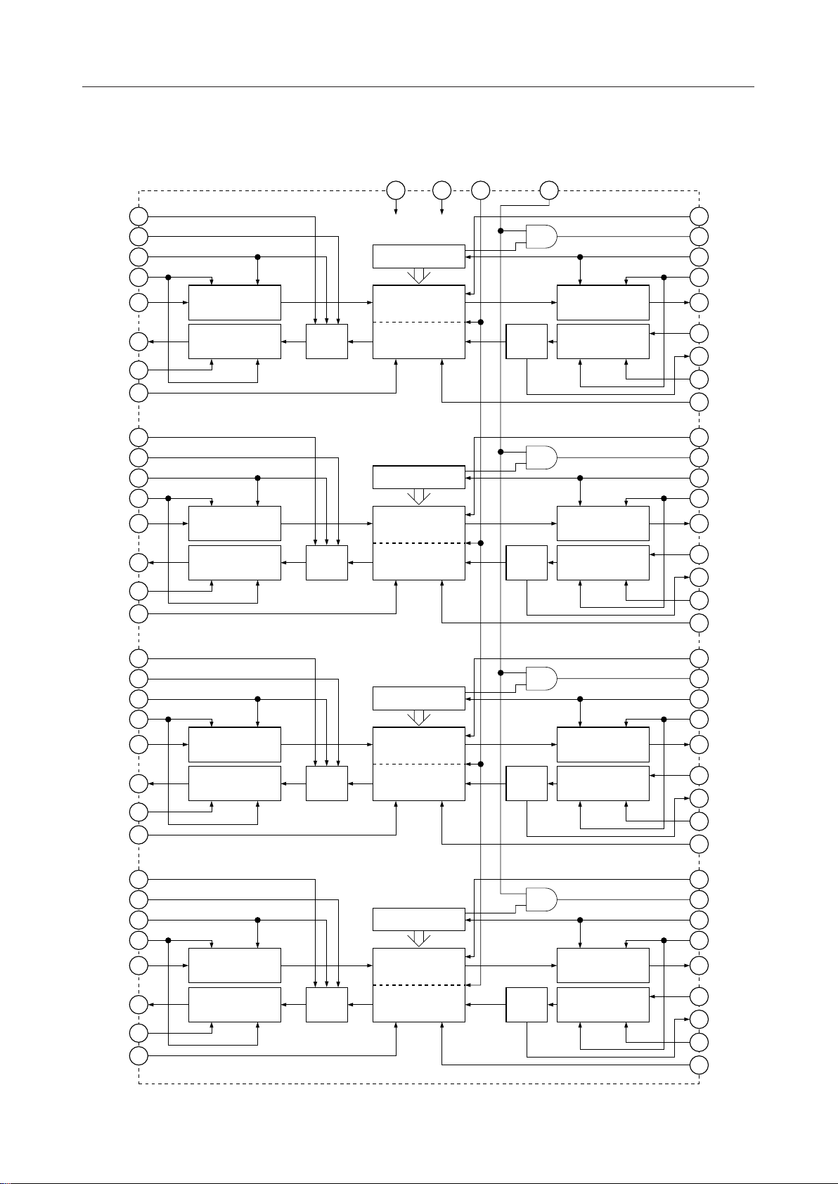
BLOCK DIAGRAM
PAD11
PAD10
SYXP1
BCKP1
SIP1
SOP1
SYRP1
RES1
PAD21
PAD20
SYXP2
BCKP2
SIP2
SOP2
SYRP2
RES2
CODER
S→P
DECODER
S←P
CODER
S→P
DECODER
S←P
+2.7 V to 5.5 V
PAD/
MUTE
PAD/
MUTE
V
DD
PLL
CODER
DECODER
PLL
CODER
DECODER
0 V
MCK
MCK
LAW
PLCKENGND
"0000"
DETECT
"0000"
DETECT
CODER
P→S
DECODER
P←S
CODER
P→S
DECODER
P←S
THR1
PLCK1
SYXA1
BCKA1
SOA1
SIA1
DET1
SYRA1
PDN1
THR2
PLCK2
SYXA2
BCKA2
SOA2
SIA2
DET2
SYRA2
PDN2
PAD31
PAD30
SYXP3
BCKP3
SIP3
SOP3
SYRP3
RES3
PAD41
PAD40
SYXP4
BCKP4
SIP4
SOP4
SYRP4
RES4
CODER
S→P
DECODER
S←P
CODER
S→P
DECODER
S←P
PAD/
MUTE
PAD/
MUTE
PLL
MCK
CODER
DECODER
PLL
MCK
CODER
DECODER
"0000"
DETECT
"0000"
DETECT
CODER
P→S
DECODER
P←S
CODER
P→S
DECODER
P←S
THR3
PLCK3
SYXA3
BCKA3
SOA3
SIA3
DET3
SYRA3
PDN3
THR4
PLCK4
SYXA4
BCKA4
SOA4
SIA4
DET4
SYRA4
PDN4
2/18
Page 3
¡ Semiconductor MSM7581
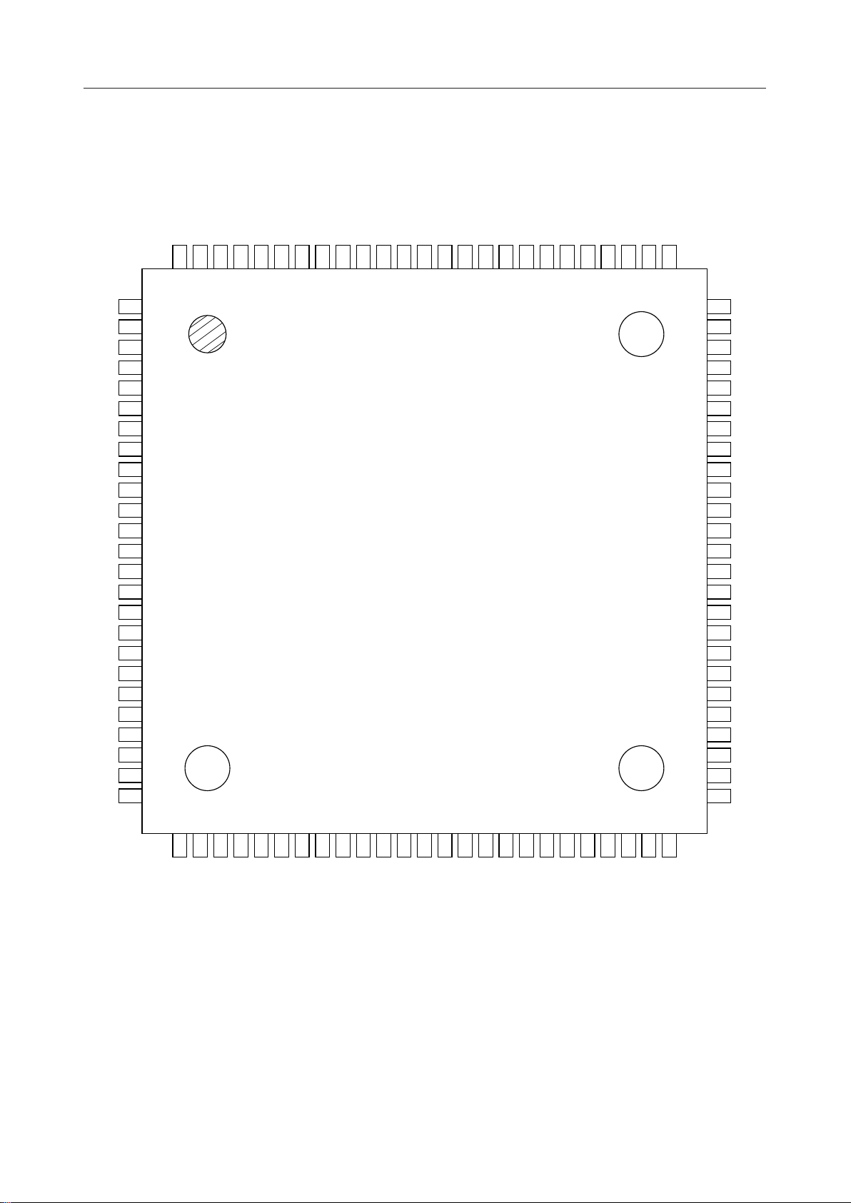
PIN CONFIGURATION (TOP VIEW)
NC
THR1
PLCK1
SYXA1
SOA1
SIA1
NC
DET1
SYRA1
BCKA1
NC
PDN1
NC
PDN2
NC
BCKA2
SYRA2
DET2
NC
SIA2
SOA2
SYXA2
PLCK2
THR2
NC
10
11
12
13
14
15
16
17
18
19
20
21
22
23
24
25
89
DD
V
PLCKENNCPAD41
88
87
86
85
PAD40
SYXP4NCBCKP4
84
83
82
81
SOP4
80
SIP4
79
SYRP4
RES4
78
77
NC
76
75
74
73
72
71
70
69
68
67
66
65
64
63
62
61
60
59
58
57
56
55
54
53
52
51
NC
THR4
PLCK4
SYXA4
SOA4
SIA4
NC
DET4
SYRA4
BCKA4
NC
PDN4
NC
PDN3
NC
BCKA3
SYRA3
DET3
NC
SIA3
SOA3
SYXA3
PLCK3
THR3
NC
NC
RES1
SYRP1
SIP1
SOP1
BCKP1NCSYXP1
99
98
97
96
100
1
2
3
4
5
6
7
8
9
95
94
93
PAD10
PAD11NCGND
92
91
90
262728
NC
RES2
SYRP2
29
SIP2
30
31
SOP2
BCKP2NCSYXP2
32
33
34
35
36
37
DD
NC
V
PAD20
PAD21
NC : No connect pin
100-Pin Plastic TQFP
38
GND
39
LAW
40
NC
41
PAD31
42
43
PAD30
SYXP3NCBCKP3
44
45
46
SOP3
47
SIP3
48
49
RES3
SYRP3
50
NC
3/18
Page 4

¡ Semiconductor MSM7581
PIN AND FUNCTIONAL DESCRIPTIONS
GND
Ground, 0 V.
SIP1, SOP1
PCM serial data input (SIP1) and output (SOP1) for Channel 1.
SOP1 is an open-drain output, which goes into a high impedance state after a continuous 8-bit
serial data output.
SIP2, SOP2
PCM serial data input (SIP2) and output (SOP2) for Channel 2.
SOP2 is an open-drain output, which goes into a high impedance state after a continuous 8-bit
serial data output.
SIP3, SOP3
PCM serial data input (SIP3) and output (SOP3) for Channel 3.
SOP3 is an open-drain output, which goes into a high impedance state after a continuous 8-bit
serial data output.
SIP4, SOP4
PCM serial data input (SIP4) and output (SOP4) Channel 4.
SOP4 is an open-drain output, which goes into a high impedance state after a continuous 8-bit
serial data output.
PAD10 - PAD40, PAD11 - PAD41
PAD mode control.
The PCM output can be attenuated by 12 dB or 6 dB and set to an out-of-service pattern (idle
pattern) by controlling these pins. Set these pins to digital "0" level during normal operation.The
control sequences are as follows:
PAD11 - PAD41 PAD10 - PAD40
00
01
10
11
Normal
6 dB Loss
12 dB Loss
Out-of-service Pattern
4/18
Page 5

¡ Semiconductor MSM7581
THR1, THR2, THR3, THR4
Control pins for the data-through modes.
THR (1 - 4) are for Channel (1 - 4), respectively. The data-through mode is selected when digital
“1” is applied to THR (1 - 4). In this mode, 8-bit serial input data applied to SIA (1 - 4) (ADPCM
data input) is passed to the PCM serial data output pins, SOP (1 - 4), without any data
modification. SOP (1 - 4) go to the high impedance state after the output of 8-bit data has been
applied to SIA (1 - 4).
Conversely 8-bit serial input data applied to SIP (1 - 4) (PCM data input) is passed to ADPCM
serial data output pins, SOA (1 - 4), without any data modification.
SOA (1 - 4) go to the high impedance state after the output of 8-bit serial data has been applied
to SIP (1 - 4).
ADPCM and PCM data interfaces have the mutually independent signal input pins for
synchronizing signals. The time slots for data input and output can be exchanged between them.
Some timing at which data may be deleted or duplicated as described in "Note on Usage" should
not be used.
SYXP1 - 4, SYRP1 - 4
Synchronous signal input pins to define PCM data input and output timing for Channel 1 (SIP1,
SOP1), Channel 2 (SIP2, SOP2), Channnel 3 (SIP3, SOP3), and Channel 4 (SIP4, SOP4).
The synchronous signals SYXA1 and SYRAI (Channel 1), SYXA2 and SYRA2 (Channel 2),
SYXA3 and SYRA3 (Channel 3), and SYXA4 and SYRA4 (Channel 4), which define ADPCM data
input and output timing are provided.
PCM and ADPCM data interfaces can be used at a mutually independent timing except some
timing.
Note: When PCM and ADPCM data interfaces are used at a mutually independent timing, the
timing described in "Note on Usage" should not be used.
SYXP signals must be input for PAD signal input processing.
BCKP1 - 4
Bit clock input.
These signals define the PCM data transmission speed at the PCM data input/output terminals.
BCKP (1 - 4) are used for Channel (1 - 4). Since BCKA (1 - 4) defines the data rate of the ADPCM
data interface, the PCM and ADPCM data can be input or output at different speeds.
LAW
PCM data companding law selection.
Digital “1” and “0” correspond to A-law and µ-law, respectively.
PDN1, PDN2, PDN3, PDN4
Power down mode selection.
PDN1 - 4 can be independently set to power down mode. When digital “0” is applied, these pins
are in the power-down mode.
5/18
Page 6

¡ Semiconductor MSM7581
SIA1, SOA1
ADPCM serial data input (SIA1) and output (SOA1) pins for Channel 1.
SOA1 is an open-drain pin and enters to the high impedance state after outputting a continuous
4-bit serial data stream. When the data-through mode is selected, SOA1 enters to the high
impedance state after outputting an 8-bit serial data stream.
SIA2, SOA2
ADPCM serial data input (SIA2) and output (SOA2) pins for Channel 2.
These pins function the same as SIA1 and SOA1.
SIA3, SOA3
ADPCM serial data input (SIA3) and output (SOA3) pins for Channel 3.
These pins function the same as SIA1 and SOA1.
SIA4, SOA4
ADPCM serial data input (SIA4) and output (SOA4) pins for Channel 4.
These pins function the same as SIA1 and SOA1.
SYXA1 - 4 , SYRA1 - 4
SYXA1, SYXA2, SYXA3, and SYXA4 are synchronous signal input pins to define ADPCM data
input and output timings for Channel 1 (SIA1, SOA1), Channel 2 (SIA2, SOA2), Channel 3 (SIA3,
SOA3), and Channel 4 (SIA4, SOA4), respectively.
Therefore, PCM data interfaces can be used at a mutually independent timing except some
timing.
Since master clocks are generated by the internal PLL using SYXA1 to SYXA4, a synchronous
signal should be input to these pins.
Note: When PCM and ADPCM data interfaces are used at a mutually independent timing, the
timing described in "Note on Usage" should not be used.
DET1, DET2, DET3, DET4
Special ADPCM input data pattern detect pins.
When detecting a 4-bit continuous "0" pattern at the ADPCM input pins Channel 1 (SIA1),
Channel 2 (SIA2), Channel 3 (SIA3), and Channel 4 (SIA4), DET (1 - 4) goes from a digital "0" to
a digital "1" state.
A digital "1" is output at the rising edge of the clock. The fourth data bit (LSB) is clocked into the
register by the bit clock (BCKA 1 - 4) and held there until the rising edge in the next time frame.
When detecting the special data pattern in the next time frame, the digital "1" on the pins DET
(1 - 4) is remains.
6/18
Page 7

¡ Semiconductor MSM7581
RES1, RES2, RES3, RES4
Algorithm reset signal input pins for each Channel (1 - 4) .
When digital “0” is applied, the entire transcoder goes to the initial state.
This reset is defined by ITU-T G.721 and is an optional reset.
The reset width (during "L") should be 125 ms or more.
BCKA1 - 4
Bit clock input pins used to define the data transmission speed at the ADPCM interface.
Using these pins, the ADPCM data interface can be defined at a speed other than the PCM data
interface.
V
DD
Power supply.
The device must operate between +2.7 V and +5.5 V.
PLCKEN
Input pin which enables the output of an 8 kHz clock from the PLLs.
This pin generates the internal master clocks. The 8 kHz clocks from the internal PLLs
synchronized with external signals applied to SYXA 1 - 4 are output to PLCK 1 - 4.
Set this pin at digital "0" during normal operation since it is used as the control pin for testing the
IC.
PLCK1 - 4
Output pins of the 8 kHz clock from PLLs.
When PLCKEN = "1", the 8 kHz clock pulses synchronized with external signals are applied to
SYXA1 - 4 outputs. When PLCKEN = "0", "0" level is output to these pins.
7/18
Page 8

¡ Semiconductor MSM7581
ABSOLUTE MAXIMUM RATINGS
Rating UnitConditionSymbolParameter
Power Supply Voltage
Digital Input Voltage
Storage Temperature
V
T
V
DD
DIN
STG
—
—
—
0 to 7
–0.3 to V
–55 to +150
DD
+ 0.3
V
V
°C
RECOMMENDED OPERATING CONDITIONS
Parameter
Power Supply Voltage
Operating Temperature
Digital Input High Voltage
Digital Input Low Voltage
Bit Clock Frequency
Synchronous
signal Frequency
Clock Duty Ratio
Digital Input Rise Time
Digital Input Fall Time
Synchronous signal Timing
CODER
Synchronous signal Timing
DECODER
Synchronous
signal Width
Data Set-up Time
Data Hold Time
Digital Output Load
Symbol
V
DD
Ta
V
IH
V
IL
F
BCLKA
F
BCLKP
F
SYNC
D
C
t
Ir
t
If
t
XS
t
SX
t
RS
t
SR
t
WS
t
DS
t
DH
R
DL
C
DL
Condition
—
—
All digital input pins
BCKA1 - 4
BCKP1 - 4
SYXP1 - 4, SYRP1 - 4
SYXA1 - 4, SYRA1 - 4
BCKA1 - 4, BCKP1 - 4
All Digital Input Pins
BCKP1 - 4 to SYXP1 - 4
SYXA1 - 4 to BCKA1 - 4
BCKA1 - 4 to SYRA1 - 4
SYRP1 - 4 to BCKP1 - 4
SYXP1 - 4, SYRP1 - 4
SYXA1 - 4, SYRA1 - 4
—
—
SOP1 - 4, SOA1 - 4
(Pull-up Resistor)
SOP1 - 4, SOA1 - 4
DET1 - 4, PLCK1 - 4
Min. Typ. Max. Unit
2.7 — 5.5 V
–30 +25 +80 °C
0.45 ¥ V
0—
—VDDV
DD
0.16 ¥ V
DD
32 — 2048 kHz
64 — 2048 kHz
— 8.0 — kHz
30 50 70 %
— — 50 ns
— — 50 ns
100 — — ns
100 — — ns
100 — — ns
100 — — ns
1 BCLK — 100 ms
100 — — ns
100 — — ns
500 — — W
— — 100 pF
V
8/18
Page 9

¡ Semiconductor MSM7581
ELECTRICAL CHARACTERISTICS
DC Characteristics
Parameter
Power Supply Current
Digital Input High Voltage
Digital Input Low Voltage
Input Leakage
Current
Digital
Output High Voltage
Digital
Output Low Voltage
Output Leakage Current
Input Capacitance
AC Characteristics
Parameter Symbol
Digital Output Delay Time
Symbol
I
DD1
I
DD2
V
IH
V
IL
I
IH
I
IL
V
OH
V
OL1
V
OL2
I
OL
C
IN
t
SDX
t
SDR
t
, t
XD1
t
, t
XD2
t
, t
XD3
t
DD1
t
DD2
Condition
Power On Mode: 4 Channels
Power Down Mode: 4 Channels
All Digital Input Pins
All Digital Input Pins
= V
V
DD
I
VI = 0 V
DET1 - 4, PLCK1 - 4 : I
OH
SOA1 - 4, SOP1 - 4, Pull-up ≥ 500 W
DET1 - 4, PLCK1 - 4 : I
SOP1
-
4, SOA1
All Digital Input Pins
Condition
RD1
RD2
RD3
1 LSTTL + 100 pF
Pull-up: 500 W
= –0.4 mA
= 2 mA
OL
-
4
(V
= 2.7 V to 5.5 V, Ta = –30°C to +80°C)
DD
Min. Typ. Max. Unit
—5 8mA
—1050
0.45 ¥ V
DD
—
0.0 — 0.16 ¥ V
V
DD
DD
— — 2.0
—
0.5 ¥ V
—
—VDDV
DD
0.5
0.0 0.2 0.4 V
0.0 0.2 0.4 V
—
—10mA
—5—pF
(V
= 2.7 V to 5.5 V, Ta = –30°C to +80°C)
DD
Min.
0
0
0
0
0
0
0
Typ.
—
—
—
—
—
—
—
Max.
200
200
200
200
200
200
200
mA
V
V
mA
mA
Unit
ns
ns
ns
ns
ns
ns
ns
9/18
Page 10

¡ Semiconductor MSM7581
,,,
TIMING DIAGRAM
CODER
BCKP1 - 4
SYXP1 - 4
SIP1 - 4
BCKA1 - 4
SYXA1 - 4
SOA1 - 4
DECODER
BCKA1 - 4
SYRA1 - 4
SIA1 - 4
BCKP1 - 4
0 1 2 3 4 5 6 7 8 9 10
t
t
XS
SX
t
DStDH
LSBMSB
0 1 2 3 4 5 6 7 8 9 10
t
t
XS
SX
t
SDX
t
XD1
t
XD2
MSB LSB
t
XD3
0 1 2 3 4 5 6 7 8 9 10
t
RS
SR
t
t
DS
DH
t
MSB LSB
0 1 2 3 4 5 6 7 8 9 10
t
RS
SR
t
SYRP1 - 4
SOP1 - 4
t
SDR
t
RD1
MSB
t
RD2
DET ("0000" detection) Output Timing
BCKA1 - 4
SYRA1 - 4
SIA1 - 4
"0000"
DET1 - 4
t
DD1
Note: 4 bit data pattern except "0000"
"0000"
t
RD3
LSB
Note)
t
DD2
10/18
Page 11

¡ Semiconductor MSM7581
PAD Processing Timing
SYXA
BCKA
SIA
78.125ms
Internal 12dBPAD processing Timing
121.09ms
Internal MUTE processing Timing
MSB LSB
78.125ms
78.125ms
PAD10 to PAD40, PAD11 to PAD41 Timings
SYXP
PAD10, 11
Internal PAD
Signal
BCKP
SOP
ts
ts=100ns or more
th
th=100ns or more
MSB LSB
0dB transmit data PAD processing transmit data
0dB transmit data
As mentioned above, PAD and MUTE processings are performed according to the rising edge
of SYXA. Even if BLOCK is not 128 kHz, these processings are performed in the absolute time
counted from the rising edge of SYXA.
The PAD pin must be controlled so as to cover these processings.
The PAD signal is input in the device at the rising edge of SYXP. Therefore, the PAD signal should
be input at ts and th for the rise of SYXP.
11/18
Page 12

¡ Semiconductor MSM7581
THR Processing Timing
Timing Block Diagrams, when CODER and DECODER output data, are shown in the following
figures.
The parallel to serial conversion of the output unit employs a load format and the load point is
at the rising edge of a synchronous signal.
Therefore, input THR signal with respect to SYXA for CODER with timing of satisfying ts and
th conditions shown in the figure.
For DECODER, THR signal should be input even of through-data is input.
The input timing should satisfy the conditions shown in the following figures.
CODER
Through-data
SYXP
SIP
BCKP
Serial
Parallel
8b
Parallel
S
4b
E
L
Serial
8
Latch
ADPCM
CODER
SYNCA
SOA
BCLKA
THR
PCM side SYNC (SYXP)
PCM Input (SIP)
Internal Latch timing (A)
Internal Input Data
ADPCM side SYNC (SYXA)
Through-data Output (SOA)
BCKA
THR
Latch timing=A
MSB LSB
Through-data
MSB
ts
th
ts=100ns or more
th=100ns or more
Note: That data-ship may occur when the rising edge (data load point) of SYXA and input of
the internal latch timing overlap each other.
12/18
Page 13

¡ Semiconductor MSM7581
g
DECODER
Through-data
SYNCA
SIA
BCLKA
Serial
Parallel
8b
Parallel
S
8b
E
L
Serial
8
Latch
ADPCM
DECODER
SYNCP
SOP
BCLKP
THR
ADPCM side SYNC (SYXA)
ADPCM Input (SIA)
Internal Latch timing (A)
Internal Input Data
PCM side SYNC (SYXP)
Throgh-data output (SOP)
BCLKP
THR
Latch timing=A
MSB LSB
Less than are BCLKP cycle
from the risin
edge of SYXA signal.
Through-data
This data is output here.
MSB
100ns or more
13/18
Page 14

¡ Semiconductor MSM7581
APPLICATION CIRCUIT
CODER 4 Side
ADPCM Output
DECODER 4 Side
ADPCM Intput
V
DD
CODER 3 Side
ADPCM Output
DECODER 3 Side
ADPCM Intput
V
DD
8 kHz Synchronous Signal
(Channel 4)
CODER 4 Side
PCM Intput
DECODER 4 Side
PCM Output
GND
DECODER 1 Side
PCM Output
CODER 1 Side
PCM Intput
8 kHz Synchronous Signal
(Channel 3)
75747372717069686766656463626160595857515655545352
NC
76
V
DD
NC
RES4
THR4
PLCK4
SYXA4
SOA4
SIA4
NC
DET4
BCKA4
SYRA4
NC
PDN4
NC
NC
PDN3
BCKA3
SYRP4
SIP4
SOP4
BCKP4
82
NC
83
SYXP4
84
PAD40
85
PAD41
86
NC
87
PLCKEN
88
V
DD
89
GND
90
NC
91
PAD11
92
PAD10
93
V
DD
SYXP1
94
NC
95
BCKP1
96
SOP1
97
SIP1
98
SYRP1
99
RES1
100
NC
NC
THR1
PLCK1
123456789
SYXA1
SOA1
SIA1NCDET1
MSM7581
SYRA1
BCKA1NCPDN1
101112131415161718
NC
PDN2
BCKA2
NC
NC
SIA3
DET3
SYRA3
SIA2
NC
DET2
SYRA2
19252021222324
SOA3
SOA2
PLCK3
SYXA3
PLCK2
SYXA2
THR3
RES3
SYRP3
SIP3
SOP3
BCKP3
SYXP3
PAD30
PAD31
LAW
GND
PAD21
PAD20
SYXP2
BCKP2
SOP2
SIP2
SYRP2
RES2
THR2
NC
50
NC
4977
4878
4779
4680
4581
44
NC
43
42
41
40
NC
39
38
37
V
DD
36
NC
35
34
33
32
NC
31
30
29
28
27
26
NC
V
DD
CODER 3 Side
PCM Intput
DECODER 3 Side
PCM Output
V
DD
V
DD
DECODER 2 Side
PCM Output
CODER 2 Side
PCM Intput
NC
8 kHz Synchronous Signal
(Channel 1)
8 kHz Synchronous Signal
(Channel 2)
V
DD
CODER 1 Side
ADPCM Intput
ADPCM Output
DECODER 1 Side
V
DD
0.1 mF 10 mF
GND
+
-
ADPCM Intput
DECODER 2 Side
V
CODER 2 Side
ADPCM Output
DD
Shift Clock
(Channel 1 - 4)
64 kHz to 2048 kHz
14/18
Page 15

¡ Semiconductor MSM7581
NOTES ON USAGE
(1) Through Mode (CODER Side)
t0 t1
BCLK
12345678
PCM side SYNC (SYXP)
PCM Input (SIP)
Internal Latch Timing
(A)
ADPCM side SYNC (SYXA)
Through-Data Output (SOA)
(B)
ADPCM side SYNC (SYXA)
Through-Data Output (SOA)
PCMDATA1
ADPCMDATA0 ADPCMDATA1 ADPCMDATA2
*t1 is the falling edge of the 8th BCLK counted from t0.
PCMDATA2 PCMDATA3
ADPCMDATA0 ADPCMDATA1
(A) When SYXA rises after t1, PCMDATA1 is output to ADPCMDATA1.
(B) When SYXA rises before t1, PCMDATA1 is output to ADPCMDATA1.
If SYXA rises near the t1 and jitter occurs, data slip may occur. Therefore SYXA should not rise in the range of ±500ns from t1.
The data slip means that data is deleted or the same data is output twice.
(2) Through Mode (DECODER Side)
t0 t1
BCLK
12345678
ADPCM side SYNC (SYRA)
ADPCM Input (SIA)
Internal Latch Timing
(A)
PCM side SYNC (SYRP)
Through-Data Output (SOP)
(B)
PCM side SYNC (SYRP)
Through-Data Output (SOP)
ADPCMDATA1
PCMDATA0 PCMDATA1 PCMDATA2
ADPCMDATA2 ADPCMDATA3
PCMDATA0 PCMDATA1
*t1 is the falling edge of the 8th BCLK counted from t0.
(A) When SYRP rises after t1, ADPCMDATA1 is output to PCMDATA1.
(B) When SYRP rises before t1, ADPCMDATA1 is output to PCMDATA1.
If SYRP rises near the t1 and jitter occurs, data slip may occur. Therefore SYRP should not rise in the range of ±500ns from t1.
The data slip means that data is deleted or the same data is output twice.
15/18
Page 16

¡ Semiconductor MSM7581
(3) PCMÆADPCM, ADPCMÆPCM during Transcode
(a) CODER Timing Diagram
t0
SYXA
SYXP
BCKP
SIP
Internal (1)
Timing (2)
Timing (3)
SOA
123456
MSB
(b) DECODER Timing Diagram
SYRA
BCKA
SIA
Internal (6)
SYRP
Timing (4)
Timing (5)
SOP
MSB
LSB
78
LSB
PCM Input Data
Tsip t4
104.2ms
119.8ms
MSB LSBLSB MSB
Tsoa
1234
MSB LSB MSB
ADPCM Input Data
Tsia
Tsop
65.2ms
119.8ms
t6
t7
t3
A
t1
t2
t5
B
t2
PCM Output Data
t4 is the falling edge of the 8th BCLK
*
counted from the rising edge of SYXP.
* t5 is the rising edge of SYXA.
* t6 is the falling edge of the 4th BCLK
counted from the rising edge of SYRA.
* t7 is the rising edge of SYRP.
(c) Internal Circuit Configuration
SIP
SYXP
BCKP
SOP
S
8bit
/
P
P
8bit
/
S
(1)
Latch
(2)
(5)
Latch
From
DECODERToDECODER
From CODER
PLL
SYXA
(3)
(4)
Latch
Latch
8bitTo CODER
(6)
8bit
P
/
SOA
SYXA
S
BCKA
S
/
P
SYRASYRP
SIA
16/18
Page 17

¡ Semiconductor MSM7581
In this device, internal operating signals are generated according to the ADPCM side SYNC
(SYXA) signal.
The timings are shouwn in the figures (a) and (b);
The arithmetic operation of CODER is performed at "A" in the figure (a).
The arithmetic operation of DECODER is performed at "B" in the figure (b).
Therefore, when the conversion delay time Tsip of the CODER is less than t1, ADPCM is output
at the timing of Tsoa.
When Tsip is more than t1, ADPCM is output at the timing of Tsoa + 125ms.
For DECODER, when Tsia<t3 and Tsop<t2, the conversion delay time is Tsop-Tsia.
As mentioned above, a data ship may occur at Tsip=t1 in CODER, and at Tsia=t3 and Tsop=t2
in DECODER.
Therefore, the timings of SYNC signals of both PCM and ADPCM sides should not be set up in
the range about ±500nsec of Tsip=t1, Tsia=t3 and Tsop=t2.
For normal operation, SYNC clocks for ADPCM and PCM sides should be continuous at 8 kHz
and synchronized with each other even if their phases are different.
17/18
Page 18

¡ Semiconductor MSM7581
PACKAGE DIMENSIONS
(Unit : mm)
TQFP100-P-1414-0.50-K
Mirror finish
Package material
Lead frame material
Pin treatment
Solder plate thickness
Package weight (g)
Epoxy resin
42 alloy
Solder plating
5 mm or more
0.55 TYP.
Notes for Mounting the Surface Mount Type Package
The SOP, QFP, TSOP, SOJ, QFJ (PLCC), SHP and BGA are surface mount type packages, which
are very susceptible to heat in reflow mounting and humidity absorbed in storage.
Therefore, before you perform reflow mounting, contact Oki’s responsible sales person for the
product name, package name, pin number, package code and desired mounting conditions
(reflow method, temperature and times).
18/18
 Loading...