

Page 1

E2U0031-39-61
¡ Semiconductor MSM7580
¡ Semiconductor
This version: Jun. 1999
Previous version: Aug. 1998
MSM7580
ITU-T G.721 ADPCM TRANSCODER
GENERAL DESCRIPTION
The MSM7580 is an ADPCM transcoder which is used by the new digital cordless system. It
converts 64 kbps voice PCM serial data to 32 kbps ITU-T G.721 ADPCM serial data, and vice
versa.
This device consists of two systems with full-duplex voice data channels and a data-through
mode.
The MSM7580 provides cost effective solutions for digital cordless office telephone systems
which are incorporated into PABXs and for the public base stations which are connected to the
central office through digital PSTNs.
FEATURES
• Conforms to ITU-T G.721
• Built-in Full-duplex Transcoder with Two Data channels
• PCM companding Law: A-law/µ-law selectable
• Synchronized Operation between coder and decoder, and between two channels.
• Serial PCM Data Transmission Speed: 64 kbps to 2048 kbps
• Serial ADPCM Data Transmission Speed: 32 kbps to 2048 kbps
• Hardware Reset – ITU-T G.721 Optional Reset – for each channel
• Power Down Control for each channel
• Decoder (ADPCM Æ PCM ) MUTE Mode and PAD Mode for each channel
• ADPCM Data-through Mode
• Capable of time slot conversion
• Special ADPCM Input Data Code (”0000”) Detector for each channel
• Master Clock Signal : Not necessary
• Power supply voltage/Consumption current :
+5 V ±10%, 2.5 mA/channel
• Package :
28-pin plastic SOP (SOP28-P-430-1.27-K) (Product name : MSM7580GS-K)
1/17
Page 2
2/17
¡ Semiconductor MSM7580
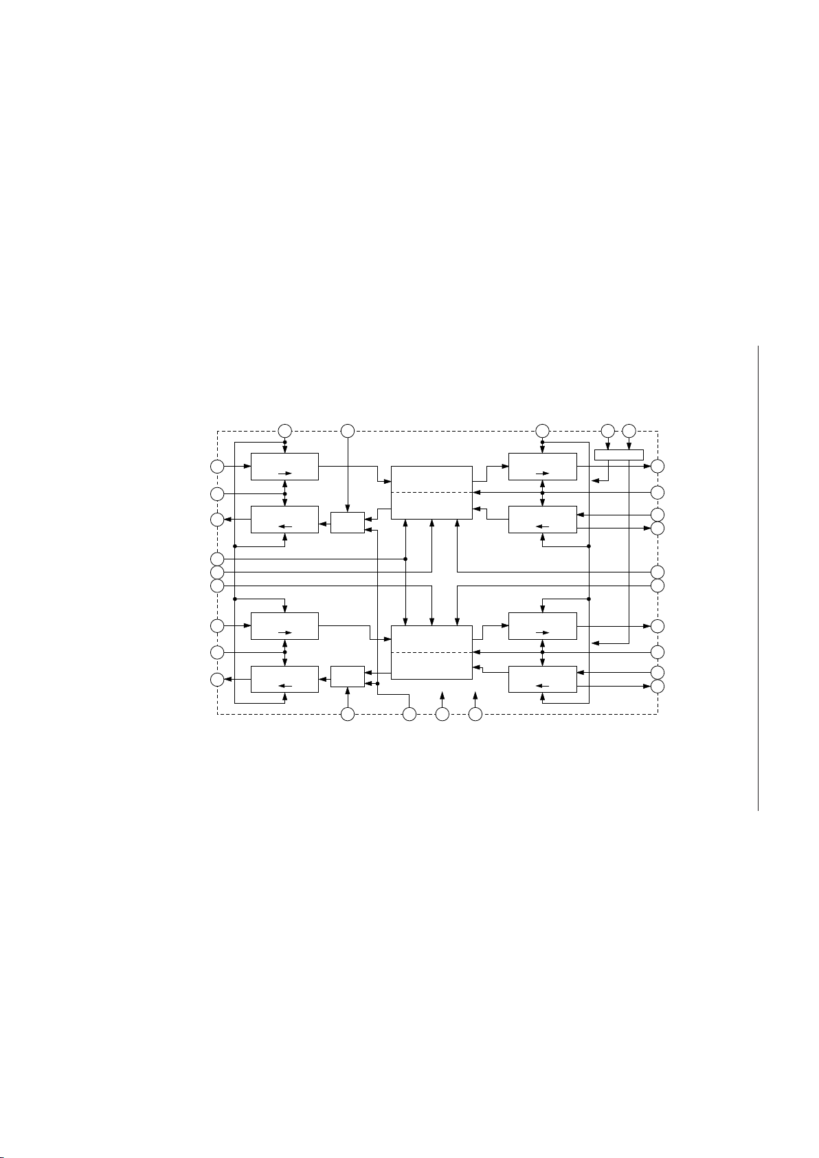
BLOCK DIAGRAM
SIP1
SYNCP1
SOP1
LAW
THR1
THR2
SIP2
SYNCP2
SOP2
SIA2
SYNCA2
SOA2
DET2
RES2
RES1
DET1
SIA1
SYNCA1
SOA1
BCLKP MUTE1 BCLKA PDN1 PDN2
MUTE2 PAD/
MUTE
VDDGND
CODER
P S
DECODER
P S
DECODER
P S
CODER
P S
CODER
DECODER
CODER
DECODER
CODER
S P
DECODER
S P
DECODER
S P
CODER
S P
MUTE
/
PAD
+5 V 0 V
MUTE
/
PAD
POWER DOWN
Page 3
¡ Semiconductor MSM7580
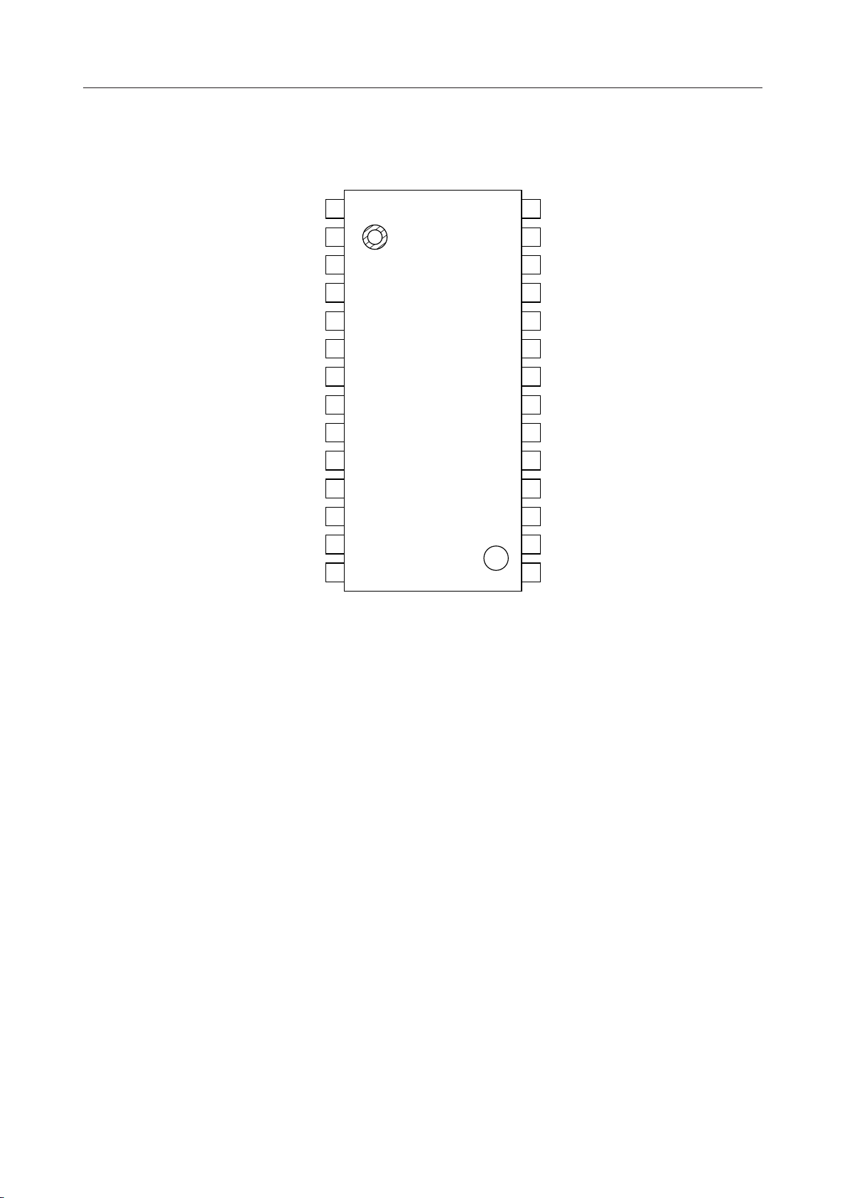
PIN CONFIGURATION (TOP VIEW)
SIP2
SOP2
THR2
MUTE2
SYNCP2
PAD/MUTE
BCLKP
GND
LAW
SYNCP1
MUTE1
THR1
SOP1
SIP1
1
2
3
4
5
6
7
8
9
10
11
12
13
14
28-Pin Plastic SOP
28
27
26
25
24
23
22
21
20
19
18
17
16
15
SOA2
SIA2
SYNCA2
RES2
DET2
PDN2
V
DD
BCLKA
PDN1
DET1
RES1
SYNCA1
SIA1
SOA1
3/17
Page 4

¡ Semiconductor MSM7580
PIN AND FUNCTIONAL DESCRIPTIONS
GND
Ground, 0 V.
SIP1, SOP1
PCM serial data input (SIP1) and output (SOP1) for Channel 1.
SOP1 is an open-drain output, which goes into a high impedance state after a continuous 8-bit
serial data output.
SIP2, SOP2
PCM serial data input (SIP2) and output (SOP2) for Channel 2.
SOP2 is an open-drain output, which goes into a high impedance state after a continuous 8-bit
serial data output.
PAD/ MUTE
Control input for the selection of PAD or MUTE mode.
When digital "1" is input, the PAD mode is selected and when digital "0" is input, the MUTE mode
is selected.
THR1, THR2
Control pins for the data through modes.
THR1 and THR2 are for Channel 1 and Channel 2, respectively. The data-through mode is
selected when digital “1” is applied to THR1 and THR2. In this mode, 8-bit serial input data
applied to SIA1 and SIA2 (ADPCM data input) is passed to the PCM serial data output pins,
SOP1 and SOP2, without any data modification. SOP1 and SOP2 go to the high impedance state
after the output of 8-bit data has been applied to SIA1 and SIA2.
Conversely 8-bit serial input data applied to SIP1 and SIP2 (PCM data input) is passed to
ADPCM serial data output pins, SOA1 and SOA2, without any data modification.
SOA1 and SOA2 go to the high impedance state after the output of 8-bit data has been applied
to SIP1 and SIP2.
Since ADPCM and PCM data interfaces have the mutually independent signal input pins for
synchronizing signals the time slots for data input and output can be exchanged between them.
Some timing at which data may be deleted or duplicated as described in "Notes on Usage" should
not be used.
MUTE1, MUTE2
Setting a digital "1"at these pins sets the PCM output to the idle pattern state regardless of the
ADPCM input data, when the MUTE mode is selected by the PAD/MUTE pin.
When the PAD mode is selected, the PCM output has a 12 dB loss.
Normally, these pins are set to a digital "0".
When the data through mode is selected, the function of these pins is invalid.
4/17
Page 5

¡ Semiconductor MSM7580
SYNCP1, SYNCP2
Synchronous signal input.
SYNCP1 and SYNCP2 control the PCM data input/output timing for Channel 1 (SIP1, SOP1)
and Channel 2 (SIP2, SOP2), respectively.
Since other synchronous signal input pins SYNCA1 and SYNCA 2 for ADPCM interfaces are also
provided, the PCM and ADPCM data can be input or output with different timing.
PCM and ADPCM data interfaces can be used at a mutually independent timing except same
timing.
Note: When PCM and ADPCM data interfaces are used at a mutually independent timing, the
timing described in "Notes on Usage" should not be used.
BCLKP
Bit clock input.
This signal defines the PCM data transmission speed at the PCM data input/output pins.
BCLKP is used for Channels 1 and 2. Since BCLKA defines the data rate of the ADPCM data
interface, the PCM and ADPCM data can be input or output at different speeds.
LAW
PCM data companding law (A-law/m-law) selection.
Digital “1” and “0” correspond to A-law and µ-law, respectively.
PDN1, PDN2
Power down mode selection.
PDN1 and PDN2 can be independently set to power down mode. When a digital “0” is applied,
these pins are in the power-down mode.
SIA1, SOA1
ADPCM serial data input (SIA1) and output (SOA1) pins for Channel 1.
SOA1 is an open-drain pin and enters to the high impedance state after outputting a continuous
4-bit serial data stream. When the data-through mode is selected, SOA1 enters to the high
impedance state after outputting an 8-bit serial data stream.
SIA2, SOA2
ADPCM serial data input (SIA2) and output (SOA2) pins for Channel 2.
These pins function the same as SIA1 and SOA1.
5/17
Page 6

¡ Semiconductor MSM7580
SYNCA1 , SYNCA2
Synchronous signal input pins.
SYNCA1 and SYNCA 2 control the ADPCM data input/output timing for Channel 1 (SIA1,
SOA1) and Channel 2 (SIA2, SOA2), respectivery.
The ADPCM data can be input or output with timing other than the PCM data interface.
Therefore PCM and ADPCM interfaces can be used at a mutually independent timing except
some timing.
Since master clocks are generated by the internal PLL using SYNCA, a synchronous signal
should be input to there pins.
Note: When PCM and ADPCM data interfaces are used at a mutually independent timing, the
timing described in "Notes on Usage" should not be used.
DET1, DET2
Special ADPCM input data pattern detect pins.
When a 4-bit continuous "0" pattern at the ADPCM input pins Channel 1 (STA1) and Channel 2
(SIA2) is detected, DET1 and DET2 go from a digital "0" to a digital "1" state.
A digital "1" is output at the rising edge of the clock.
The fourth data bit (LSB) is clocked into the register by the bit clock (BCLKA) and the held there
until the rising edge in the next time frame.
When detecting the special data pattern in the next time frame, the digital "1" on the pins DET
(1, 2) is remains. When the THR1 pin or THR2 pin is at digital "1" level, the functions of these pins
are invalid.
RES1, RES2
Algorithm reset signal input pins for Channel 1 (RES1) and Channel 2 (RES2).
When a digital “0” is applied, the entire transcoder goes to its initial state.
This reset is defined by ITU-T G.721 and is an optional reset.
BCLKA
Bit clock input pin used to define the data transmission speed at the ADPCM interface.
This pin can be used for Channels 1 and 2, which allows the ADPCM data interface speed to be
defined differently than the PCM data interface speed.
V
DD
Power supply.
The device must operate at +5 V ±10%.
6/17
Page 7

¡ Semiconductor MSM7580
ABSOLUTE MAXIMUM RATINGS
Parameter
Power Supply Voltage
Digital Input Voltage
Storage Temperature
Symbol
V
DD
V
DIN
T
STG
Condition Rating Unit
—
—
—
RECOMMENDED OPERATING CONDITIONS
Parameter
Power Supply Voltage
Operating Temperature
Digital Input High Voltage
Digital Input Low Voltage
Bit Clock Frequency
Synchronous
Signal Frequency
Clock Duty Ratio
Digital Input Rise Time
Digital Input Fall Time
Synchronous Signal Timing
CODER
Synchronous Signal Timing
DECODER
Synchronous
Signal Width
Data Set-up Time
Data Hold Time
Digital Output Load
Symbol
V
DD
Ta
V
IH
V
IL
F
BCLKA
F
BCLKP
F
SYNC
D
C
t
Ir
t
If
t
XS
t
SX
t
SX
t
SR
t
WS
t
DS
t
DH
R
DL
C
DL
SOP1, SOP2, SOA1, SOA2,
Condition
—
—
All Digital Input Pins
BCLKA
BCLKP
SYNCP1, SYNCP2,
SYNCA1, SYNCA2
BCLKA, BCLKP
All Digital Input Pins
BCLKA, BCLKP to SYNCP
SYNCP to BCLKA, BCLKP
BCLKA, BCLKP to SYNCA
SYNCA to BCLKA, BCLKP
SYNCP1, SYNCP2,
SYNCA1, SYNCA2
—
—
SOP1, SOP2, SOA1, SOA2
(Pull-up Resistor)
DET1, DET2
–0.3 to V
–55 to +150
Min.
4.5
–30
2.2
0
32
64
—
30
—
—
100
100
100
100
1 BCLK
100
100
500
—
0 to 7
DD
Typ.
+ 0.3
—
+25
—
—
—
—
8.0
50
—
—
—
—
—
—
—
—
—
—
—
Max.
5.5
+80
V
DD
0.6
2048
2048
—
70
50
50
—
—
—
—
100
—
—
—
100
V
V
°C
Unit
V
°C
V
V
kHz
kHz
kHz
%
ns
ns
ns
ns
ns
ns
ms
ns
ns
W
pF
7/17
Page 8

¡ Semiconductor MSM7580
ELECTRICAL CHARACTERISTICS
DC Characteristics
(V
= 4.5 V to 5.5 V, Ta = –30°C to +80°C)
DD
Parameter
Power Supply Current
Input High Voltage
Input Low Voltage
Input Leakage
Current
Digital
Output High Voltage
Digital
Output Low Voltage
Output Leakage Current
Input Capacitance
Symbol
I
DD1
I
DD2
V
IH
V
IL
I
IH
I
IL
V
OH
V
OL1
V
OL2
I
OL
C
IN
Condition
Power On Mode: 2 Channels
Power Down Mode: 2 Channels
—
—
= V
V
I
DD
VI = 0 V
DET1, DET2 : I
= –0.4 mA
OH
1 LSTTL, Pull-up : 500 W
DET1, DET2 : I
= 1.6 mA
OL
SOP1, SOP2, SOA1, SOA2
—
Min.
—
—
2.2
0.0
—
—
2.8
0.0
0.0
—
—
Typ
5
0.1
—
—
—
—
—
0.2
0.2
—
5
Max.
10
0.2
V
DD
0.6
2.0
0.5
V
DD
0.4
0.4
10
—
Unit
mA
mA
V
V
mA
mA
V
V
V
mA
pF
AC Characteristics
Parameter
Digital Output Delay Time
Symbol
t
SDX
t
SDR
t
, t
XD1
RD1
t
, t
XD2
RD2
t
, t
XD3
RD3
t
DD1
t
DD2
Condition
1 LSTTL + 100 pF
Pull-up: 500 W
(V
= 4.5 V to 5.5 V,Ta = –30°C to +80°C)
DD
Min. Typ.
0
0
0
0
0
0
0
—
—
—
—
—
—
—
Max. Unit
200
200
200
200
200
200
200
ns
ns
ns
ns
ns
ns
ns
8/17
Page 9

¡ Semiconductor MSM7580
,,,
TIMING DIAGRAM
CODER
BCLKP
SYNCP
SIP
BCLKA
SYNCA
SOA
DECODER
BCLKA
SYNCA
SIA
BCLKP
0 1 2 3 4 5 6 7 8 9 10
t
t
XS
SX
t
DStDH
LSBMSB
0 1 2 3 4 5 6 7 8 9 10
t
t
XS
SX
t
SDX
t
XD1
t
XD2
MSB LSB
t
XD3
0 1 2 3 4 5 6 7 8 9 10
t
RS
SR
t
t
DS
DH
t
MSB LSB
0 1 2 3 4 5 6 7 8 9 10
t
RS
SR
t
SYNCP
SOP
t
SDR
t
RD1
MSB
t
RD2
DET ("0000" detection) Output Timing
BCLKA
SYNCA
SIA
"0000"
DET
t
DD1
Note: 4-bit data pattern except "0000"
"0000"
t
RD3
LSB
Note)
t
DD2
9/17
Page 10

¡ Semiconductor MSM7580
)
PAD/MUTE Processing Timing
SYNCA
BCLKA
SIA
78.125ms
Internal 12dBPAD Processing Timing
121.09ms
Internal MUTE Processing Timing
MSB LSB
78.125ms
78.125ms
PAD Mode; MUTE1 and MUTE 2 Timings PAD/MUTE="H"
MUTE1, 2
SYNCP
BCLKP
SOP
MSB LSB
0dB transmit data 12dB loss transmit data
0dB transmit data
MUTE Mode; MUTE1 and MUTE 2 Timings PAD/MUTE="L"
MUTE1, 2
SYNCP
BCLKP
SOP
MSB LSB
0dB transmit data MUTE (idle channel state
0dB transmit data
As mentioned above, PAD and MUTE processings are carried out according to the rising edge
of SYNCA.
Even if BCLK is not 128 kHz, these processings are performed in the absolute time counted from
the rising edge of SYNCA.
Therefore, MUTE1 and MUTE 2 pins must be controlled so as to cover there processsings.
10/17
Page 11

¡ Semiconductor MSM7580
THR Processing Timing
Timing Block Diagrams, when CODER and DECODER output data, are shown in the following
figures.
The parallel to serial conversion of the output unit employs a load format and the load point is
at the rising edge of a synchronous signal.
Therefore, input THR signal with respect to SYNCA for CODER with timing of satisfying ts and
th conditions shown in the figure.
For DECODER, THR signal should be input even when through-data is input.
The input timing should satisfy the conditions shown in the following figures.
CODER
Through-data
SYNCP
SIP
BCLKP
Serial
Parallel
8b
Parallel
S
4b
E
L
Serial
8
Latch
ADPCM
CODER
SYNCA
SOA
BCLKA
THR
PCM side SYNC (SYNCP)
PCM Input (SIP)
Internal Latch timing (A)
Internal Input Data
ADPCM side SYNC (SYNCA)
Through-data Output (SOA)
BCLKA
THR
Latch timing=A
MSB LSB
Through-data
MSB
ts
th
ts=100ns or more
th=100ns or more
Note: That data-ship may occur when the rising edge (data load point) of SYNCA and input of
the internal latch timing overlap each other.
11/17
Page 12

¡ Semiconductor MSM7580
g
DECODER
Through-data
SYNCA
SIA
BCLKA
Serial
Parallel
8b
Parallel
S
8b
E
L
Serial
8
Latch
ADPCM
DECODER
SYNCP
SOP
BCLKP
THR
ADPCM side SYNC (SYNCA)
ADPCM Input (SIA)
Internal Latch timing (A)
Internal Input Data
PCM side SYNC (SYNCP)
Throgh-data output (SOP)
BCLKP
THR
Latch timing=A
MSB LSB
Less than are BCLKP cycle
from the risin
edge of SYNCA signal.
Through-data
This data is output here.
MSB
100ns or more
12/17
Page 13

¡ Semiconductor MSM7580
APPLICATION CIRCUIT
CODER2
PCM Input
DECODER2
PCM Output
8 kHz SYNC SIGNAL
(Channel2)
Shift Clock
(Channel1, 2)
(64 kHz to 2048 kHz)
8 kHz SYNC SIGNAL
(Channel1)
DECODER1
PCM Output
V
DD
V
DD
MSM7580GS-K
CODER2
GND
SIP2
SOP2
THR2
MUTE2
SYNCP2
PAD/MUTE
BCLKP
GND
LAW
SYNCP1
SOA2
SIA2
SYNCA2
RES2
DET2
PDN2
V
DD
BCLKA
PDN1
DET1
ADPCM Output
DECODER2
ADPCM Input
V
DD
MUTE1 RES1
THR1 SYNCA1
SOP1 SIA1
DECODER1
ADPCM Input
CODER1
PCM Input
SIP1 SOA1
V
DD
GND
CODER1
ADPCM Output
+
10 mF1 mF
–
13/17
Page 14

¡ Semiconductor MSM7580
NOTES ON USAGE
(1) Through Mode (CODER Side)
t0 t1
BCLK
12345678
PCM side SYNC (SYNCP)
PCM Input (SIP)
Internal Latch Timing
(A)
ADPCM side SYNC (SYNCA)
Through-Data Output (SOA)
(B)
ADPCM side SYNC (SYNCA)
Through-Data Output (SOA)
PCMDATA1
ADPCMDATA0 ADPCMDATA1 ADPCMDATA2
*t1 is the falling edge of the 8th BCLK counted from t0.
PCMDATA2 PCMDATA3
ADPCMDATA0 ADPCMDATA1
(A) When SYNCA rises after t1, PCMDATA1 is output to ADPCMDATA1.
(B) When SYNCA rises before t1, PCMDATA1 is output to ADPCMDATA1.
If SYNCA rises near the t1 and jitter occurs, data slip may occur. Therefore SYNCA should not rise in the range of ±500ns from t1.
Data slip means that data is deleted or the same data is output twice.
(2) Through Mode (DECODER Side)
t0 t1
BCLK
12345678
ADPCM side SYNC (SYNCA)
ADPCM Input (SIA)
Internal Latch Timing
(A)
PCM side SYNC (SYNCP)
Through-Data Output (SOP)
(B)
PCM side SYNC (SYNCP)
Through-Data Output (SOP)
ADPCMDATA1
PCMDATA0 PCMDATA1 PCMDATA2
ADPCMDATA2 ADPCMDATA3
PCMDATA0 PCMDATA1
*t1 is the falling edge of the 8th BCLK counted from t0.
(A) When SYNCA rises after t1, ADPCMDATA1 is output to PCMDATA1.
(B) When SYNCA rises before t1, ADPCMDATA1 is output to PCMDATA1.
If SYNCP rises near the t1 and jitter occurs, data slip may occur. Therefore SYNCA should not rise in the range of ±500ns from t1.
Data slip means that data is deleted or the same data is output twice.
14/17
Page 15

¡ Semiconductor MSM7580
(3) PCMÆADPCM, ADPCMÆPCM during Transcode
(a) CODER Timing Diagram
t0
SYNCA
SYNCP
BLCKP
SIP
Internal (1)
Timing (2)
Timing (3)
SOA
123456
MSB
(b) DECODER Timing Diagram
SYNCA
BCLKA
SIA
Internal (6)
SYNCP
Timing (4)
Timing (5)
SOP
MSB
LSB
78
LSB
PCM Input Data
Tsip t4
104.2ms
119.8ms
MSB LSBLSB MSB
Tsoa
1234
MSB LSB MSB
ADPCM Input Data
Tsia
Tsop
65.2ms
119.8ms
t6
t7
t3
A
t1
t2
t5
B
t2
PCM Output Data
t4 is the falling edge of the 8th BCLK
*
counted from the rising edge of SYNCP.
* t5 is the rising edge of SYNCA.
* t6 is the falling edge of the 4th BCLK
counted from the rising edge of SYNCA.
* t7 is the rising edge of SYNCP.
(c) Internal Circuit Configuration
SIP
SYNCP
BCLKP
SOP
(1)
S
8bit
/
P
P
8bit
/
S
Latch
(2)
(5)
Latch
From
DECODERToDECODER
From CODER
PLL
SYNCA
(3)
(4)
Latch
Latch
8bitTo CODER
(6)
8bit
P
/
SOA
SYNCA
S
BCLKA
S
/
P
SIA
15/17
Page 16

¡ Semiconductor MSM7580
In this device, internal operating signals are generated according to the ADPCM side SYNC
(SYNCA) signal.
The timings are shouwn in the figures (a) and (b);
The arithmetic operation of CODER is performed at "A" in the figure (a).
The arithmetic operation of DECODER is performed at "B" in the figure (b).
Therefore, when the conversion delay time Tsip of the CODER is less than t1, ADPCM is output
at the timing of Tsoa.
When Tsip is more than t1, ADPCM is output at the timing of Tsoa + 125ms.
For DECODER, when Tsia<t3 and Tsop<t2, the conversion delay time is Tsop-Tsia.
As mentioned above, a data ship may occur at Tsip=t1 in CODER, and at Tsia=t3 and Tsop=t2
in DECODER.
Therefore, the timings of SYNC signals of both PCM and ADPCM sides should not be set up in
the range about ±500nsec of Tsip=t1, Tsia=t3 and Tsop=t2.
For normal operation, SYNC clocks for ADPCM and PCM sides should be continuous at 8 kHz
and synchronized with each other even if their phases are different.
16/17
Page 17

¡ Semiconductor MSM7580
PACKAGE DIMENSIONS
(Unit : mm)
SOP28-P-430-1.27-K
Mirror finish
Package material
Lead frame material
Pin treatment
Solder plate thickness
Package weight (g)
Epoxy resin
42 alloy
Solder plating
5 mm or more
0.75 TYP.
Notes for Mounting the Surface Mount Type Package
The SOP, QFP, TSOP, SOJ, QFJ (PLCC), SHP and BGA are surface mount type packages, which
are very susceptible to heat in reflow mounting and humidity absorbed in storage.
Therefore, before you perform reflow mounting, contact Oki’s responsible sales person for the
product name, package name, pin number, package code and desired mounting conditions
(reflow method, temperature and times).
17/17
Page 18

E2Y0002-29-11
NOTICE
1. The information contained herein can change without notice owing to product and/or
technical improvements. Before using the product, please make sure that the information
being referred to is up-to-date.
2. The outline of action and examples for application circuits described herein have been
chosen as an explanation for the standard action and performance of the product. When
planning to use the product, please ensure that the external conditions are reflected in the
actual circuit, assembly, and program designs.
3. When designing your product, please use our product below the specified maximum
ratings and within the specified operating ranges including, but not limited to, operating
voltage, power dissipation, and operating temperature.
4. Oki assumes no responsibility or liability whatsoever for any failure or unusual or
unexpected operation resulting from misuse, neglect, improper installation, repair, alteration
or accident, improper handling, or unusual physical or electrical stress including, but not
limited to, exposure to parameters beyond the specified maximum ratings or operation
outside the specified operating range.
5. Neither indemnity against nor license of a third party’s industrial and intellectual property
right, etc. is granted by us in connection with the use of the product and/or the information
and drawings contained herein. No responsibility is assumed by us for any infringement
of a third party’s right which may result from the use thereof.
6. The products listed in this document are intended for use in general electronics equipment
for commercial applications (e.g., office automation, communication equipment,
measurement equipment, consumer electronics, etc.). These products are not authorized
for use in any system or application that requires special or enhanced quality and reliability
characteristics nor in any system or application where the failure of such system or
application may result in the loss or damage of property, or death or injury to humans.
Such applications include, but are not limited to, traffic and automotive equipment, safety
devices, aerospace equipment, nuclear power control, medical equipment, and life-support
systems.
7. Certain products in this document may need government approval before they can be
exported to particular countries. The purchaser assumes the responsibility of determining
the legality of export of these products and will take appropriate and necessary steps at their
own expense for these.
8. No part of the contents cotained herein may be reprinted or reproduced without our prior
permission.
9. MS-DOS is a registered trademark of Microsoft Corporation.
Copyright 1999 Oki Electric Industry Co., Ltd.
Printed in Japan
 Loading...