

Page 1

FEDL7540-03
FEDL7540-03
¡ Semiconductor
¡ Semiconductor
This version: Nov. 1999
Previous version: Aug. 1998
MSM7540/7560
MSM7540/7560
Single Rail ADPCM CODEC
GENERAL DESCRIPTION
The MSM7540/7560 are single channel ADPCM CODEC ICs which perform mutual transcoding
between an analog voice band signal 300 to 3400 Hz and 32 kbps ADPCM serial data.
Using advanced circuit technology, these devices operate using a single 5 V power supply and
have low power consumption.
The MSM7540/7560 are optimized for advanced digital cordless telephone system applications.
FEATURES
••
• Single 5 V Power Supply Operation
••
••
• ADPCM Algorithm : Complies completely with 1988's version ITU-T
••
G.721 (32 kbps)
••
• Transmit/Receive Full-Duplex Operation
••
••
• Transmit/Receive Synchronous Mode Only
••
••
• Serial ADPCM Transmission Data Rate : 32 kbps to 2048 kbps
••
••
• Serial PCM Transmission Data Rate : 64 kbps to 2048 kbps
••
••
• PCM Interface Coding Format
••
MSM7540 : A-law or Linear (14-bit, 2's compliment) Selectable
MSM7560 : m-law or Linear (14-bit, 2's compliment) Selectable
••
• Low Power Consumption
••
Operating Mode : 60 mW Typ.
Power-Down Mode : 1.0 mW Typ.
••
• Two Analog Input Amplifier Stages : Externally Adjustable Gain
••
••
• Analog Output Stage : Push-pull Drive (direct drive of 350 W␣ + 120 nF)
••
••
• Built-in Crystal Oscillator (10.368 MHz)
••
••
• Built-in Reference Voltage Supply
••
••
• Option Reset Specified by ITU-T G. 721/ADPCM
••
••
• Package:
••
28-pin plastic SOP (SOP28-P-430-1.27-K) (Product name: MSM7540GS-K)
(Product name: MSM7560GS-K)
1/16
Page 2
2/16
MSM7540/7560
¡ Semiconductor
FEDL7540-03
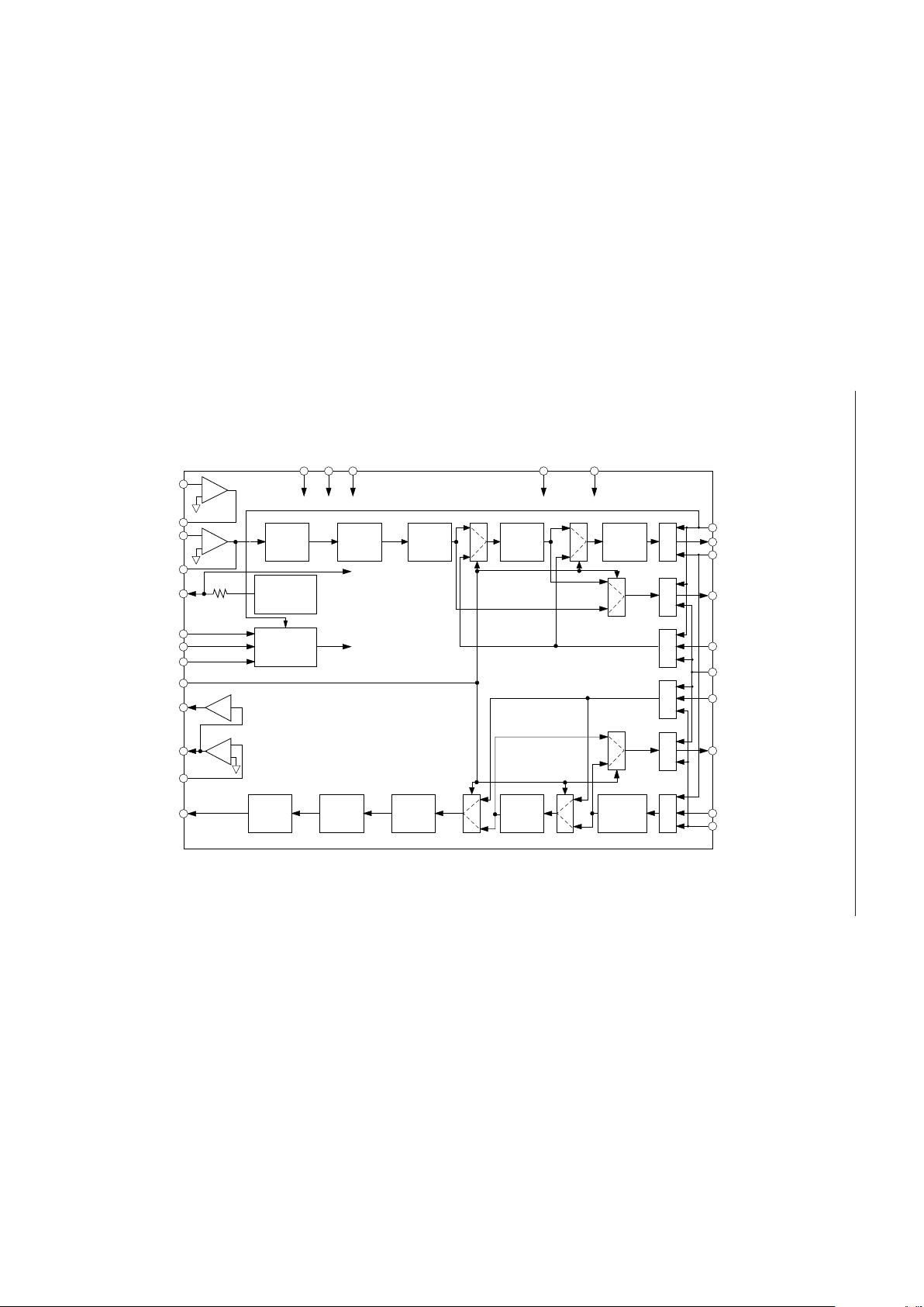
BLOCK DIAGRAM
AIN2
GSX2
XSYNC
IS
AIN1
GSX1
AOUT–
ADPCM
CODER
1
0
V
DD
BCLKA
0
1
PCMSO
PCMSI
PCMRI
PCMRO
IR
RSYNC
0
1
ADPCM
DECODER
1
0
BCLKB
AG DG X1 X2
PWI
V
REF
SG
CLOCK/
TIMING
MCK
LPS
RES
PDN
AOUT+
–
+
–1
VFRO
–
+
–
+
P
/
S
P
/
S
S
/
P
S
/
P
P
/
S
S
/
P
0
1
RCLPF
A/D
Conv.
BPF
EXPANDER
1
0
RCLPF
D/A
Conv.
LPF
COMPANDER
Page 3
FEDL7540-03
¡ Semiconductor
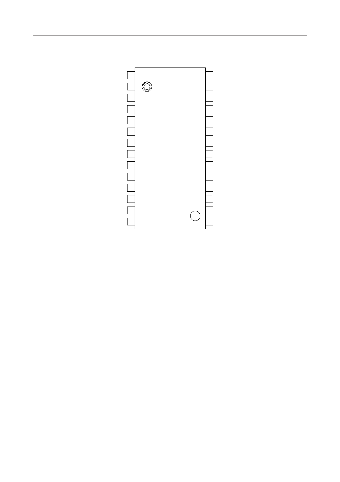
PIN CONFIGURATION (TOP VIEW)
1
RES
IR
IS
LPS
DG
AG
SG
2
3
4
5
6
7
8
9
10
11
PCMRI
PCMRO
PCMSI
PCMSO
28
27
26
25
24
23
22
21
20
19
18
BCLKB
BCLKA
XSYNC
RSYNC
MCK
X2
X1
PDN
V
DD
AOUT+
AOUT–
MSM7540/7560
12
AIN1
13
GSX1
14 15
AIN2 GSX2
17
16
PWI
VFRO
28-Pin Plastic SOP
3/16
Page 4
FEDL7540-03
(
)
¡ Semiconductor
MSM7540/7560
PIN AND FUNCTIONAL DESCRIPTIONS
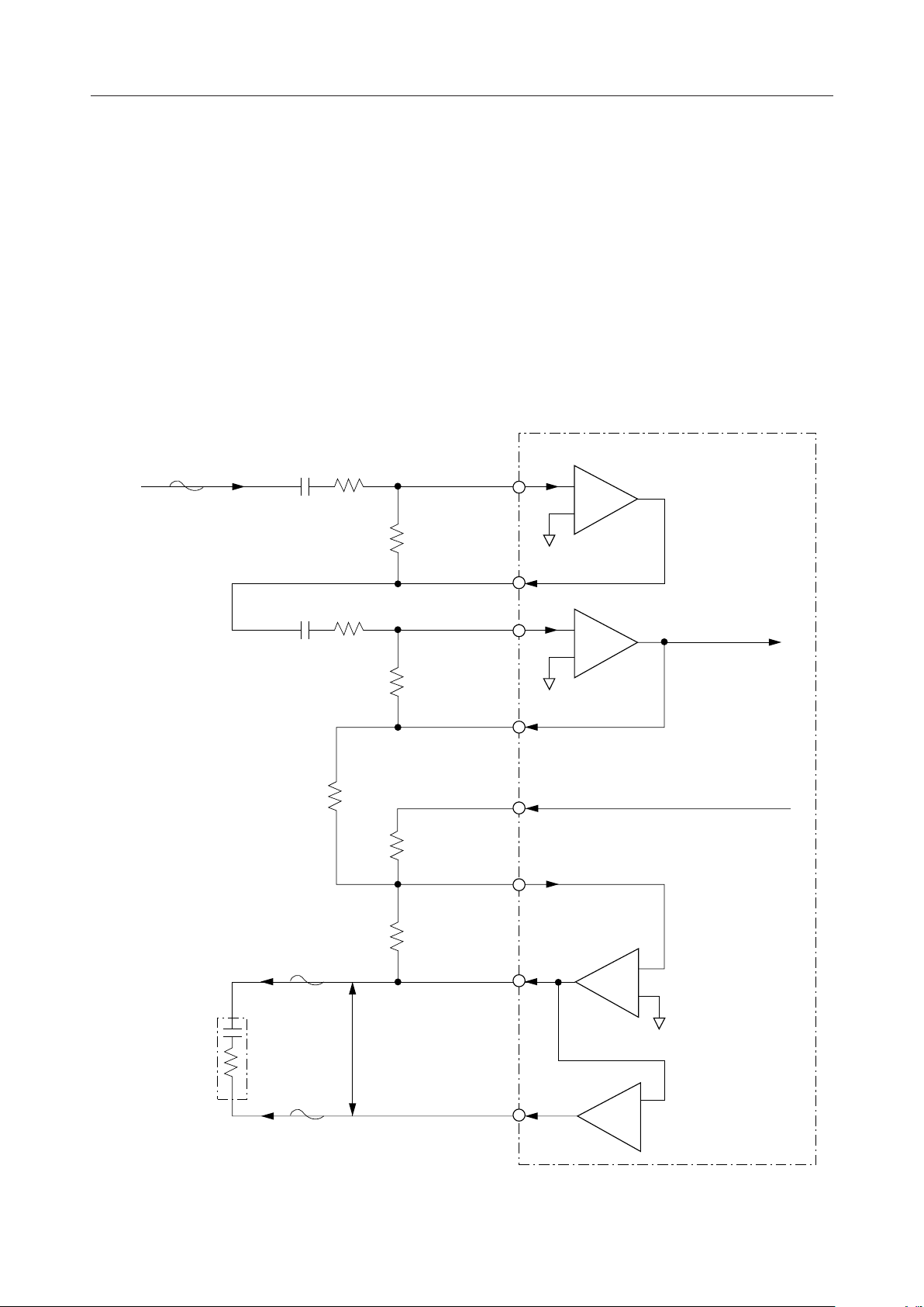
AIN1, AIN2, GSX1, GSX2
Transmit analog inputs and the output for transmit gain adjustment.
AIN1 (AIN2) connects to the inverting input of the internal transmit amplifier. GSX1 (GSX2)
connects to the internal transmit amplifier output. Refer to Fig. 1 for gain adjustment.
VFRO, AOUT+, AOUT–, PWI
Receive analog output and the output for receive gain adjustment.
VFRO is the receive filter output. AOUT+ and AOUT– are differential analog signal outputs
which can directly drive ZL = 350 W + 120 nF. Refer to Fig. 1 for gain adjustment.
Analog Input
C1
R1
AIN1
–
+
R2
Transmit Gain:
= (R2/R1) ¥ (R4/R3)
Receive Gain:
= (R6/R5)
C2
R3
RS*
R4
R5
R6
GSX1
AIN2
GSX2
VFRO
PWI
AOUT–
–
+
to ENCODER
from DECODER
–
+
V
+ 350 W
Analog OutputZL=120 nF
0
* : Side Tone Pass
Figure 1 Analog Input/Output Interface
–1
AOUT+
Gain = R6/RS
4/16
Page 5

FEDL7540-03
¡ Semiconductor
MSM7540/7560
SG
Analog signal ground voltage output.
The output voltage of this pin is approximately 2.4 V. Put bypass capacitors between this pin
and the AG pin. During power-down this output voltage is 0 V. The external SG voltage, if
necessary, should be used via a buffer.
AG
Analog ground.
DG
Digital ground.
This ground is separated internally from the analog signal ground pin (AG). The DG pin must
be kept as close as possible to AG on the PCB.
V
DD
+5 V power supply.
LPS
PCM coding law selection.
MSM7540 only ; if this pin goes to a "0" level, PCMSO, PCMSI, PCMRO, and PCMRI become the
A-law character signal, and if these pins goes to a "1" level, the signal becomes a linear value
character signal (2's complement).
MSM7560 only ; if this pin goes to a "0" level, PCMSO, PCMSI, PCMRO, and PCMRI become the
m-law character signal, and if these pins goes to a "1" level, the signal becomes a linear value
character signal (2's complement).
PDN
Power down control input.
If this pin is "0", this device is in the power-down state.
Normally, this pin is set to "1".
RES
Optional reset input specified by ITU-T Recommendation G. 721.
If this pin is "0", the device is in the reset state. The reset width (during "L") should be 125ms or
more.
MCK
Master clock input.
The frequency must be 10.368 MHz. The master clock signal may be asynchronous to BCLKA,
BCLKB, XSYNC, and RSYNC.
PCMSO
Transmit PCM data output.
PCM is output from MSB in synchronization with the rising edge of BCLKB and XSYNC.
5/16
Page 6

FEDL7540-03
¡ Semiconductor
PCMSI
Transmit PCM data input.
This signal is converted to the transmit ADPCM data. PCM is shifted in synchronization with
the falling edge of BCLKB. Normally, this pin is connected to PCMSO.
PCMRO
Receive PCM data output.
PCM is the output signal after ADPCM decoder processing. This signal is output serially from
MSB in synchronization with the rising edge of BCLKB and RSYNC.
PCMRI
Receive PCM data input.
PCM is shifted on the falling edge of the BCLKB and input from MSB. Normally, this pin is
connected to PCMRO.
IS
Transmit ADPCM signal output.
After having encoded PCM with ADPCM, this signal is output from MSB in synchronization
with the rising edge of BCLKA and XSYNC . This pin is an open drain output and remains in a
high impedance state during power-down. IS requires a pull-up resistor.
MSM7540/7560
IR
Receive ADPCM signal input.
The ADPCM signal is shifted in series and synchronization with the falling edge of BCLKA and
RSYNC, starting with MSB.
BCLKB
Shift clock input for the PCM data (PCMSO, PCMSI, PCMRO, PCMRI).
The frequency is set in the 64 kHz to 2048 kHz range.
XSYNC
8 kHz synchronous signal input for transmit PCM and ADPCM data.
Synchronize this signal with BCLKA and BCLKB signal. XSYNC is used to indicate the MSB of
the serial PCM and ADPCM data stream.
Be sure to input the XSYNC signal because it is also used as the input of the timing generator.
RSYNC
8 kHz synchronous signal input for receive PCM and ADPCM data.
Synchronize this signal with BCLKA and BCLKB signal. RSYNC is used to indicate the MSB of
the serial PCM and ADPCM data stream.
BCLKA
Shift clock input for the ADPCM data (IS, IR).
The frequency is set in the range of 32 kHz to 2048 kHz.
6/16
Page 7

FEDL7540-03
¡ Semiconductor
MSM7540/7560
X1, X2
Crystal oscillator (10.368 MHz) connection.
Connect X2, the clock output pin, directly to the MCK pin.
When using a conventional external clock of 10.368 MHz, X1 should be connected to the ground,
leave X2 open, and provide the external clock through the MCK pin.
<Using a self-oscilation circuit>
MSM7540/60
X1
10.368 MHz
X2
MCK
<Using an external clock>
MSM7540/60
MCK
X1
10.368 MHz
X2
7/16
Page 8

FEDL7540-03
¡ Semiconductor
ABSOLUTE MAXIMUM RATINGS
Parameter
Power Supply Voltage
Analog Input Voltage
Digital Input Voltage
Storage Temperature
Symbol
V
DD
V
AIN
V
DIN
T
STG
Condition
—
—
—
—
RECOMMENDED OPERATING CONDITIONS
Parameter
Power Supply Voltage
Operating Temperature
Input High Voltage
Input Low Voltage
Master Clock Frequency
Bit Clock Freqency
Synchronous Signal Frequency
Clock Duty Ratio
Digital Input Rise Time
Digital Input Fall Time
Transmit Sync Signal Setting Time
Receive Sync Signal Setting Time
Synchronous Signal Width
PCM, ADPCM Set-up Time
PCM, ADPCM Hold Time
Digital Output Load
Bypass Capacitor for SG
Symbol
V
DD
Ta
V
IH
V
IL
f
MCK
f
BCKA
f
BCKB
f
SYMC
D
C
t
Ir
t
If
t
XS
t
XS
t
RS
t
SR
t
WS
t
DS
t
DH
R
DL
C
DL
C
SG
Condition Min. Typ. Max. Unit
Voltage must be fixed 4.5 — 5.5 V
— –25 +25 +70 °C
MCK, XSYNC, RSYNC, PCMRI,
PCMSI, BCLKA, BCLKB, IR,
LPS, PDN, RES
MCK, XSYNC, RSYNC, PCMRI,
PCMSI, BCLKA, BCLKB, IR,
LPS, PDN, RES
MCK –
BCLKA 32 — 2048 kHz
BCLKB 64 — 2048 kHz
XSYNC, RSYNC — 8.0 — kHz
MCK, BCLKA, BCLKB 30 50 70
MCK, XSYNC, RSYNC, PCMRI,
PCMSI, BCLKA, BCLKB, IR,
LPS, PDN, RES
MCK, XSYNC, RSYNC, PCMRI,
PCMSI, BCLKA, BCLKB, IR,
LPS, PDN, RES
BCLKA, BCLKB to XSYNC 100 — — ns
XSYNC to BCLKA, BCLKB 100 — — ns
BCLKA, BCLKB to RSYNC 100 — — ns
RSYNC to BCLKA, BCLKB 100 — — ns
XSYNC, RSYNC 1 BCLK — 100 ms
— 100 — — ns
— 100 — — ns
IS (Pull-up Resistor) 500 — — W
IS, PCMSO, PCMRO
SG´GND
MSM7540/7560
DD
Unit
V
V
V
°C
V
MHz
%
Rating
–0.3 to +7
–0.3 to V
–0.3 to V
DD
DD
+ 0.3
+ 0.3
–55 to +150
2.2 — V
0 — 0.6 V
0.01%
10.368 +
0.01%
——50ns
——50ns
— — 100 pF
— 10 + 0.1 — mF
8/16
Page 9

FEDL7540-03
¡ Semiconductor
ELECTRICAL CHARACTERISTICS
DC and Digital Interface Characteristics
Parameter
Power Supply Current
Input High Voltage
Input Low Voltage
Input Leakage Current
Output Low Voltage
Output Leakage Current
Input Capacitance
Symbol
I
DD1
I
DD2
V
IH
V
IL
I
IH
I
IL
V
OL
I
O
C
IN
Operating Mode,
(When no signal, and
Power Down Mode
(When
VI = V
DD
VI = 0 V
1 LSTTL, Pull-up: 500 W
IS
MSM7540/7560
4.5 V to 5.5 V, Ta = –25°C to +70°C)
(V
DD =
Condition
= 5.0 V)
V
DD
= 5.0 V)
V
DD
—
—
— —5—pF
Min.
—
—
2.2
0.0
—
—
0.0
—
Typ.
12
0.2
—
—
—
—
0.2
—
Max.
24
0.5
V
DD
0.6
2.0
0.5
0.4
10
Unit
mA
mA
V
V
mA
mA
V
mA
Transmit Analog Interface Characteristics
Parameter
Input Resistance
Output Load Resistance
Output Load Capacitance
Output Amplitude
Input Offset Voltage
SG Output Voltage
SG Output Impedance
SG Rise Time T
Symbol
R
INX
R
LGX
C
LGX
V
OGX
V
OFGX
V
SG
R
SG
SG
Condition
AIN1, AIN2
GSX1, GSX2
GSX1, GSX2
GSX1, GSX2, R
= 50 kW
L
Pre–OPAMPs
—
—
SG´GND 10 mF + 0.1 mF
(Rise time to 90% of max. level)
Min.
* –3 dBm (600 W) = 0 dBm0, + 3.14 dBm0 = 2.226 VPP (MSM7540)
–3 dBm (600 W) = 0 dBm0, + 3.17 dBm0 = 2.226 VPP (MSM7560)
10
50
—
—
–20
—
—
Typ.
—
—
—
—
—
2.4
40
Max.
—
—
100
*2.226
+20
—
80
Unit
MW
V
— 700 — ms
kW
pF
PP
mV
V
kW
9/16
Page 10

FEDL7540-03
¡ Semiconductor
Receive Analog Interface Characteristics
Parameter
Input Resistance
Output Load Resistance
Output Capacitance
Output Voltage Level
Offset Voltage
Open Loop Gain
Symbol
R
INPW
R
LVF
R
LAO
C
LVF
C
LAO
V
OVF
V
OAO
V
OFVF
V
OFAO
G
DB
PWI
VFRO
AOUT+, AOUT–
VFRO
AOUT+, AOUT–
VFRO
AOUT+,
AOUT–
VFRO
AOUT+, AOUT– (GAIN = 0 dB),
Power amp only
Power amp (0.3 to 3.4 kHz,
ZL = 350 W + 120 nF)(See Fig.1)
Condition
RL = 50 kW
RL = 1.2 kW
ZL = 350 W
+ 120 nF(See Fig.1)
MSM7540/7560
Min.
10
50
1.2
—
—
—
—
—— V
–100
–20
40——dB
Typ.
—
—
—
—
—
—
—
—
—
Max.
—
—
—
100
100
*2.226
*2.226
*2.226
+100
+20
Unit
MW
kW
kW
pF
pF
V
PP
V
PP
PP
mV
mV
* –3 dBm (600 W) = 0 dBm0, + 3.14 dBm0 = 2.226 VPP (MSM7540)
–3 dBm (600 W) = 0 dBm0, + 3.17 dBm0 = 2.226 VPP (MSM7560)
10/16
Page 11

FEDL7540-03
¡ Semiconductor
AC Chracteristics
Parameter
Transmit Frequency
Response
Receive Frequency
Response
Transmit Signal
to Distortion Ratio
Receive Signal
to Distortion Ratio
Transmit Gain
Tracking
Receive Gain
Tracking
MSM7540/7560
4.5 V to 5.5 V, Ta = –25°C to +70°C)
(V
DD =
Condition
Symbol
L
T1
OSS
L
T2
OSS
L
T3
OSS
L
T4
OSS
L
T5
OSS
L
T6
OSS
L
R1
OSS
R2
L
OSS
R3
L
OSS
R4
L
OSS
R5
L
OSS
Freq.
0 to 60
300 to 3000 –0.15 — +0.20 dB
1020 Reference dB
3300 –0.15 — +0.80 dB
3400 0 — 0.80 dB
3968.75 14 — — dB
0 to 3000 –0.15 — +0.20 dB
1020 Reference dB
3300 –0.15 — +0.80 dB0
3400 0 — 0.80 dB
3968.75 14 — — dB
SD T1 35 —3
SD T2 35 —0
SD T3 35 —–30
1020
SD T4
SD T5 23 —–45
SD R1 —3
SD R2 —0
SD R3 —–30
1020
SD R4
SD R5 —–45
GT T1 –0.2 +0.2
GT T2 Reference
GT T3 1020 –0.2 +0.2–40
GT T4 –0.5 +0.5
GT T5 –1.2 +1.2
GT R1 –0.2 +0.2
GT R2 Reference
GT R3 1020 –0.2 +0.2
GT R4 –0.5 +0.5
GT R5 –1.2 +1.2
Level
(dBm0)(Hz)
–10
–50
–55
–10
–40
–50
–55
Others
25
Min.
0
—
Typ.
—
Max.—Unit
—
—
—
(*1)
28 —–40
—
—
—
35
35
(*1)
35
28
23
3
—
—
—
—
—
—
—
—
—
—
3
—
—
—
—
—
dB
dB
dB
dB
dB
dB
dB
dB
dB
—–40
dB
dB
dB
dB
dB
dB
dB
dB
dB
dB
dB
dB
*1 Use the P-message weighted filter
11/16
Page 12

FEDL7540-03
¡ Semiconductor
AC Characteristics (Continued)
Parameter
Idle Channel Noise
Absolute Signal
Amplitude
Power Supply Noise
Rejection Ratio
Digital Output
Delay Time
Symbol
N
IDLT
N
IDLR
A
VT
A
VR
P
SRRT
P
SRRR
t
SDX
t
SDR
t
, t
XD1
RD1
, t
t
XD2
RD2
t
, t
XD3
RD3
Noise Freq.
: 0 to 50 kHz
MSM7540/7560
(V
4.5 V to 5.5 V, Ta = –25°C to +70°C)
DD =
Condition
Freq.
———
——
1020
—
Level Min. Typ. Max. Unit
(dBm0)(Hz)
Others
–69
AIN = SG
(*1)
(–72)
—
(*1)
—
(*2)
–72
(–75)
0.548
GSX2
0.488
0.615
(*3)
0
0.548
VFRO
0.488
0.615
(*3)
Noise Level
30——dB
—
: 50 mV
PP
30——dB
50 — 200
50 — 200
1 LSTTL + 100 pF,
—
50 — 200
Pull-up: 500 W
50 — 200
50 — 200
dBm0p
(dBmp)
Vrms
Vrms
ns
ns
ns
ns
ns
*1 Use the P-message weighted filter
*2 PCMRI input code "11010101"(MSM7540)
"11111111"(MSM7560)
*3 0.548 Vrms = 0 dBm0= –3 dBm
Note: All ADPCM coder and decoder characteristics comply with ITU-T Recommendation
G.721.
12/16
Page 13

FEDL7540-03
(
)
¡ Semiconductor
TIMING DIAGRAM
Transmit Side PCM/ADPCM Data Interface
BCLKB
XSYNC
PCMSO
PCMSO
(during linear)
BCLKA
XSYNC
IS
012345678910
tsx
txs
txd1 txd2
tsdx
012345678910
txs
txd1 txd2
tsdx
tws
MSB LSB
MSB
tsx
txd3
MSB LSB
txd3
MSM7540/7560
11 12 13
14
txd3
LSB
Receive Side PCM/ADPCM Data Interface
BCLKA
RSYNC
IR
BCLKB
RSYNC
PCMRO
PCMRO
during linear
012345678910111213
tsr
trs
MSB LSB
012345678910
tsr
trs
tsdx
tws
tds
trd1
MSB LSB
MSB
tdh
trd2
Note: Linear format
A code of an input/output level is determined by the 14-bit 2'compliment.
Refer to the table below for code format.
Input/Output level
+Full-scall
0
–Full-scall
14
txd3
txd3
trd3
LSB
MSB to LSB
01111111111111
00000000000000
10000000000000
13/16
Page 14

FEDL7540-03
¡ Semiconductor
APPLICATION CIRCUIT
V
DD
Receive
PCM Output
Receive ADPCM Input
Transmit ADPCM Output
Transmit
PCM Output
Transmit Analog Input
MSM7540/7560GS
1
RES
2
PCMRI
3
PCMRO
4
IR
5
IS
6
PCMSI
7
PCMSO
8
LPS
9
DG
10
AG
11
SG AOUT–
12
AIN1 PWI
13
GSX1 VFRO
14
AIN2 GSX2
BCLKB
BCLKA
XSYNC
RSYNC
MCK
X2
X1
PDN
V
DD
AOUT+
28
27
26
25
24
23
22
21
20
19
18
17
16
15
V
DD
10.368 MHz
MSM7540/7560
ADPCM Algorithm
Reset Input
Shift Clock Input for
PCM, ADPCM Data
(64 kHz to 2048 kHz)
8 kHz Sync Signal Input
Power Down Input
Receive Analog Output
(Push-Pull)
14/16
Page 15

FEDL7540-03
¡ Semiconductor
PACKAGE DIMENSIONS
SOP28-P-430-1.27-K
Mirror finish
MSM7540/7560
(Unit : mm)
Package material
Lead frame material
Pin treatment
Solder plate thickness
Package weight (g)
Epoxy resin
42 alloy
Solder plating
5 mm or more
0.75 TYP.
Notes for Mounting the Surface Mount Type Package
The SOP, QFP, TSOP, SOJ, QFJ (PLCC), SHP and BGA are surface mount type packages, which
are very susceptible to heat in reflow mounting and humidity absorbed in storage.
Therefore, before you perform reflow mounting, contact Oki’s responsible sales person for the
product name, package name, pin number, package code and desired mounting conditions
(reflow method, temperature and times).
15/16
Page 16

FEDL7540-03
¡ Semiconductor
MSM7540/7560
NOTICE
1. The information contained herein can change without notice owing to product and/or
technical improvements. Before using the product, please make sure that the information
being referred to is up-to-date.
2. The outline of action and examples for application circuits described herein have been
chosen as an explanation for the standard action and performance of the product. When
planning to use the product, please ensure that the external conditions are reflected in the
actual circuit, assembly, and program designs.
3. When designing your product, please use our product below the specified maximum
ratings and within the specified operating ranges including, but not limited to, operating
voltage, power dissipation, and operating temperature.
4. Oki assumes no responsibility or liability whatsoever for any failure or unusual or
unexpected operation resulting from misuse, neglect, improper installation, repair, alteration
or accident, improper handling, or unusual physical or electrical stress including, but not
limited to, exposure to parameters beyond the specified maximum ratings or operation
outside the specified operating range.
5. Neither indemnity against nor license of a third party’s industrial and intellectual property
right, etc. is granted by us in connection with the use of the product and/or the information
and drawings contained herein. No responsibility is assumed by us for any infringement
of a third party’s right which may result from the use thereof.
6. The products listed in this document are intended for use in general electronics equipment
for commercial applications (e.g., office automation, communication equipment,
measurement equipment, consumer electronics, etc.). These products are not authorized
for use in any system or application that requires special or enhanced quality and reliability
characteristics nor in any system or application where the failure of such system or
application may result in the loss or damage of property, or death or injury to humans.
Such applications include, but are not limited to, traffic and automotive equipment, safety
devices, aerospace equipment, nuclear power control, medical equipment, and life-support
systems.
7. Certain products in this document may need government approval before they can be
exported to particular countries. The purchaser assumes the responsibility of determining
the legality of export of these products and will take appropriate and necessary steps at their
own expense for these.
8. No part of the contents contained herein may be reprinted or reproduced without our prior
permission.
9. MS-DOS is a registered trademark of Microsoft Corporation.
Copyright 1999 Oki Electric Industry Co., Ltd.
Printed in Japan
16/16
 Loading...