

Page 1

E2A0014-16-X0
SUNSTAR电子元器件 http://www.sunstare.com/ TEL: 0755-83376282 FAX:0755-83376182 E-MAIL:szss20@163.com
SUNSTAR电子元器件 http://www.sunstare.com/ TEL: 0755-83778810 FAX:0755-83376182 E-MAIL:szss20@163.com
Semiconductor MSM7512B
¡ Semiconductor
This version: Jan. 1998
Previous version: Nov. 1996
MSM7512B
1200 bps Half Duplex FSK Modem – ITU-T V.23
GENERAL DESCRIPTION
The MSM7512B is useful for the ITU-T V.23 modem, for examples, low cost built-in modems,
telecontrol systems, home security systems, etc.
The family version, MSM7510 for ITU-T V.21, will be available following this device.
Oki has been mass-producing and delivering the MSM6926 and 6927 for a long time, but these
devices need two power supplies, +5 V for digital and +12 V for analog.
New generation devices, MSM7510/7512B, work with single rail +3 V to +5 V and low power
consumption.
FEATURES
• Conforms to ITU-T V.23, 1200 bps Half Duplex
• Conforms to ITU-T V.23, 75 bps transmitter
• Single Power Supply: +3 V to +5 V
• Low Power Consumption
Operating Mode: 25 mW Typ.
Power Down Mode: 0.1 mW Max.
• Line Hybrid Circuit on Chip
• Line Direct Drive Capability of Analog Output
• 3.579545 MHz Crystal Oscillator
• Digital Interface: TTL
• Package options:
16-pin plastic DIP (DIP16-P-300–2.54) (Product name: MSM7512BRS)
24-pin plastic SOP (SOP24-P-430-1.27–K) (Product name: MSM7512BGS-K)
1/12
Page 2
SUNSTAR电子元器件 http://www.sunstare.com/ TEL: 0755-83376282 FAX:0755-83376182 E-MAIL:szss20@163.com
SUNSTAR电子元器件 http://www.sunstare.com/ TEL: 0755-83778810 FAX:0755-83376182 E-MAIL:szss20@163.com
Semiconductor MSM7512B
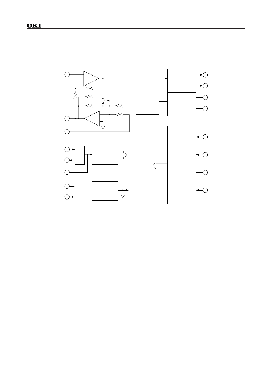
BLOCK DIAGRAM
AI
(2)
AO
(3)
EAI
(4)
X1
(6)
X2
(7)
CLK
(8)
V
DD
(1)
GND
(5)
*R1
OSC
+
–
*R1
*R2
*R2
–
+
CLK GEN.
SG GEN.
AOG
*R3
*R2
* R1 to R3 ≥ 50 kW
FSK & ANS
Bandpass
Filter
Demodulator
Modulator
CONT.
RD
(9)
CD
(10)
XD
(11)
RS
(12)
TEST
(13)
MOD1
(14)
MOD2
(15)
AOG
(16)
( ) : for MSM7512BRS
2/12
Page 3
SUNSTAR电子元器件 http://www.sunstare.com/ TEL: 0755-83376282 FAX:0755-83376182 E-MAIL:szss20@163.com
SUNSTAR电子元器件 http://www.sunstare.com/ TEL: 0755-83778810 FAX:0755-83376182 E-MAIL:szss20@163.com
Semiconductor MSM7512B
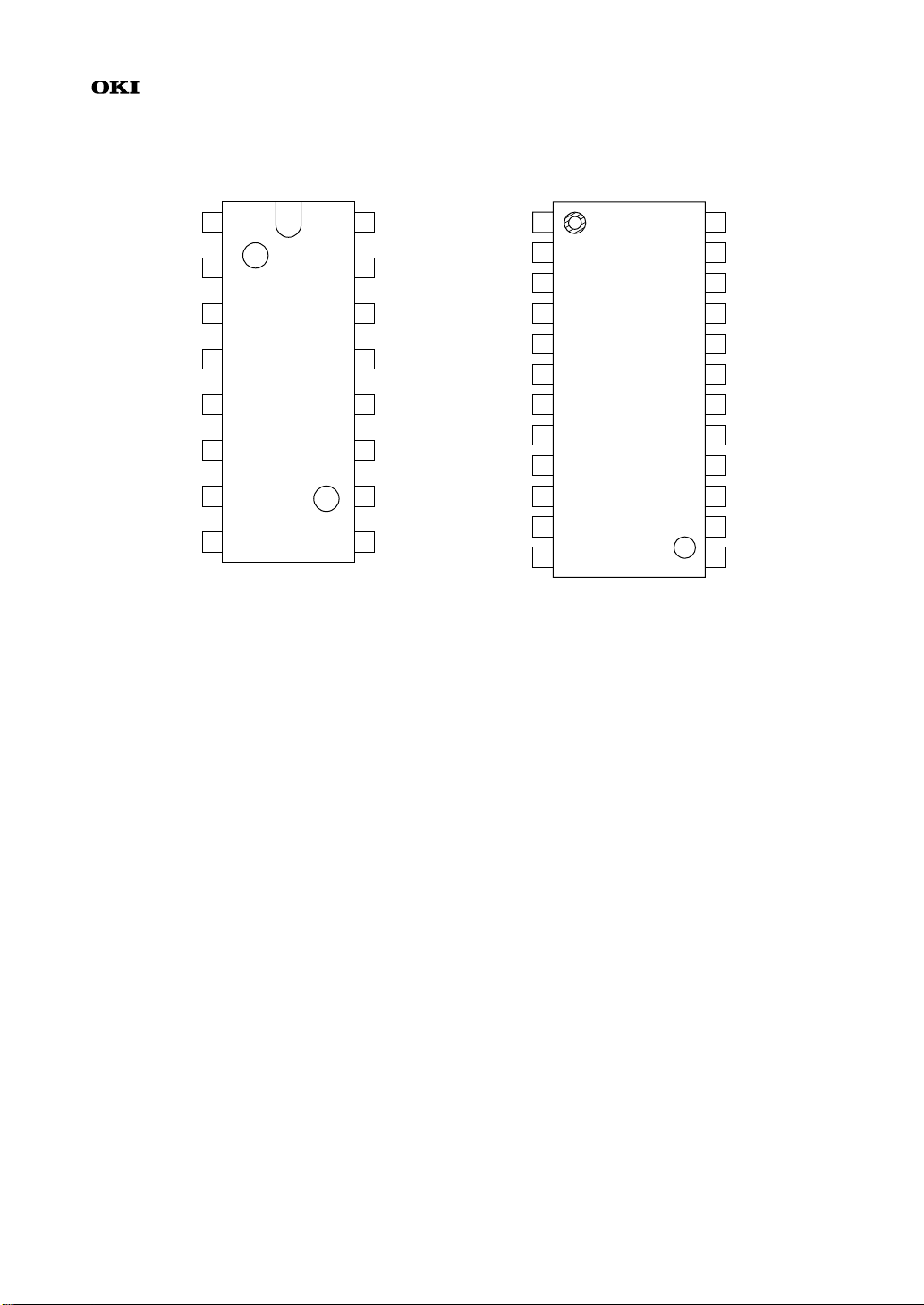
PIN CONFIGURATION (TOP VIEW)
1
DD
2
AI
3
AO
4
EAI
5
GND
6
X1
7
X2
8 9
CLK
16-Pin Plastic DIP
16V
15
14
13
12
11
10
AOG
MOD2
MOD1
TEST
RS
XD
CD
RD
1
DD
2
NC
3
AI
4
NC
5
AO
6
EAI
7
GND
8
X1
9
NC
10
X2
11
NC
12 13
CLK
24-Pin Plastic SOP
NC : No connect pin
24V
23
22
21
20
19
18
17
16
15
14
AOG
NC
MOD2
NC
MOD1
TEST
RS
XD
NC
CD
NC
RD
3/12
Page 4
SUNSTAR电子元器件 http://www.sunstare.com/ TEL: 0755-83376282 FAX:0755-83376182 E-MAIL:szss20@163.com
SUNSTAR电子元器件 http://www.sunstare.com/ TEL: 0755-83778810 FAX:0755-83376182 E-MAIL:szss20@163.com
Semiconductor MSM7512B
PIN DESCRIPTION
No.
RS GS-VK
11 VDD— +3 V to +5 V Power Supply
2 3 AI I Analog receive signal input.
3 5 AO O Analog transmit signal output.
External analog signal input.
4 6 EAI I
5 7 GND — Ground, 0 V.
6 8 X1 I
710 X2 O
8 12 CLK O 3.579545 MHz clock signal output.
913 RD O
10 15 CD O
11 17 XD I*
12 18 RS I*
13 19 TEST I*
14 20 MOD1 I* Operation mode select.
15 22 MOD2 I*
16 24 AOG I*
The signal applied to this pin is transmitted from AO via transmit output
amplifier. When not using this pin, it should be left open.
3.579545 MHz crystal resonator should be connected to X1 and X2.
When applying external clock 3.579545 MHz to the device, it should be
applied to X2 (not X1) via an AC-coupling capacitor of 100 pF and X1
has to be opened.
Modem receive serial data output.
Digital "1" and "0" correspond to "Mark" and "Space", respectively. When
CD (Carrier Detect) is off, RD is held at "Mark" state.
FSK Receive signal and answer tone detect.
Digital "0" and "1" represent "Detect" and "Non-detect", respectively.
Modem transmit serial data input.
Digital "1" and "0" correspond to "Mark" and "Space", respectively.
FSK signal and answer tone transmit enable.
When digital "0" is applied to RS, transmitting becomes enable.
Chip test input.
TEST should be open or digital "1".
Refer to Table 1.
Analog transmit signal amplitude select.
Digital "1" Æ –10 dBm Typ. at AO
Digital "0" Æ –4 dBm Typ. at AO
DescriptionName I/O
Note : I* : Internally pulled-up input pin.
4/12
Page 5

SUNSTAR电子元器件 http://www.sunstare.com/ TEL: 0755-83376282 FAX:0755-83376182 E-MAIL:szss20@163.com
SUNSTAR电子元器件 http://www.sunstare.com/ TEL: 0755-83778810 FAX:0755-83376182 E-MAIL:szss20@163.com
Semiconductor MSM7512B
ABSOLUTE MAXIMUM RATINGS
Symbol Condition Rating UnitParameter
Power Supply Voltage V
Input Voltage V
Storage Temperature T
DD
IN
STG
Ta = 25°C,
With respect to GND
–0.3 to +7 V
–0.3 to VDD + 0.3 V
–55 to +150 °C—
RECOMMENDED OPERATING CONDITIONS
Parameter
Power Supply Voltage V+5.5—+2.7—V
Operating Temperature °C+85—–40—T
Input Clock Frequency %+0.1—–0.1To 3.579545 MHzf
VDD Bypass Capacitor mF——10V
DD
op
CLK
VDD
Oscillation Frequency MHz—3.579545———
Frequency Deviation ppm+100—–100+25°C ±5°C—
Temperature Characteristics ppm+50—–50–40°C to +85°C—
Crystal
Equivalent Series Resistance W50————
Load Capacitance pF—16———
ELECTRICAL CHARACTERISTICS
DC Characteristics
Symbol Condition Min. Typ. Max. UnitParameter
Power Supply Current
Digital Input Voltage
Digital Input Leakage Current
Digital Output Voltage
I
DD
I
SS
V
IL
V
IH
I
IL
I
IH
V
OL
V
OH
Operating Mode — 5.0 10.0 mA
Power Down Mode — 5.0 20.0 mA
I
– GNDC
DD
( VDD = +2.7 V to +5.5 V, Top = –40°C to +85°C)
— 0 — 0.8 V
— 2.2 — V
DD
VI = 0 V * –80 — 10 mA
VI = 5 V –10 — 10 mA
I
= 1.6 mA 0 0.2 0.4 V
OL
= –0.4 mA 2.4 — V
OH
DD
UnitMax.Typ.Min.ConditionSymbol
V
V
* Internally pulled-up pins
5/12
Page 6

SUNSTAR电子元器件 http://www.sunstare.com/ TEL: 0755-83376282 FAX:0755-83376182 E-MAIL:szss20@163.com
SUNSTAR电子元器件 http://www.sunstare.com/ TEL: 0755-83778810 FAX:0755-83376182 E-MAIL:szss20@163.com
Semiconductor MSM7512B
AC Characteristics
Modulator/analog output (AO) characteristics
(VDD = +2.7 V to +5.5 V, Top = –40°C to +85°C)
Symbol Condition Min. Typ. Max. UnitParameter
FSK Transmit
Signal Frequency
FSK Transmit Signal
Answer Tone amplitude
Analog External
Input Signal Gain
FSK Transmit
Signal Amplitude
Ratio
Out-of-band
Energy
Output Offset Voltage
Output Load Resistance
V
V
V
V
V
f
DM
f
f
BM
f
AO1
AO2
EA1
EA2
AOD
SPS
1200 bps Transmit Mode
DS
75 bps Transmit Mode
BS
P : In-band Signal
Energy
OFF
AO
V
O
VAO – V
(MARK) – VAO(SPACE) –2 0 2 dBV
V
AO
EAI
To V
DD
— 600 — — WR
XD = "1"
XD = "0"
XD = "1"
XD = "0"
AOG = "0"
AOG = "1"
AOG = "0"
AOG = "1"
4 kHz to 8 kHz
1296
2096
386
446
–6
–12
–2
–8
1300
2100
390
450
–4
–10
0
–6
——P–20
8 kHz to 12 kHz——
More than12 kHz — — P–60 dB
/2 –150 — +150 mVV
1304
2104HzHz
394
454HzHz
–2–8dBm
dBm
2
–4dBdB
P–40dBdB
* 0 dBm = 0.775 Vrms
6/12
Page 7

SUNSTAR电子元器件 http://www.sunstare.com/ TEL: 0755-83376282 FAX:0755-83376182 E-MAIL:szss20@163.com
SUNSTAR电子元器件 http://www.sunstare.com/ TEL: 0755-83778810 FAX:0755-83376182 E-MAIL:szss20@163.com
Semiconductor MSM7512B
Demodulator analog input (Al, EAI) characteristics
( VDD = +2.7 V to +5.5 V, Top = –40°C to +85°C)
Symbol Condition Min. Typ. Max. UnitParameter
Receive Signal
Amplitude
Receive Signal
Detect Amplitude (CD)
Hysteresis (CD)
CD Delay Time
CD Hold Time
Receive Data (RD)
Bias Distortion
Input Resistance
V
V
AI
ON
OFF
HYS
CDD
CDH
BS
AI
EAI
FSK Signal, (1:1) at AI
1200 bps, 1:1 Pattern –10 — 10 %D
FSK Signal, at AI — — –6 dBmV
VON Æ V
See Fig. 1
OFF Æ ON
OFF Æ OFF—–48
OFF
—2—dBV
—
—
51520mst
20 40 60 mst
AI — 10 — MWR
EAI 20 — — kWR
* 0 dBm = 0.775 Vrms
–42 dBm
dBm
—
AI
CD
t
CDD
t
CDH
Figure 1 Carrier Detect (CD) Timing
7/12
Page 8

SUNSTAR电子元器件 http://www.sunstare.com/ TEL: 0755-83376282 FAX:0755-83376182 E-MAIL:szss20@163.com
SUNSTAR电子元器件 http://www.sunstare.com/ TEL: 0755-83778810 FAX:0755-83376182 E-MAIL:szss20@163.com
Semiconductor MSM7512B
OPERATION MODE
Table 1 Operation Mode
MOD2 MOD1
00
01
10
11
AI
Phone
Line
AO
Receive Filter
SG V
Transmit Filter
Figure 2 FSK Transmit Mode
AI
Phone
Line
AO
Receive Filter
Transmit Filter
Mode
FSK Transmit Mode (Fig.2)
FSK Receive & 75 bps Transmit Mode (Fig.3)
Analog Loop Back Test Mode (Fig. 4)
Power Down Mode
Demodulator
Modulator
Demodulator
Modulator
DD
RD
DTE
XD
RD
DTE
XD
Figure 3 FSK Receive Mode
AI
Phone
Line
Receive Filter
Demodulator
AO
Transmit Filter
Modulator
SG
Figure 4 Analog Loop Back Test Mode
RD
DTE
XD
8/12
Page 9

SUNSTAR电子元器件 http://www.sunstare.com/ TEL: 0755-83376282 FAX:0755-83376182 E-MAIL:szss20@163.com
SUNSTAR电子元器件 http://www.sunstare.com/ TEL: 0755-83778810 FAX:0755-83376182 E-MAIL:szss20@163.com
Semiconductor MSM7512B
APPLICATION CIRCUIT
➀
MSM7512BRS
➁
Line
600 W :
Line
600 W
600 W :
2.2 mF
600 W
External Clock
3.58 MHz
600 W
2.2 mF
3.58 MHz
600 W
+
10 mF
100 pF
1
–
8
V
AI
AO
EAI
DD
AOG
MOD
MOD
TEST
GND
X1
X2
CLK RD
MSM7512BRS
1
V
DD
AI
AO
EAI
–
+
GND
10 mF
X1
X2
CLK RD
8
16
2
1
RS
XD
CD
9
To other circuit
AOG
MOD
2
MOD
1
TEST
RS
XD
CD
CONT.
16
CONT.
9
External Analog
2.2 mF
Transmit Signal
9/12
Page 10

SUNSTAR电子元器件 http://www.sunstare.com/ TEL: 0755-83376282 FAX:0755-83376182 E-MAIL:szss20@163.com
SUNSTAR电子元器件 http://www.sunstare.com/ TEL: 0755-83778810 FAX:0755-83376182 E-MAIL:szss20@163.com
Semiconductor MSM7512B
An Example of the External Adjustment for a transmitting Level and detecting Level
If you desire to change the transmitting level or detecting level, adjust the external circuit
by referring to the following circuit.
51 kW
VAOL
Line
51 kW
–
+
600 W
600 W
VAIL
Line transmitting level :
V
AOL
IC input level : VAI = V
R2
R1
–
+
R4
R3
–
+
= VAO ¥ (R2/R1)
¥ (R4/R3)
AIL
2.2 mF
2.2 mF
VAO
AO
51 kW
51 kW
AI
VAI
10/12
Page 11

SUNSTAR电子元器件 http://www.sunstare.com/ TEL: 0755-83376282 FAX:0755-83376182 E-MAIL:szss20@163.com
SUNSTAR电子元器件 http://www.sunstare.com/ TEL: 0755-83778810 FAX:0755-83376182 E-MAIL:szss20@163.com
Semiconductor MSM7512B
PACKAGE DIMENSIONS
DIP16-P-300-2.54
(Unit : mm)
Package material
Lead frame material
Pin treatment
Solder plate thickness
Package weight (g)
Epoxy resin
42 alloy
Solder plating
5 mm or more
0.99 TYP.
11/12
Page 12

SUNSTAR电子元器件 http://www.sunstare.com/ TEL: 0755-83376282 FAX:0755-83376182 E-MAIL:szss20@163.com
SUNSTAR电子元器件 http://www.sunstare.com/ TEL: 0755-83778810 FAX:0755-83376182 E-MAIL:szss20@163.com
Semiconductor MSM7512B
SOP24-P-430-1.27-K
Mirror finish
(Unit : mm)
Package material
Lead frame material
Pin treatment
Solder plate thickness
Package weight (g)
Epoxy resin
42 alloy
Solder plating
5 mm or more
0.58 TYP.
Notes for Mounting the Surface Mount Type Package
The SOP, QFP, TSOP, SOJ, QFJ (PLCC), SHP and BGA are surface mount type packages, which
are very susceptible to heat in reflow mounting and humidity absorbed in storage.
Therefore, before you perform reflow mounting, contact Oki’s responsible sales person for the
product name, package name, pin number, package code and desired mounting conditions
(reflow method, temperature and times).
12/12
Page 13

欢迎索取免费详细资料、设计选型指南和光盘、样品;产品繁多未能尽录,欢迎
SUNSTAR电子元器件 http://www.sunstare.com/ TEL: 0755-83376282 FAX:0755-83376182 E-MAIL:szss20@163.com
SUNSTAR电子元器件 http://www.sunstare.com/ TEL: 0755-83778810 FAX:0755-83376182 E-MAIL:szss20@163.com
来电查询。
中国传感器科技信息网:HTTP://WWW.SENSOR-IC.COM/
工控安防网:HTTP://WWW.PC-PS.NET/
消费电子专用电路网:HTTP://WWW.SUNSTARE.COM/
E-MAIL: xjr5@163.com szss20@163.com
MSN: suns8888@hotmail.com
QQ: 195847376
地址: 深圳市福田区福华路福庆街鸿图大厦 1602 室
电话:0755-83376549 83376489 83387030 83387016
传真:0755-83376182 83338339 邮编:518033 手机:(0)13902971329
深圳展销部: 深圳华强北路赛格电子市场 2583 号 TEL/FAX :
0755-83665529 25059422
北京分公司:北京海淀区知春路 132 号中发电子大厦 3097 号
TEL:010-81159046 82615020 13501189838 FAX:010-82613476
上海分公司:上海市北京东路 668 号上海賽格电子市场 2B35 号
TEL:021-28311762 56703037 13701955389 FAX:021-56703037
西安分公司:西安高新开发区 20 所(中国电子科技集团导航技术研究所)
西安劳动南路 88 号电子商城二楼 D23 号
TEL:029-81022619 13072977981 FAX:029-88789382
成都:TEL:(0)13717066236
技术支持:0755-83394033 13501568376
 Loading...