

Page 1

E2A0013-16-X1
Semiconductor MSM7510
¡ Semiconductor
This version: Jan. 1998
Previous version: Nov. 1996
MSM7510
300 bps Full Duplex FSK Modem – ITU-T V.21
GENERAL DESCRIPTION
The MSM7510 is useful for the ITU-T V.21 modem, for examples, low cost built-in modems,
telecontrol systems, home security systems, etc.
The family version, MSM7512B for ITU-T V.23, will be available following this device.
Oki has been mass-producing and delivering the MSM6926 and 6927 for a long time, but these
devices need two power supplies, +5 V for digital and +12 V for analog.
New generation devices, MSM7510/7512B, work with single rail +3 V to +5 V and low power
consumption.
FEATURES
• Conforms to ITU-T V.21, 300 bps Full Duplex
• ITU-T V.25 Answer Tone (2100 Hz) with Generator/Detector
• Single Power Supply : +3 V to +5 V
• Low Power Consumption
Operating Mode: 25 mW Typ.
Power Down Mode : 0.1 mW Max.
• Line Hybrid Circuit on Chip (direct drive capability of 600W)
• ALB (Analog–Loop back) with test mode.
• 3.579545 MHz Crystal Oscillator
• Digital Interface: TTL
• Package options:
16-pin plastic DIP (DIP16-P-300-2.45) (Product name: MSM7510RS)
24-pin plastic SOP (SOP24-P-430-1.27-K) (Product name: MSM7510GS-K)
1/12
Page 2
Semiconductor MSM7510
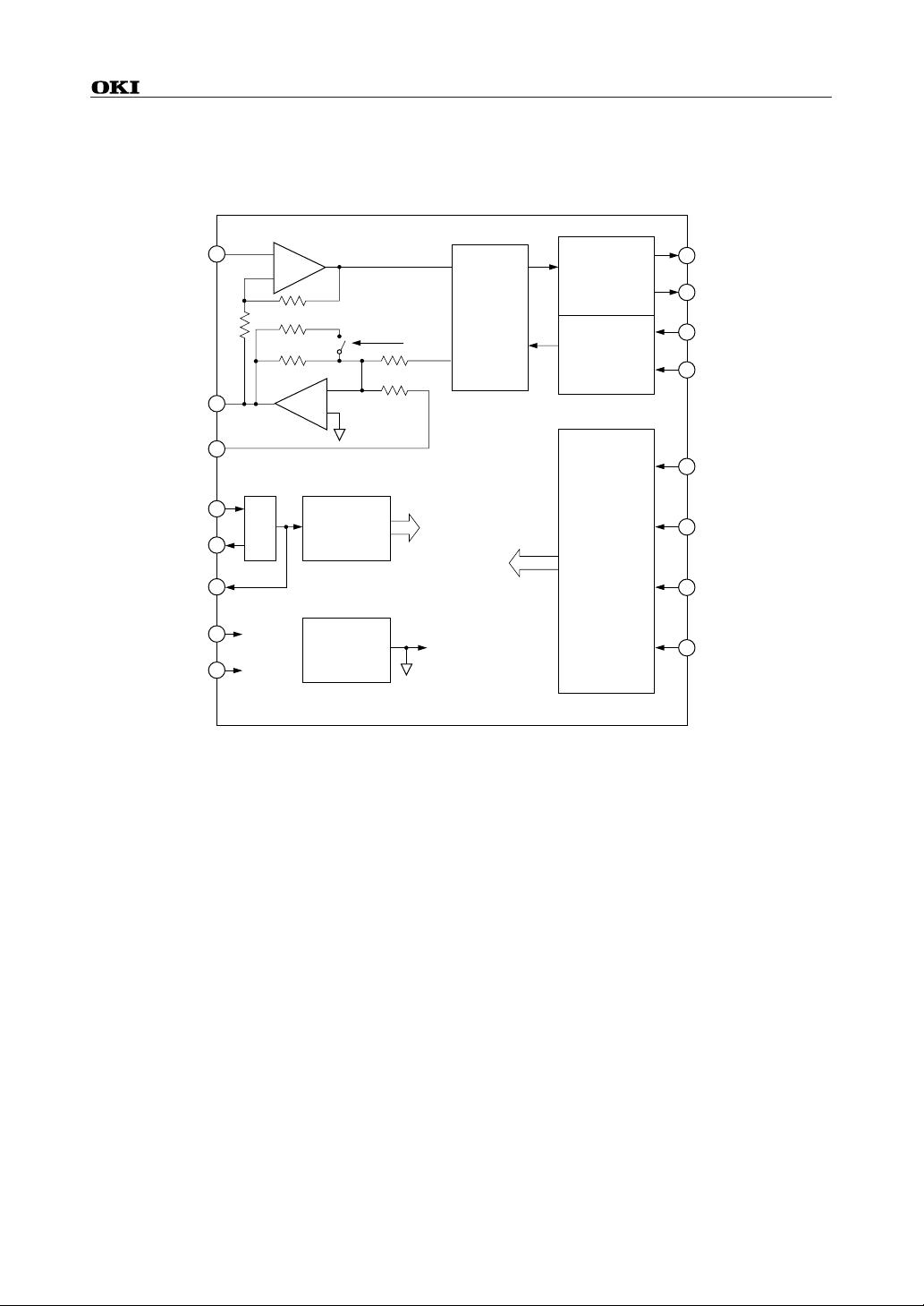
BLOCK DIAGRAM
AI
(2)
AO
(3)
EAI
(4)
X1
(6)
X2
(7)
CLK
(8)
V
DD
(1)
GND
(5)
*R1
OSC
+
–
*R1
*R2
*R2
–
+
CLK GEN.
SG GEN.
AOG
*R3
*R2
* R1 to R3 ≥ 50 kW
FSK & ANS
Bandpass
Filter
Demodulator
Modulator
CONT.
RD
(9)
CD
(10)
XD
(11)
RS
(12)
O/A
(13)
MOD1
(14)
MOD2
(15)
AOG
(16)
( ) : for MSM7510RS
2/12
Page 3
p
Semiconductor MSM7510
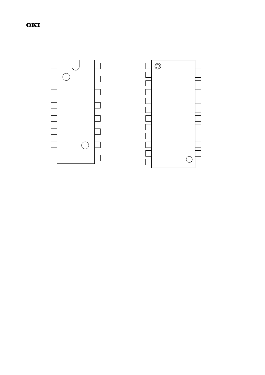
PIN CONFIGURATION (TOP VIEW)
1
V
DD
2
AI
3
AO
4
EAI
5
GND
6
X1
7
X2
8 9
CLK
16-Pin Plastic DIP
16
15
14
13
12
11
10
AOG
MOD2
MOD1
O/A
RS
XD
CD
RD
1
V
DD
2
NC
3
AI
4
NC
5
AO
6
EAI
7
GND
8
X1
9
NC
10
X2
11
NC
12 13
CLK
24-Pin Plastic SOP
NC: No connect
AOG
24
23
NC
MOD2
22
NC
21
20
MOD1
19
O/A
18
RS
17
XD
NC
16
CD
15
14
NC
RD
in
3/12
Page 4
Semiconductor MSM7510
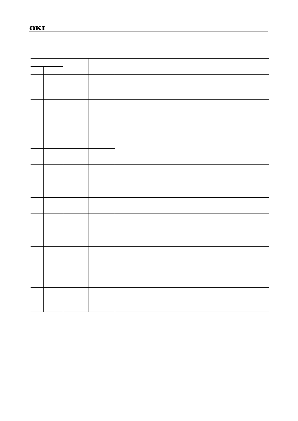
PIN DESCRIPTION
No.
RS GS-VK
11 VDD— +3 V to +5 V Power Supply
2 3 AI I Analog receive signal input.
3 5 AO O Analog transmit signal output.
External analog signal input.
4 6 EAI I
5 7 GND — Ground, 0 V.
6 8 X1 I
710 X2 O
8 12 CLK O 3.579545 MHz clock signal output.
913 RD O
10 15 CD O
11 17 XD I*
12 18 RS I*
13 19 O/A I*
14 20 MOD1 I* Operation mode select.
15 22 MOD2 I*
16 24 AOG I*
The signal applied to this pin is transmitted from AO via transmit output
amplifier. When not using this pin, it should be left opened.
3.579545 MHz crystal resonator should be connected to X1 and X2.
When applying external clock 3.579545 MHz to the device, it should be
applied to X2 (not X1) via an AC-coupling capacitor of 100 pF and X1
has to be opened.
Modem receive serial data output.
Digital "1" and "0" correspond to "Mark" and "Space", respectively. When
CD (Carrier Detect) is off, RD is held at "Mark" state.
FSK receive signal and answer tone detect.
Digital "0" and "1" represent "Detect" and "Non-detect", respectively.
Modem transmit serial data input.
Digital "1" and "0" correspond to "Mark" and "Space", respectively.
FSK signal and answer tone transmit enable.
When digital "0" is applied to RS, transmitting becomes enable.
Originate/Answer mode select.
Digital "1" Æ Originate mode
Digital "0" Æ Answer mode
Refer to Table 1.
Analog transmit signal amplitude select.
Digital "1" Æ –10 dBm Typ. at AO
Digital "0" Æ –4 dBm Typ. at AO
Note : I* : Internally pulled-up input pin.
DescriptionName I/O
4/12
Page 5

Semiconductor MSM7510
ABSOLUTE MAXIMUM RATINGS
Symbol Condition Rating UnitParameter
Power Supply Voltage V
Input Voltage V
Storage Temperature T
DD
IN
STG
Ta = 25°C,
With respect to GND
–0.3 to +7 V
–0.3 to VDD + 0.3 V
–55 to +150 °C—
RECOMMENDED OPERATING CONDITIONS
Parameter
Power Supply Voltage V+5.5—+2.7—V
DD
Operating Temperature °C+85—–40—Top
Input Clock Frequency %+0.1—–0.1To 3.579545 MHzf
VDD Bypass Capacitor mF——10V
CLK
VDD
Oscillation Frequency MHz—3.579545———
Frequency Deviation ppm+100—–100+25°C ±5°C—
Temperature Characteristics ppm+50—–50–40°C to +85°C—
Crystal
Equivalent Series Resistance W50————
Load Capacitance pF—16———
ELECTRICAL CHARACTERISTICS
DC Characteristics
Symbol Condition Min. Typ. Max. UnitParameter
Power Supply Current
Digital Input Voltage
Digital Input Leakage Current
Digital Output Voltage
I
DD
I
SS
V
IL
V
IH
I
IL
I
IH
V
OL
V
OH
Operating Mode — 5.0 10.0 mA
Power Down Mode — 5.0 20.0 mA
I
I
OH
UnitMax.Typ.Min.ConditionSymbol
– GNDC
DD
( VDD = +2.7 V to +5.5 V, Top = –40°C to +85°C)
— 0 — 0.8 V
— 2.2 — V
DD
VI = 0 V * –80 — 10 mA
VI = 5 V –10 — 10 mA
= 1.6 mA 0 0.2 0.4 V
OL
= –0.4 mA 2.4 — V
DD
V
V
* Internally pulled-up pins
5/12
Page 6

Semiconductor MSM7510
AC Characteristics
Modulator/analog output (AO) characteristics
(VDD = +2.7 V to +5.5 V, Top = –40°C to +85°C)
Symbol Condition Min. Typ. Max. UnitParameter
FSK Transmit
Signal Frequency
V. 25 Answer Tone
Frequency
FSK Transmit
Signal, Answer
Tone Amplitude
Analog External
Input Signal Gain
FSK Transmit
Signal Amplitude
Ratio
Out-of-band
Energy
Output Offset Voltage
Output Load
Resistance
f
OM
f
OS
f
AM
f
AS
AST
V
AO1
Originate Mode
Answer Mode
Answer Tone Mode RS = "0" 2096 2100 2104 Hzf
AO
V
AO2
V
EA1
V
EA2
AOD
VAO – V
(MARK) – VAO(SPACE) –2 0 2 dBV
V
AO
EAI
P : In-band Signal
V
SPS
Energy
(0.3 kHz to 3.4 kHz)
To V
OFF
AO
DD
— 600 — — WR
XD = "1"
XD = "0"
XD = "1"
XD = "0"
AOG = "0"
AOG = "1"
AOG = "0"
AOG = "1"
4 kHz to 8 kHz
976
1176
1646
1846
–6
–12
–2
–8
980
1180
1650
1850
–4
–10
0
–6
——P–20
8 kHz to 12 kHz——
More than12 kHz — — P–60 dB
/2 –150 — +150 mVV
984
1184HzHz
1654
1854HzHz
–2–8dBm
dBm
2
–4dBdB
P–20dBdB
* 0 dBm = 0.775 Vrms
6/12
Page 7

Semiconductor MSM7510
Demodulator/analog input (Al, EAI) characteristics
( VDD = +2.7 V to +5.5 V, Top = –40°C to +85°C)
Symbol Condition Min. Typ. Max. UnitParameter
Receive Signal
Amplitude
Receive Signal
Detect Amplitude (CD)
Hysteresis (CD)
CD Delay Time
CD Hold Time
Receive Data (RD)
Bias Distortion
Answer Tone Detect
(CD) Freq.
Answer Tone Detect,
Non-Detect Amplitude
(CD)
Input Resistance
V
V
CDD
CDH
AI
ON
OFF
HYS
BS
ASR
AON
AOF
AI
EAI
FSK Signal, at AI
I/O Alternative Pattern
FSK Signal, at AI — — –6 dBmV
VON Æ V
OFF
See Fig. 1
FSK Signal, Answer Tone
300 bps, I/O Alternative Pattern –10 — 10 %D
2100 Hz –20 — 20 Hzf
Detect, at AI –46 — –6V
Non-Detect, at AI — — –60F
AI — 10 — MWR
EAI 20 — — kWR
OFF Æ ON
OFF Æ OFF—–48
—2—dBV
51520mst
20 40 60 mst
—
—
–42 dBm
dBm
—
dB
* 0 dBm = 0.775 Vrms
AI
CD
Figure 1 Carrier Detect (CD) Timing
t
CDD
t
CDH
7/12
Page 8

Semiconductor MSM7510
OPERATION MODE
Table 1 Operation Mode
MOD2 MOD1
00
01
10
11
FSK Modem Normal Mode (Fig.2)
Analog Loop Back Test Mode (Fig.3)
Answer Tone Transmit/Detect Mode*
Power Down Mode
* Answer Tone Transmit: RS = "0" Æ Enable
RS = "1" Æ Disable
Answer Tone Detect: Detect Æ CD = "0"
Non-detect Æ CD = "1"
When transmitting the answer tone, CD is held at digital "1".
Phone
Line
AI
AO
Receive Filter
Transmit Filter
Demodulator
Modulator
Mode
RD
DTE
XD
Phone
Line
AI
AO
SG
Figure 2 FSK Modem Normal Mode
Receive Filter
Transmit Filter
Demodulator
Modulator
Figure 3 Analog Loop Back Test Mode
RD
DTE
XD
8/12
Page 9

Semiconductor MSM7510
APPLICATION CIRCUIT
➀
➁
600 W :
Lone
Line
600 W
600 W :
600 W
External Clock
3.58 MHz
2.2 mF
–+
2.2 mF
–+
600 W
600 W
3.58 MHz
100 pF
+
10 mF
10 mF
1
–
8
+
MSM7510RS
V
AI
AO
EAI
DD
AOG
MOD
MOD
O/A
GND
X1
X2
CLK RD
MSM7510RS
1
V
DD
AI
AO
EAI
–
GND
MOD
MOD
X1
X2
CLK RD
8
16
2
1
RS
XD
CD
9
To other circuit
16
AOG
2
1
O/A
RS
XD
CD
9
CONT.
CONT.
2.2 mF
External Analog
Transmit Signal
9/12
Page 10
Semiconductor MSM7510
An Example of the External Adjustment for a Transmitting Level and Detecting Level
If you desire to change the transmitting level or detecting level, adjust the external circuit
by referring to the following circuit.
51 kW
V
51 kW
–
+
600 W
= VAO ¥ (R2/R1)
AOL
VAOL
Line
600 W
VAIL
Line transmitting level :
IC input level : VAI = V
¥ (R4/R3)
AIL
R3
R2
R1
–
+
R4
–
+
2.2 mF
2.2 mF
VAO
AO
51 kW
51 kW
AI
VAI
10/12
Page 11

Semiconductor MSM7510
PACKAGE DIMENSIONS
DIP16-P-300-2.54
(Unit : mm)
Package material
Lead frame material
Pin treatment
Solder plate thickness
Package weight (g)
Epoxy resin
42 alloy
Solder plating
5 mm or more
0.99 TYP.
11/12
Page 12
Semiconductor MSM7510
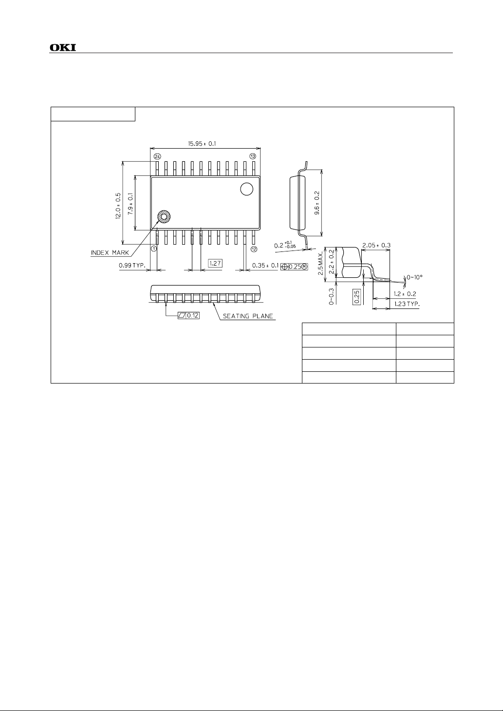
SOP24-P-430-1.27-K
Mirror finish
(Unit : mm)
Package material
Lead frame material
Pin treatment
Solder plate thickness
Package weight (g)
Epoxy resin
42 alloy
Solder plating
5 mm or more
0.58 TYP.
Notes for Mounting the Surface Mount Type Package
The SOP, QFP, TSOP, SOJ, QFJ (PLCC), SHP and BGA are surface mount type packages, which
are very susceptible to heat in reflow mounting and humidity absorbed in storage.
Therefore, before you perform reflow mounting, contact Oki’s responsible sales person for the
product name, package name, pin number, package code and desired mounting conditions
(reflow method, temperature and times).
12/12
 Loading...