

Datasheet MSM64P155-003GS-BK, MSM64P155-xxxGS-BK, MSM64P155L-002GS-BK, MSM64P155-001GS-BK, MSM64P155L-xxxGS-BK Datasheet (OKI)
...Page 1

E2E0050-18-95
This version: Sep. 1998
MSM64P155/64P155L¡ Semiconductor
Preliminary
¡ Semiconductor
MSM64P155/64P155L
4-Bit Microcontroller with Built-in LCD Driver and Melody Circuit
GENERAL DESCRIPTION
The MSM64P155 (1.5 V)/64P155L (3.0 V) is a one-time-programmable ROM version product,
which has one-time PROM (OTP) as internal program memory. On the other hand, the
MSM64155 is a mask ROM-version product, which has mask ROM as internal program memory.
Unlike the mask ROM-version MSM64155 which has a P-well CMOS structure, the MSM64P155/
64P155L has been fabricated with the N-well CMOS-structured EPROM process technology.
Therefore, the MSM64P155/64P155L differs from the MSM64155 in the polarity of the power
supply for LCD bias generation and in the external circuit structure.
Unlike the mask ROM-version product, the MSM64P155/64P155L cannot be supplied in the
form of a chip. The MSM64P155/64P155L is an OTP-version product used to evaluate an
application program.
The MSM64P155/64P155L has two operation modes, microcontroller operation mode and
PROM mode. The microcontroller operation mode is used to operate the MSM64P155/64P155L
like a mask ROM-version product and the PROM mode is used to program or read the PROM.
FEATURES
• Operating range
Operating voltage (mask option) : 1.5 V/3.0 V
Operating frequency : 32.768 kHz crystal oscillation
Approx. 32 kHz RC oscillation
• Minimum instruction execution time : 91 ms
• General memory space : 4064 bytes (PROM)
• Local memory space : 256 nibbles
• LCD driver : 64
Common driver ¥ 4
Segment driver ¥ 60
1/4 duty, 1/3 bias; 240 segments (60 ¥ 4)
1/3 duty, 1/3 bias; 180 segments (60 ¥ 3)
• I/O port
Input-output port : 2 ports ¥ 4 bits (open-drain output/CMOS output
selectable; pull-down resistor input/high-impedance
input selectable)
Input port : 1 port ¥ 2 bits (pull-down resistor input/high-impedance
input selectable)
1 port ¥ 4 bits (pull-down resistor input/high-impedance
input selectable)
Output port : 1 port ¥ 4 bits (CMOS output)
• Event counter : 1 channel
• Melody output : 2
• Capture circuits : 2 channels
256 Hz, 128 Hz, 64 Hz, 32 Hz
1/29
Page 2

• Interrupt sources : 10 sources
External 4, time base 4, melody 2
(When TST3 = "1", six time base sources)
• Clock generation circuit (mask option) : Crystal/RC oscillation
• Package:
100-pin plastic QFP (QFP100-P-1420-0.65-BK)
Product name :
MSM64P155-001GS-BK (crystal oscillation, 1.5 V, blanked PROM)
MSM64P155L-002GS-BK (crystal oscillation, 3.0 V, blanked PROM)
MSM64P155-003GS-BK (RC oscillation, 1.5 V, blanked PROM)
MSM64P155L-004GS-BK (RC oscillation, 3.0 V, blanked PROM)
MSM64P155-xxxGS-BK (crystal/RC oscillation, 1.5 V, written PROM)
MSM64P155L-xxxGS-BK (crystal/RC oscillation, 3.0 V, written PROM)
xxx indicates a code number.
MSM64P155/64P155L¡ Semiconductor
2/29
Page 3
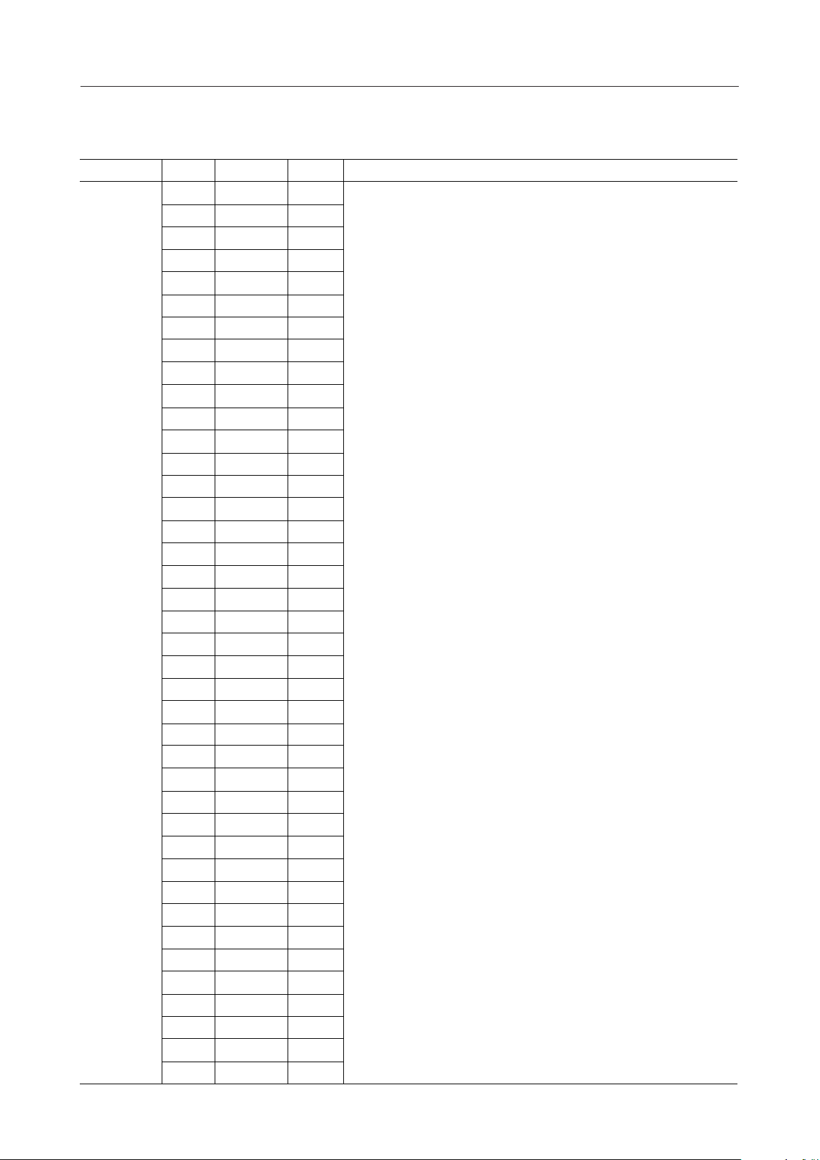
BLOCK DIAGRAM
BSRHALTMIEF
TR2 TR0 TR1
(4)
PCM PCL
PCH
ROM
4064B
MSM64P155/64P155L¡ Semiconductor
C2C1V
BIAS
DD3VDD2VDD1
COM1
COM2
COM3
COM4
OSC0
OSC1
RESET
TST1
TST2
TST3
V
C
BA HL XY
CLK
RST
TST
SS
BUP CAPR PORT2 EVENT PORT3 PORT4 PORT6 PORT7
ALU
(4) (4)
TIMING
CONTROLLER
TBC
INT
A8 to A11
A7 to A0
RAM
256N
DB7 to DB0
ROMRSP
4
IR
DECODER
IR
PORT ADDRESS
DB7 to DB0
(8)
INTC
(8)
PORT ADDRESS
INT INTINTINT
LCD
MD0
INT
MD1
INT
SEG0
SEG59
MD0
MD0
MD1
MD1
is the CPU core (nx-4/20).
P2.0
P2.1
P2.2
P2.3
P3.0
P3.1
P4.0
P4.1
P4.2
P4.3
P6.0
P6.1
P6.2
P6.3
P7.0
P7.1
P7.2
P7.3
3/29
Page 4
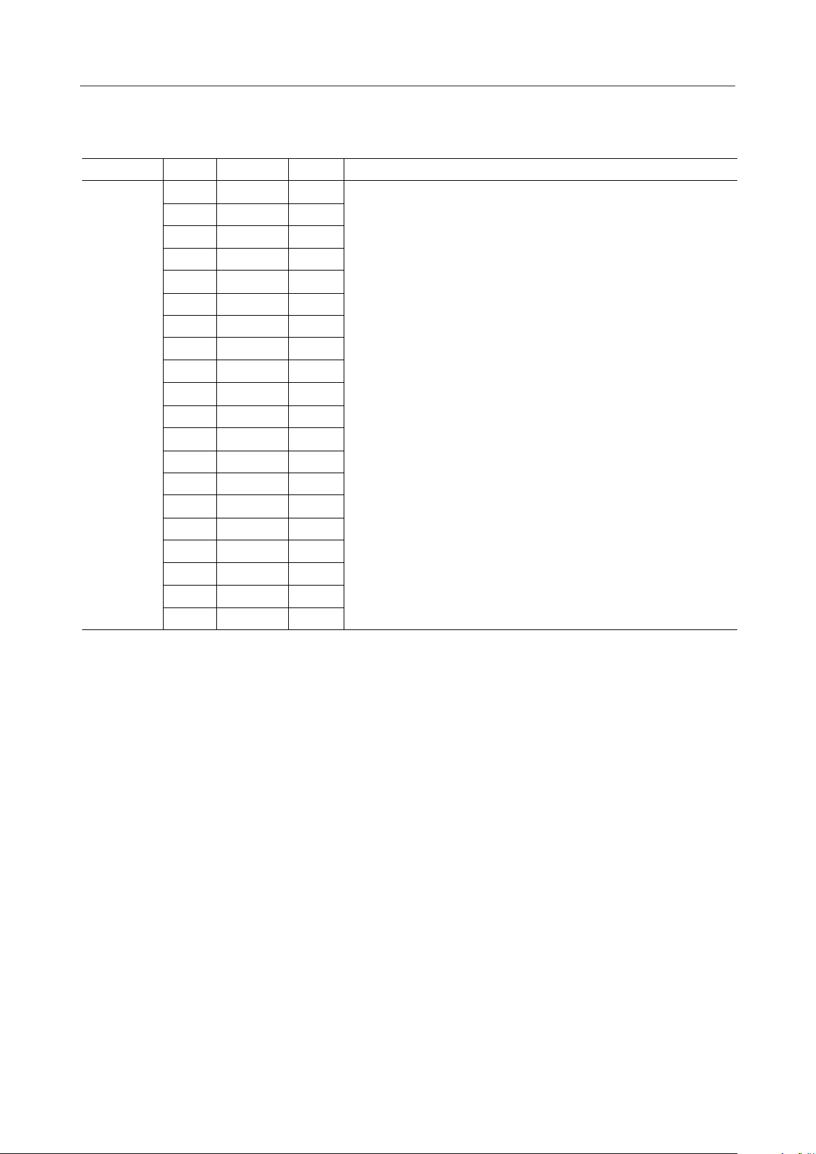
PIN CONFIGURATION (TOP VIEW)
DD3
DD2
DD1
V
100
V
V
98
99
C1
97
C2
96
COM1
95
COM3
COM2
93
94
SEG0
COM4
91
92
SEG2
SEG1
89
90
SEG4
SEG3
87
88
SEG6
SEG5
85
86
SEG8
SEG7
83
84
MSM64P155/64P155L¡ Semiconductor
SEG10
SEG9
81
82
RESET
OSC0
OSC1
V
PP
P2.3
P2.2
P2.1
P2.0
P3.1
P3.0
P4.3
P4.2
P4.1
P4.0
P6.3
P6.2
P6.1
P6.0
P7.3
P7.2
P7.1
P7.0
V
SS
MD0
MD0
MD1
MD1
TST3
TST2
TST1
1
2
3
4
5
6
7
8
9
10
11
12
13
14
15
16
17
18
19
20
21
22
23
24
25
26
27
28
29
30
80
79
78
77
76
75
74
73
72
71
70
69
68
67
66
65
64
63
62
61
60
59
58
57
56
55
54
53
52
51
SEG11
SEG12
SEG13
SEG14
SEG15
SEG16
SEG17
SEG18
SEG19
SEG20
SEG21
SEG22
SEG23
SEG24
SEG25
SEG26
SEG27
SEG28
SEG29
SEG30
SEG31
SEG32
SEG33
SEG34
SEG35
SEG36
SEG37
SEG38
SEG39
SEG40
32
31
34
33
37
36
35
40
39
38
43
42
41
46
45
44
49
48
47
(NC)
SEG42
SEG43
SEG44
SEG45
SEG46
SEG47
SEG48
SEG49
SEG50
SEG51
SEG52
SEG53
SEG54
SEG55
SEG56
SEG57
SEG58
SEG59
100-Pin Plastic QFP
Note: Pins marked as (NC) are no-connection pins which are left open.
50
SEG41
4/29
Page 5
PIN DESCRIPTIONS
Basic Functions
MSM64P155/64P155L¡ Semiconductor
Power
Supply
Oscillation
Test
Pin
23
100
99
98
97
96
4
2
3
30
29
28
Symbol
V
SS
V
DD1
V
DD2
V
DD3
C1
C2
V
PP
OSC0
OSC1
TST1
TST2
TST3
TypeFunction
—
Digital supply voltage (0 V)
—
Digital positive power supply (1.5 V spec.)
Description
Bias output for LCD driver (3.0 V spec.)
—
Digital positive power supply (3.0 V spec.)
Bias output for LCD driver (1.5 V spec.)
Bias output for LCD driver (+4.5 V)
—
—
Pins for connecting a capacitor for generating LCD driving bias
—
—
Positive power supply for writing programming data to PROM
(+12.5 V)
I
Clock oscillation pins:
Either a crystal (32.768 kHz) and a capacitor (10 to 30 pF) are
connected to these pins or a resistor (1 MW) is.
O
I
Input pins for test:
These pins are internally pulled down to V
I
When this pin is set to "H" level, the 256 Hz and 4 Hz interrupts are
I
SS
.
enabled, and then the MSM64P155 can be used as an OTP version
of the MSM64152A, MSM64153A, and MSM64158A.
RESET
1I
RESET
System reset input pin :
Setting this pin to "H" level puts this device into a reset state.
Then, setting this pin to "L" level starts executing an instruction from
address 000H.
This pin is internally connected to V
through a pull-down resistor.
SS
5/29
Page 6
Basic Functions (continued)
MSM64P155/64P155L¡ Semiconductor
Pin DescriptionTypeFunction
Ports 4-bit input port (port 2) :
10
14
13
12
11
18
17
16
15
22
21
20 P7.2
19
Melody
Drivers
LCD
Drivers
95
94
93
92
Symbol
8
7
6
5
9
P2.0
P2.1
P2.2
P2.3
P3.0
P3.1
P4.0
P4.1
P4.2
P4.3
P6.0
P6.1
P6.2
P6.3
P7.0
P7.1
P7.3
MD0
MD0
MD1
MD1
COM1
COM2
COM3
COM4
I
Select between pull-down resistor input and high impedance input
for each bit with the port 2 control register (P2CON).
When configured for secondary functions, an external interrupt and
capture circuit trigger input are allocated.
If P2.0 to P2.3 are set to "H" level, the device enters system reset
mode.
I 2-bit input port (port 3) :
Select between pull-down resistor input and high impedance input
with the port 3 control register (P3CON).
When configured for a secondary function, an external interrupt is
allocated to P3.0 and an event counter is allocated to P3.1.
O
4-bit output port (port 4) :
4-bit CMOS output port.
4-bit input-output port (port 6) :
I/O
Select between input and output, between pull-down resistor input
and high impedance input, and between open-drain output and CMOS
output with the port 6 control register (P6CON). When configured
for a secondary function, an external interrupt is allocated.
4-bit input-output port (port 7) :
I/O
Select between input and output, between pull-down resistor input
and high impedance input, and between open-drain output and CMOS
output with the port 7 control register (P7CON). When configured for
a secondary function, an external interrupt is allocated.
O Output pin of melody driver 0.25
O Inverted output pin of MD0 output.24
O Output pin of melody driver 1.26
O Inverted output pin of MD1 output.27
O
LCD common signal output pins.
O
O
O
6/29
Page 7
Basic Functions (continued)
MSM64P155/64P155L¡ Semiconductor
LCD
Drivers
Pin DescriptionTypeFunction
91
Symbol
SEG0
SEG1
SEG2
SEG3
SEG4
SEG5
SEG6
SEG7
SEG8
SEG9
SEG10
SEG11
SEG12
SEG13
SEG14
SEG15
SEG16
O
LCD segment signal output pins.
O90
O89
O88
O87
O86
O85
O84
O83
O82
O81
O80
O79
O78
O77
O76
O75
SEG17
SEG18
SEG19
SEG20
SEG21
SEG22
SEG23
SEG24
SEG25
SEG26
SEG27
SEG28
SEG29
SEG30
SEG31
SEG32
SEG33
SEG34
O74
O73
O72
O71
O70
O69
O68
O67
O66
O65
O64
O63
O62
O61
O60
O59
O58
O57
SEG35
SEG36
SEG37
SEG38
SEG39
O56
O55
O54
O53
O52
7/29
Page 8
Basic Functions (continued)
MSM64P155/64P155L¡ Semiconductor
LCD
Drivers
Pin DescriptionTypeFunction
51
39
38
37
36
35
34
33
32
31
Symbol
SEG40
SEG41
SEG42
SEG43
SEG44
SEG45
SEG46
SEG47
SEG48
SEG49
SEG50
SEG51
SEG52
SEG53
SEG54
SEG55
SEG56
SEG57
SEG58
SEG59
O
LCD segment signal output pins.
O50
O49
O48
O47
O46
O45
O44
O43
O42
O41
O
O
O
O
O
O
O
O
O
8/29
Page 9
Secondary Functions
MSM64P155/64P155L¡ Semiconductor
External
Interrupts
Pin DescriptionTypeFunction
10
18
17
16
15
22
21
20
Symbol
8
7
6
5
P2.0
P2.1
P2.2
P2.3
P3.0
P6.0
P6.1
P6.2
P6.3
P7.0
P7.1
P7.2
I
P2.0 to P2.3 secondary functions :
These are level-triggered external interrupt input pins.
Select interrupt enable/disable for each bit with the P2 interrupt
enable register (P2IE).
If P2.0 to P2.3 pins are set to "H" level for a minimum of 2 seconds,
the device enters system reset mode.
P2.0, P2.1 secondary functions :
trigger input pins for capture circuit.
I
P3.0 secondary function :
This is an input pin for external interrupt. This pin can receive an
interrupt at a rising edge, a falling edge, or at both rising and falling
edges.
I
P6.0 to P6.3 secondary functions :
These are level-triggered external interrupt input pins.
I
P7.0 to P7.3 secondary functions :
These are level-triggered external interrupt input pins.
Counter
Input
19
P7.3
9Event
P3.1
I
P3.1 secondary function :
Input port for event counter
9/29
Page 10

MSM64P155/64P155L¡ Semiconductor
PROM-Related Pins
The pins for writing program data of the MSM64P155/64P155L are shown below.
Programming
Pin DescriptionTypeFunction
23
100
99
30
29
91
Symbol
V
SS
V
DD1*
V
DD2*
4
1
V
PP
RESET
TST1
TST2
SEG0/D0
90 SEG1/D1
89 SEG2/D2
88 SEG3/D3
87 SEG4/D4
86 SEG5/D5
85 SEG6/D6
84 SEG7/D7
83 SEG8/CE
82 SEG9/OE
81 SEG10/A0
80 SEG11/A1
79 SEG12/A2
78 SEG13/A3
77 SEG14/A4
76 SEG15/A5
75 SEG16/A6
74 SEG17/A7
73 SEG18/A8
72 SEG19/A9
71 SEG20/A10
70 SEG21/A11
69
SEG22
O
0 V power supply
—
Positive power supply pin (+5 V)
—
Positive power supply pin (+5 V)
—
Power supply pin for programming PROM (+12.5 V)
I PROM programming setting pins.
When a "H" level is input to these pins, the device enters the PROM
mode.
Pins for writing or reading program data to and from PROM.I/O
I/O
PROM chip enable pin
I/O
PROM output enable signal
I
Program address input pins
I
Normally apply a "H" level to this pin.
* When in PROM mode, supply a 5 V power to both V
DD1
and V
DD2
.
10/29
Page 11

Handling When Specific Pins Are Not Used
MSM64P155/64P155L¡ Semiconductor
Symbol
TST1 to TST3
P2.0 to P2.3
P3.0, P3.1
P4.0 to P4.3
P6.0 to P6.3
P7.0 to P7.3
MD0, MD0
MD1, MD1
COM1 to COM4
SEG0 to SEG59
Recommended Pin Connection
Open
"L" level or open
"L" level or open
Open
In input mode : "L" level or open (Initial setting: input mode)
In output mode : Open
In input mode : "L" level or open (Initial setting: input mode)
In output mode : Open
Open
Open
Open
11/29
Page 12

MSM64P155/64P155L¡ Semiconductor
(1) For 1.5 V Specifications in the Microcontroller Operation Mode
Product Name: MSM64P155
ABSOLUTE MAXIMUM RATINGS
(V
Parameter Symbol Condition Rating Unit
Power Supply Voltage 1 V
Power Supply Voltage 2 V
Power Supply Voltage 3 V
Input Voltage 1 V
Output Voltage 1 V
Output Voltage 2 V
Output Voltage 3 V
Storage Temperature T
DD1
DD2
DD3
IN1
OUT1
OUT2
OUT3
STG
Ta = 25°C –0.3 to +2.0 V
Ta = 25°C –0.3 to +4.0 V
Ta = 25°C –0.3 to +5.5 V
V
input, Ta = 25°C –0.3 to V
DD1
V
output, Ta = 25°C –0.3 to V
DD1
V
output, Ta = 25°C –0.3 to V
DD2
V
output, Ta = 25°C –0.3 to V
DD3
—
–55 to +150 °C
+ 0.3 V
DD1
+ 0.3 V
DD1
+ 0.3 V
DD2
+ 0.3 V
DD3
SS
= 0 V)
RECOMMENDED OPERATING CONDITIONS
Parameter Symbol Condition Range Unit
Operating Temperature T
Operating Voltage V
Crystal Oscillation Frequency
External RC Oscillator Resistance
R
op
DD1
f
XT
OS
—
—
—
(V
= 0 V)
SS
0 to +65 °C
1.4 to 1.7 V
30 to 35 kHz
1M ±10% W—
12/29
Page 13

ELECTRICAL CHARACTERISTICS
DC Characteristics
(V
Parameter
V
Voltage V
DD2
Voltage V
V
DD3
Crystal Oscillation
Start Voltage
Crystal Oscillation
Hold Voltage
External Crystal Oscillator
Capacitance
Internal Crystal Oscillator
Capacitance
RC Oscillation Frequency
Symbol Condition
DD2
DD3
V
STA
V
HOLD
C
G
C
D
f
CR
= 0 V, V
SS
, C
= 1 mF Cb = 0.1 mF
a
12
= 1 mF Cb = 0.1 mF
12
= 1.5 V, Ta = 0 to +65°C unless otherwise specified)
DD1
Oscillation start time:
within 5 seconds
—
—
= 1 MW
R
OS
MSM64P155/64P155L¡ Semiconductor
Max.Typ.Min.
Unit
2.8 3.2 VC
3.0
4.54.3 4.7 VCa, C
1.47
1.40——
10 30 pF
—V
—V
—
1510 20 pF—
4015 75 kHz
Measuring
Circuit
1a
DC Characteristics (32.768 kHz Crystal Oscillation)
(V
= 0 V, V
SS
= 1.5 V, Ta = 0 to +65°C unless otherwise specified)
DD1
Parameter Symbol Condition
Supply Current 1 I
Supply Current 2 I
DD1
DD2
CPU in the HALT mode
CPU in the operating mode
DC Characteristics (RC Oscillation)
(V
SS
Parameter Symbol Condition
Supply Current 1 I
Supply Current 2 I
= 0 V, V
DD1
DD2
= 1.5 V, R
DD1
CPU in the HALT mode
CPU in the operating mode
= 1 MW, Ta = 0 to +65°C unless otherwise specified)
OS
Min.
—
—
Min.
—
—
Typ.
Max.
2.0
75 100
Typ.
Max.
3.0
100 200
Unit
10 mA
mA
Unit
20 mA
mA
Measuring
Circuit
1a
Measuring
Circuit
1b
13/29
Page 14

DC Characteristics (continued)
MSM64P155/64P155L¡ Semiconductor
Parameter Symbol Condition
Output Current 1
(P4.0 to P4.3)
(MD0, MD0)
(MD1, MD1)
Output Current 2
(SEG0 to SEG59)
(COM1 to COM4)
Output Current 3
(P6.0 to P6.3)
(P7.0 to P7.3)
Output Leakage
(P6.0 to P6.3)
(P7.0 to P7.3)
Input Current 1
(P2.0
to
P2.3)
(P3.0
,
P3.1)
(P6.0
to
P6.3)
(P7.0
to
P7.3)
(V
= 0 V, V
SS
= 1.5 V, V
DD1
I
I
I
OH1
I
OL1
I
OH2
I
OMH2
OMH2S
I
OML2
OML2S
I
OL2
I
OH3
I
OL3
I
OOH
I
OOL
I
IH1
I
IH1Z
I
IL1
= 3.0 V, V
DD2
= V
OH1
DD1
= +0.5 V 0.1
OL1
V
= V
OH2
DD3
V
= V
OMH2
DD2
V
= V
OMH2S
DD2
V
= V
OML2
DD1
V
= V
OML2S
DD1
V
= +0.2 V (VSS level)
OL2
= V
OH3
DD1
= +0.5 V
OL3
= V
OH
DD1
= V
OL
SS
= V
V
IH1
DD1
= 4.5 V, Ta = 0 to +65°C unless otherwise specified)
DD3
– 0.5 V –2.0
– 0.2 V (V
+ 0.2 V (V
– 0.2 V (V
+ 0.2 V (V
– 0.2 V (V
DD3
DD2
DD1
DD2
DD1
level)
level)
level)
level)
level)
– 0.5 V
(when pulled down)
= V
V
IH1
DD1
(in a high impedance state)
= V
IL1
SS
—
4.0
—
4.0
—
4.0
–5.0
0.1 mAV
—
–0.3 mAV
1.0
0
–1.0
Max.Typ.Min.
–0.1 mAV
–0.7
0.7 2.0 mAV
–4.0 mA
—
—
—
–4.0 mA
—
—
—
–4.0 mA
—
—
—
–0.3 mAV
–2.1
2.00.7
—
0.3 mAV
—
—
10 100 mA
1.0 mA
—
0 mAV
—
Unit
mA
mA
mA
Measuring
Circuit
2
Input Current 2
(TST1, TST2)
Input Current 3
(TST3)
Input Current 4
(RESET)
Input Voltage 1
(P2.0 to P2.3)
(P3.0, P3.1)
(P6.0 to P6.3)
(P7.0 to P7.3)
(TST1, TST2, TST3)
(RESET)
I
IH2
I
IL2
I
IH3
I
IL3
I
IH4
I
IL4
V
IH1
IH2
IL2
IH3
IL3
IH4
IL4
= V
= V
= V
= V
= V
= V
DD1
SS
DD1
SS
DD1
SS
—
0.3 0.75
–1.0
0.3
0
15
–1
–0.3
—
1.0
—
40
—
—
1.5 mAV
0
mAV
5.0 mAV
mAV
1.0
100 mAV
0
mAV
0V
3
4
—
V
IL1
—
–1.2
V–1.5
14/29
Page 15

Measuring circuit 1a
MSM64P155
OSC1
OSC0
C1
C2
MSM64P155/64P155L¡ Semiconductor
Crystal
32.768 kHz
C
12
C
G
V
SS
V
SSVDD1VDD2
A V V
Measuring circuit 1b
V
SSVDD1VDD2
V
C
a
C
MSM64P155
V
b
DD3
DD3
OSC1
OSC0
C1
C2
Ca, C
C
b
C
G
R
OS
C
12
12
: 1 mF
: 0.1 mF
: 15 pF
C
a
C
b
A V V
C
a
Cb, C
R
OS
12
: 20 mF
: 0.1 to 0.2 mF
: 1 MW
15/29
Page 16

Measuring circuit 2
MSM64P155/64P155L¡ Semiconductor
(*2)
V
IH
(*1)
V
IL
Measuring circuit 3
(*3)
INPUT
MSM64P155
V
SSVDD1VDD2VDD3
OUTPUT
A
A
OUTPUT
MSM64P155
INPUT
V
SSVDD1VDD2VDD3
16/29
Page 17

Measuring circuit 4
MSM64P155/64P155L¡ Semiconductor
V
IH
(*3)
V
IL
INPUT
V
SSVDD1VDD2VDD3
MSM64P155
*1 Input logic circuit to determine the specified measuring conditions.
*2 Measured at the specified output pins.
*3 Measured at the specified input pins.
OUTPUT
Waveform
Monitoring
17/29
Page 18

MSM64P155/64P155L¡ Semiconductor
(2) For 3.0 V Specifications in the Microcontroller Operation Mode
Product Name: MSM64P155L
ABSOLUTE MAXIMUM RATINGS
Parameter Symbol Condition Rating Unit
Power Supply Voltage 1 V
Power Supply Voltage 2 V
Power Supply Voltage 3 V
Input Voltage 1 V
Output Voltage 1 V
Output Voltage 2 V
Storage Temperature T
DD1
DD2
DD3
IN1
OUT1
OUT2
STG
RECOMMENDED OPERATING CONDITIONS
Parameter Symbol Condition Range Unit
Operating Temperature
Operating Voltage
Crystal Oscillation Frequency
External RC Oscillator Resistance
T
op
V
DD2
f
XT
R
OS
Ta = 25°C –0.3 to +2.0 V
Ta = 25°C –0.3 to +4.0 V
Ta =25°C –0.3 to +5.5 V
V
input, Ta = 25°C –0.3 to V
DD2
V
output, Ta = 25°C –0.3 to V
DD2
V
output, Ta = 25°C –0.3 to V
DD3
—
—
—
—
—
–55 to +150 °C
0 to +65
2.7 to 3.5
30 to 66
1M ±10%
+ 0.3 V
DD2
+ 0.3 V
DD2
+ 0.3 V
DD3
(V
(V
SS
SS
= 0 V)
= 0 V)
°C
V
kHz
W
18/29
Page 19

ELECTRICAL CHARACTERISTICS
DC Characteristics
Parameter Symbol Condition
V
Voltage V
DD1
V
Voltage V
DD3
Crystal Oscillation Start Voltage
Crystal Oscillation Hold Voltage
External Crystal Oscillator
Capacitance
V
V
HOLD
DD1
DD3
STA
C
G
(V
= 0 V, V
SS
= 1 mF Cb, C
a
= 3.0 V, Ta = 0 to +65°C unless otherwise specified)
DD2
12
12
Oscillation start time:
within 5 seconds
—
—
= 0.1 mF
= 0.1 mF
MSM64P155/64P155L¡ Semiconductor
Max.Typ.Min.
Unit
1.5
1.3 1.7 VC
4.54.3 4.7 VCa = 1 mF Cb, C
—
2.7
2.7
10 30 pF
—
—
—V
—V
Measuring
Circuit
1a
Internal Crystal Oscillator
Capacitance
RC Oscillation Frequency
C
D
f
CR
= 1 MW
OS
—
DC Characteristics (32.768 kHz Crystal Oscillation)
(V
= 0 V, V
SS
= 3.0 V, Ta = 0 to +65°C unless otherwise specified)
DD2
Parameter Symbol Condition
Supply Current 1 I
Supply Current 2 I
DD1
DD2
CPU in the HALT mode
CPU in the operating mode
DC Characteristics (RC Oscillation)
(V
Parameter Symbol Condition
Supply Current 1 I
Supply Current 2 I
DD1
DD2
= 0 V, V
SS
CPU in the HALT mode
CPU in the operating mode
= 3.0 V, Ta = 0 to +65°C unless otherwise specified)
DD2
—
—
—
—
1510 20 pF
4015 75 kHzR
Unit
Max.Typ.Min.
1.0
5.0 mA
35 50
Unit
Max.Typ.Min.
3.0
15 mA
50 100
mA
Measuring
mA
Measuring
Circuit
1a
Circuit
1b
19/29
Page 20

DC Characteristics (continued)
(V
Parameter
= 0 V, V
SS
= 1.5V, V
DD1
Symbol Condition
DD2
= 3.0 V, V
MSM64P155/64P155L¡ Semiconductor
= 4.5 V, Ta = 0 to +65°C unless otherwise specified)
DD3
Unit
Measuring
Circuit
Max.Typ.Min.
Output Current 1
(P4.0 to P4.3)
(MD0, MD0)
(MD1, MD1)
Output Current 2
(SEG0 to SEG59)
(COM1 to COM4)
Output Current 3
(P6.0 to P6.3)
(P7.0 to P7.3)
Output Leakage Current
(P6.0 to P6.3)
(P7.0 to P7.3)
Input Current 1
(P2.0
to
P2.3)
,
P3.1)
(P3.0
to
to
P6.3)
P7.3)
(P6.0
(P7.0
Input Current 2
(TST1, TST2)
Input Current 3
(TST3)
Input Current 4
(RESET)
Input Voltage 1
(P2.0 to P2.3)
(P3.0, P3.1)
(P6.0 to P6.3)
(P7.0 to P7.3)
(TST1, TST2, TST3)
(RESET)
I
OH1
I
OL1
I
OH2
I
OMH2
I
OMH2S
I
OML2
I
OML2S
I
OL2
I
OH3
I
OL3
I
OOH
I
OOL
I
IH1
I
IH1Z
I
IL1
I
IH2
I
IL2
I
IH3
I
IL3
I
IH4
I
IL4
V
IH1
V
IL1
= V
OH1
= +0.5 V 0.7
OL1
V
= V
OH2
V
OMH2
V
OMH2S
V
OML2
V
OML2S
V
= +0.2 V (VSS level)
OL2
OH3
= +0.5 V
OL3
= V
OH
= V
OL
V
= V
IH1
– 0.5 V –6.0
DD2
– 0.2 V (V
DD3
= V
+ 0.2 V (V
DD2
= V
– 0.2 V (V
DD2
= V
+ 0.2 V (V
DD1
= V
– 0.2 V (V
DD1
= V
– 0.5 V
DD2
DD2
SS
DD2
DD3
DD2
DD2
DD1
DD1
level)
level)
level)
level)
level)
(when pulled down)
= V
V
IH1
DD2
(in a high impedance state)
= V
IL1
SS
= V
IH2
DD2
= V
IL2
SS
= V
IH3
DD2
= V
IL3
SS
= V
IH4
DD2
= V
IL4
SS
—
—
–2.0
2.0 6.0 mAV
—
—
4.0
—
—
—
—
4.0
—
—
4.0
—
–18
–6.0
0.7V
—
—
–0.3V
—
100 300 mA
50
0
–1.0——
0.75 1.5
—
–1.0
20
80
–1.0
—
40
80
—
–1.0
2.4
—
—
–0.7 mAV
–4.0
—
–4.0
—
–4.0
—
–2.0V
6.01.6
0.3V
—
1.0 mA
0 mAV
3.0 mAV
0
200 mAV
0
200 mAV
0
3.0 V
0.6
mA
mA
mA
mA
mA
mA
mA
mA
mA
mA
mAV
mAV
mAV
V0
2
3
4
20/29
Page 21

Measuring circuit 1a
V
SSVDD2VDD1
MSM64P155L
V
DD3
OSC1
OSC0
C1
C2
MSM64P155/64P155L¡ Semiconductor
Crystal
32.768 kHz
C
12
C
G
V
SS
A V V
Measuring circuit 1b
V
SSVDD2VDD1
C
a
C
b
MSM64P155L
V
DD3
OSC1
OSC0
C1
C2
C
a
Cb, C
C
G
R
OS
C
12
12
: 1 mF
: 0.1 mF
: 15 pF
C
a
C
b
A V V
C
a
Cb, C
R
OS
12
: 1 mF
: 0.1 mF
: 1 MW
21/29
Page 22

Measuring circuit 2
MSM64P155/64P155L¡ Semiconductor
(*2)
V
IH
(*1)
V
IL
Measuring circuit 3
(*3)
INPUT
MSM64P155L
V
SSVDD1VDD2VDD3
OUTPUT
A
A
OUTPUT
MSM64P155L
INPUT
V
SSVDD1VDD2VDD3
22/29
Page 23

Measuring circuit 4
MSM64P155/64P155L¡ Semiconductor
V
IH
(*3)
V
IL
INPUT
V
SSVDD1VDD2VDD3
MSM64P155L
*1 Input logic circuit to determine the specified measuring conditions.
*2 Measured at the specified output pins.
*3 Measured at the specified input pins.
OUTPUT
Waveform
Monitoring
23/29
Page 24

MSM64P155/64P155L¡ Semiconductor
(3) PROM Operations (Common to 1.5 V and 3.0 V Specifications)
ABSOLUTE MAXIMUM RATINGS
Parameter Symbol Condition Rating Unit
V
= V
PROM Power Source Voltage
V
Program Voltage V
PROM Input Voltage V
PROM Output Voltage V
Storage Temperature T
CC
PP
I
O
STG
CC
Ta = 25°C
Ta = 25°C –0.3 to +14.0 V
Ta = 25°C
VCC output
Ta = 25°C
RECOMMENDED OPERATING CONDITIONS
Parameter Symbol Condition Range Unit
= V
DD1
VCC input
DD2
–0.3 to +6.7
–0.3 to V
V
SS1
+ 0.3 V
CC
– 0.3 to +0.3 V
–55 to +150 °C—
(V
(V
SS
SS
= 0 V)
V
= 0 V)
Operating Temperature T
Power Supply Voltage
V
CC
V
Power Supply Voltage
PP
Input Voltage
0 to +65 °C
4.75 to 5.25 V
4.75 to 5.25
12.0 to 13.0 VWhen data is written
4.0 to V
CC
0 to 1.0 V—V
V
V
CC
CC
= V
= V
—
DD1
DD1
= V
= V
DD2
DD2
op
V
CC
V
PP
V
IH
IL
V
When data is read
V
24/29
Page 25

ELECTRICAL CHARACTERISTICS
(1) Read Operation
DC Characteristics
(V
DD1
Parameter Symbol Condition
VCC Supply Voltage (Standby) I
VCC Supply Voltage (Operating) I
Input Voltage
Output Current
CC1
CC2
V
V
I
I
IH
IL
OH
OL
= V
= V
DD2
V
= V
CC
CE = V
= V
V
CC
CE = V
V
= V
CC
= 5 V ±5%, Ta = 25°C ±5°C unless otherwise specified)
PP
= V
DD1
IH
DD1
IL
DD1
= V
= V
DD2
DD2
DD2
—
= V
V
CC
V
OH
OL
= V
DD1
= V
CC
DD2
– 0.5 V
= 0.5 V 0.70.2
—
—
4.0
0
MSM64P155/64P155L¡ Semiconductor
Max.Typ.Min.
—
—
—
—
–0.7–2
35 mA
100 mA
V
CC
1.0 V
–0.2 mA
2mAV
Unit
V
AC Characteristics
Parameter Symbol Condition
Address Access Time t
CE Access Time t
OE Access Time t
Output Disable Time t
Measurement Conditions:
Input pulse level ............ 0.45 V to 4.55 V
Input rise/fall time ....... 5 ns
Threshold level ..............input 0.8 V, 2 V/output 0.8 V, 2 V
ACC
CE
OE
DF
(V
= 5 V ±5%, V
CC
OE = CE = V
OE = V
CE = V
CE = V
= VCC, Ta = 0 to +65°C unless otherwise specified)
PP
Max.Typ.Min.
IL
IL
IL
IL
—ns
—ns
—ns
0ns
—
—
—
—
120
120
50
40
Unit
25/29
Page 26

Address Input
CE
OE
MSM64P155/64P155L¡ Semiconductor
t
CE
Data Output
t
ACC
t
OE
t
DF
26/29
Page 27

(2) Write Operation
DC Characteristics
(V
= 0 V, V
SS
DD1
= V
DD2
Parameter Symbol Condition
Power Supply Current I
V
PP
VCC Power Supply Current I
Input Voltage
Output Current
AC Characteristics
(V
= 0 V, V
SS
DD1
= V
Parameter Symbol Condition
Address Setup Time t
OE Setup Time t
Data Setup Time t
Address Hold Time t
Data Hold Time t
OE Output Floating Delay Time t
Power Source Setup Time t
V
PP
Initial Program Pulse Width t
Additional Program Pulse Width t
OE Output Effective Delay Time t
Measurement Conditions:
Input pulse level ............ 0.45 V to 4.55 V
Input rise/fall time ....... less than 20 ns
Threshold level .............. input 0.8 V, 2 V/output 0.8 V, 2 V
= 5 V ±5%, V
PP
CC
V
IH
V
IL
I
OH
I
OL
= 5 V ±5%, V
DD2
AS
OES
DS
AH
DH
DFP
VS
PW
OPW
OE
= 12.5 V ±0.5 V, Ta = 25°C ±5°C unless otherwise specified)
PP
IL
= V
= V
DD1
DD1
= V
= V
DD2
DD2
CC
V
CC
—
= V
V
CC
V
OH
OL
= V
DD1
DD2
= VCC – 0.5 V
= 0.5 V 0.70.2
= 12.5 V ±0.5 V, Ta = 25°C ±5°C unless otherwise specified)
PP
—
—
—
—
—
—
—
V
= V
DD1
DD2
6 V ±0.25 V
V
= V
DD1
DD2
6 V ±0.25 V
——
MSM64P155/64P155L¡ Semiconductor
Max.Typ.Min.
—
—
4.0
0
—
—
—
—
–0.7–2.0
50
100
V
CC
1.0
–0.2
2.0
Max.Typ.Min.
2.0 ms
2.0 ms
2.0 ms
0 ms
2.0 ms
0ns130
2.0 ms
—
—
—
—
—
—
—
—
—
—
—
—
—
0.95 ms1.0 1.05
2.85 ms78.75
—
—
Unit
Unit
mACE = V
mAV
V
V
mA
mAV
ns150
27/29
Page 28

MSM64P155/64P155L¡ Semiconductor
Address Input
Data Input-Output
V
PP
CE
OE
Address N
t
AS
Data Input Data Output
t
PW
DH
t
OES
t
DS
t
VS
t
t
OPW
t
OE
t
t
AH
DFP
28/29
Page 29

PACKAGE DIMENSIONS
QFP100-P-1420-0.65-BK
Mirror finish
MSM64P155/64P155L¡ Semiconductor
(Unit : mm)
Package material
Lead frame material
Pin treatment
Solder plate thickness
Package weight (g)
Epoxy resin
42 alloy
Solder plating
5 mm or more
1.29 TYP.
Notes for Mounting the Surface Mount Type Package
The SOP, QFP, TSOP, SOJ, QFJ (PLCC), SHP and BGA are surface mount type packages, which
are very susceptible to heat in reflow mounting and humidity absorbed in storage.
Therefore, before you perform reflow mounting, contact Oki’s responsible sales person for the
product name, package name, pin number, package code and desired mounting conditions
(reflow method, temperature and times).
29/29
 Loading...