

Datasheet MSM64164C-xxxGS-K, MSM64164C-xxx, MSM64164C-xxxGS-BK, MSM64164C-xxxTS-K Datasheet (OKI)
Page 1

E2E0035-38-94
¡ Semiconductor MSM64164C
¡ Semiconductor
This version: Sep. 1998
Previous version: Apr. 1998
MSM64164C
4-Bit Microcontroller with Built-in RC Oscillation Type A/D Converter and LCD Driver
GENERAL DESCRIPTION
The MSM64164C is a low power 4-bit microcontroller that employs Oki's original CPU core nX4/20.
The MSM64164C is best suitable for applications such as low power, high precision thermometers and hygrometers.
The MSM64P164 is a one-time-programmable ROM-version product having one-time PROM
(OTP) as internal program memory.
The MSM64P164 is used to evaluate the software development.
The MSM64P164 differs from the MSM64164C in the polarity of the power supply.
FEATURES
• Operating range
Operating frequencies : 32.768 kHz, 400 kHz
Operating voltage : 1.25 to 1.7 V (1.5 V spec.)
2.0 to 3.5 V (3 V spec.)
2.2 to 3.5 V (3 V spec., 1/2 duty)
Operating temperature : –40 to +85°C
• Memory space
Internal program memory : 4064 bytes
Internal data memory : 256 nibbles
• Minimum instruction execution time : 7.5 ms @ 400 kHz
91.6 ms @ 32.768 kHz
• RC oscillation type A/D converter : 2 channels
Time dividing 2-channel method
• Serial port : Synchronous 8-bit transfer
• LCD driver : 34 outputs; duty ratio switchable by software
(1) At 1/4 duty and 1/3 bias : 120 segments (max)
(2) At 1/3 duty and 1/3 bias : 93 segments (max)
(3) At 1/2 duty and 1/2 bias : 64 segments (max)
• Buzzer driver : 1 output (4 output modes selectable)
• Capture circuit : 2 channels
• Watchdog timer
• Clock : 32.768 kHz crystal oscillator and 400 kHz RC
oscillator (with an external resistor)
CPU clock : 32.768 kHz/400 kHz (switchable by software)
Time base clock : 32.768 kHz
• Power supply voltage : 1.5 V/3 V (selectable by mask option)
• I/O port
Input-output port : 3 ports ¥ 4 bits
Input port : 1 port ¥ 4 bits
Output port : 1 port ¥ 4 bits
(8 out of the 34 LCD driver outputs can be used
as output-only ports by mask option.)
1/41
Page 2

¡ Semiconductor MSM64164C
• Interrupt sources
External interrupt : 2 sources
Internal interrupt : 8 sources
• Package options:
80-pin plastic QFP (QFP80-P-1420-0.80-BK) : (Product name : MSM64164C-¥¥¥GS-BK)
80-pin plastic QFP (QFP80-P-1414-0.65-K) : (Product name : MSM64164C-¥¥¥GS-K)
80-pin plastic TQFP (TQFP80-P-1212-0.50-K) : (Product name : MSM64164C-¥¥¥TS-K)
Chip : (Product name : MSM64164C-¥¥¥)
¥¥¥ indicates a code number.
• OTP version
The MSM64P164 has one-time PROM (OTP) as internal program memory and is used to
evaluate the software development.
The MSM64P164 differs from the MSM64164C in the polarity of the power supply and
operating voltage.
Refer to the "MSM64P164 User's Manual" for details.
2/41
Page 3
¡ Semiconductor MSM64164C
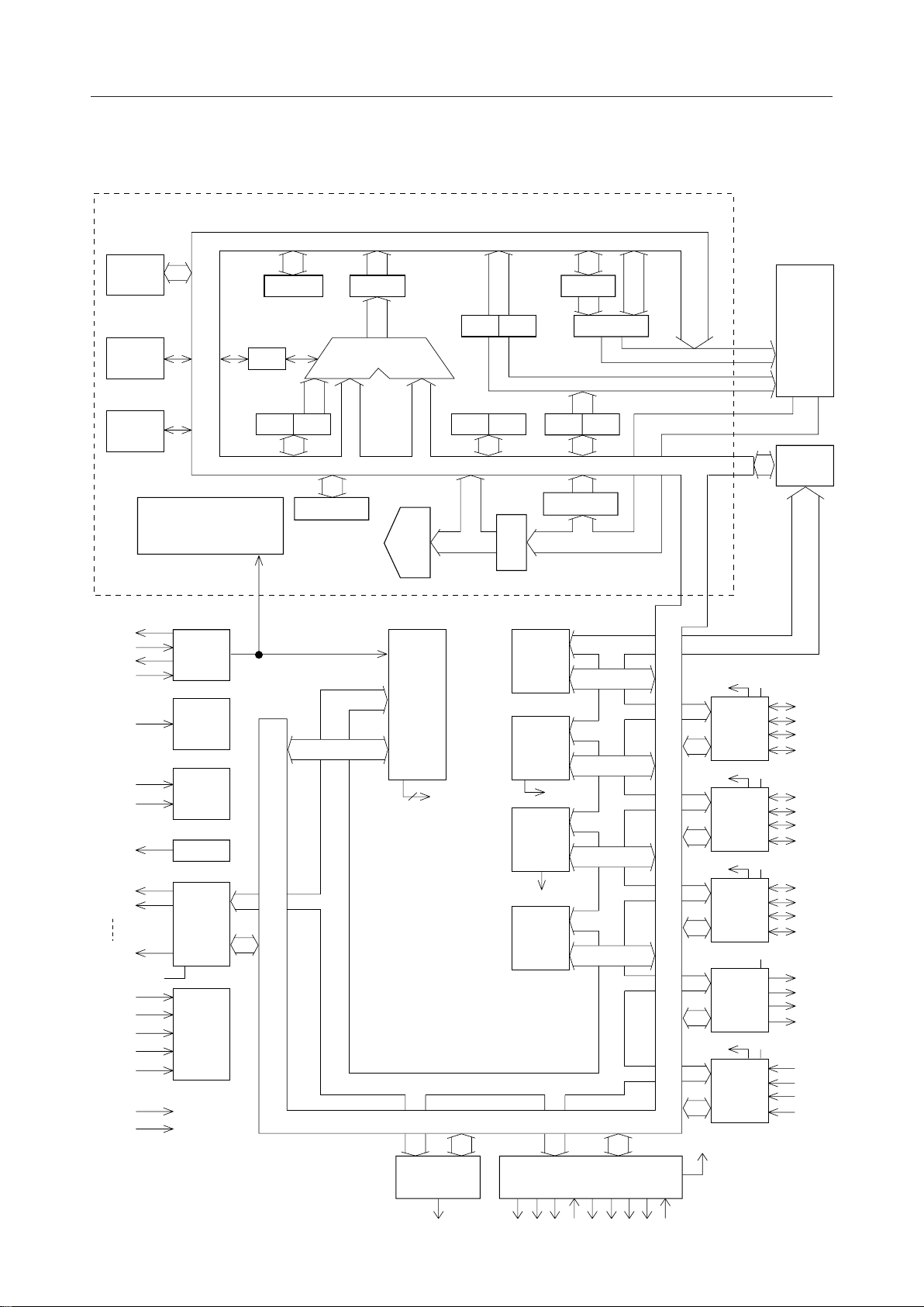
BLOCK DIAGRAM
CPU CORE: nX-4/20
OSC2
OSC1
XT
XT
RESET
TST1
TST2
V
SSL
L0
L1
L33
V
SS1
V
SS2
V
SS3
C1
C2
V
DD
V
SS
BSR
HALT
MIEF
CONTROLLER
V
SS
TIMING
2CLK
RSTG
TST
VR
LCD
BIAS
TR2 TR0
(4)
C
BA H L XY
ALU
(4) (4)
PCM
PCL
TR1
PCH
DB7 to DB0 (8)
SP
IR
IR
ROMR
DECODER
TBC
INTC
WDT
5
INT
INT
SIOP
INT
CAPR
PORT ADDRESS
DB7 to DB0
(8)
A11 to A8
A7 to A0
INT
INT
PORT4
INT
PORT3
INT
PORT2
PORT1
INT
PORT0
ROM
4064B
RAM
256N
V
SS
P4.3
P4.2
P4.1
P4.0
V
SS
P3.3
P3.2
P3.1
P3.0
V
SS
P2.3
P2.2
P2.1
P2.0
V
SS
P1.3
P1.2
P1.1
P1.0
V
SS
P0.3
P0.2
P0.1
P0.0
BD
RT1
RS1
CS1
ADCBD
IN1
RT0
RS0
CRT0
CS0
IN0
3/41
Page 4
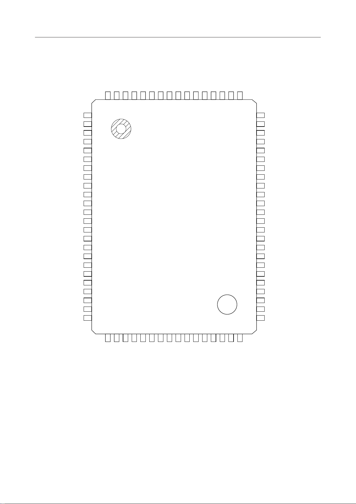
¡ Semiconductor MSM64164C
PIN CONFIGURATION (TOP VIEW)
DD
OSC2
OSC1
V
XT
XT
RESET
TST1
TST2
P1.0
P1.1
P1.2
P1.3
P0.0
P0.2
79
P0.1
78
77
76
75
74
73
72
71
70
69
68
67
66
65
P0.3
80
L0
L1
L2
L3
L4
L5
L6
L7
L8
L9
L10
L11
L12
L13
L14
L15
L16
P2.0
P2.1
P2.2
P2.3
P3.0
P3.1
P3.2
10
11
12
13
14
15
16
17
18
19
20
21
22
23
24
1
2
3
4
5
6
7
8
9
64
63
62
61
60
59
58
57
56
55
54
53
52
51
50
49
48
47
46
45
44
43
42
41
L33/P6.3
L32/P6.2
L31/P6.1
L30/P6.0
L29/P5.3
L28/P5.2
L27/P5.1
L26/P5.0
L25
L24
L23
L22
L21
L20
L19
L18
L17
C2
C1
V
SS3
V
SS2
V
SS
V
SS1
RT1
40
39
38
37
36
35
34
33
32
31
30
29
28
27
26
25
P3.3
P4.0
P4.1
P4.2
P4.3
BD
SSL
V
V
DD
RT0
CRT0
RS0
CS0
IN0
IN1
CS1
RS1
(QFP80-P-1420-0.80-BK)
80-Pin Plastic QFP
Note: Because pin 32 and pin 67 are internally connected with each other, VDD can be supplied
from either pin 32 or pin 67.
4/41
Page 5
¡ Semiconductor MSM64164C
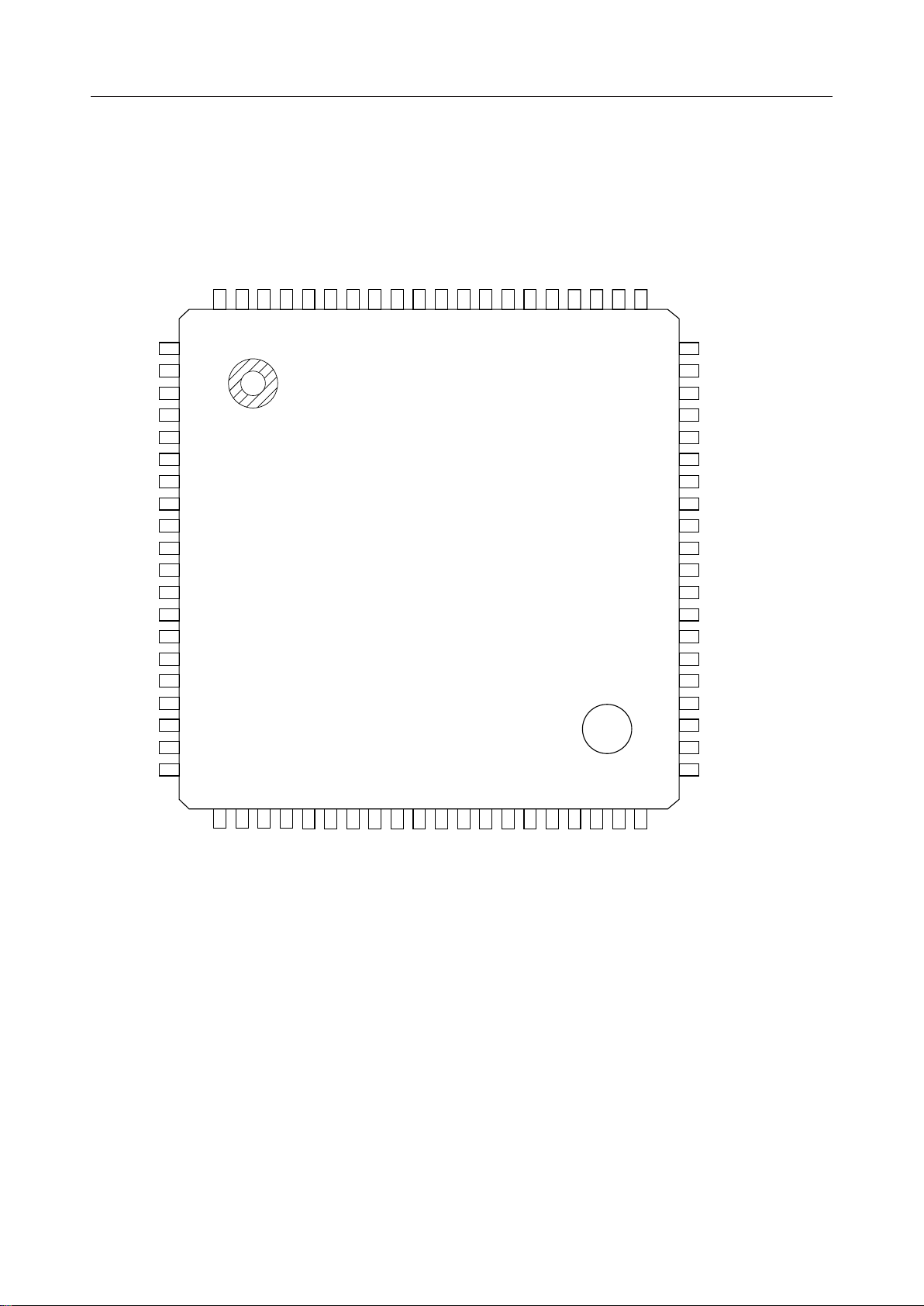
PIN CONFIGURATION (TOP VIEW) (continued)
VDDXT
XT
RESET
TST1
TST2
P1.0
P1.1
P1.2
P1.3
P0.0
P0.1
P0.2
P0.3
L1
80
L0
79
78
77
76
75
74
73
72
71
70
69
68
67
66
65
OSC1
64
63
L33/P6.3
OSC2
62
L32/P6.2
61
L2
L3
L4
L5
L6
L7
L8
L9
L10
L11
L12
L13
L14
L15
L16
P2.0
P2.1
P2.2
P2.3
P3.0
10
11
12
13
14
15
16
17
18
19
20
1
2
3
4
5
6
7
8
9
59
57
55
53
52
L31/P6.160
L30/P6.0
L29/P5.358
L28/P5.2
L27/P5.156
L26/P5.0
L2554
L24
L23
L2251
50
L21
49
L20
48
L19
47
L18
L1746
45
C2
44
C1
43
V
SS3
42
V
SS2
41
V
SS
21
P3.1
22
P3.2
23
P3.3
24
P4.0
25
P4.1
33
32
31
30
29
28
27
26
DD
BD
SSL
V
RT0
P4.2
P4.3
V
CRT0
RS0
(QFP80-P-1414-0.65-K)
80-Pin Plastic QFP
34
CS0
35
IN0
36
IN1
37
CS1
38
RS1
39
RT1
40
V
SS1
5/41
Page 6
¡ Semiconductor MSM64164C
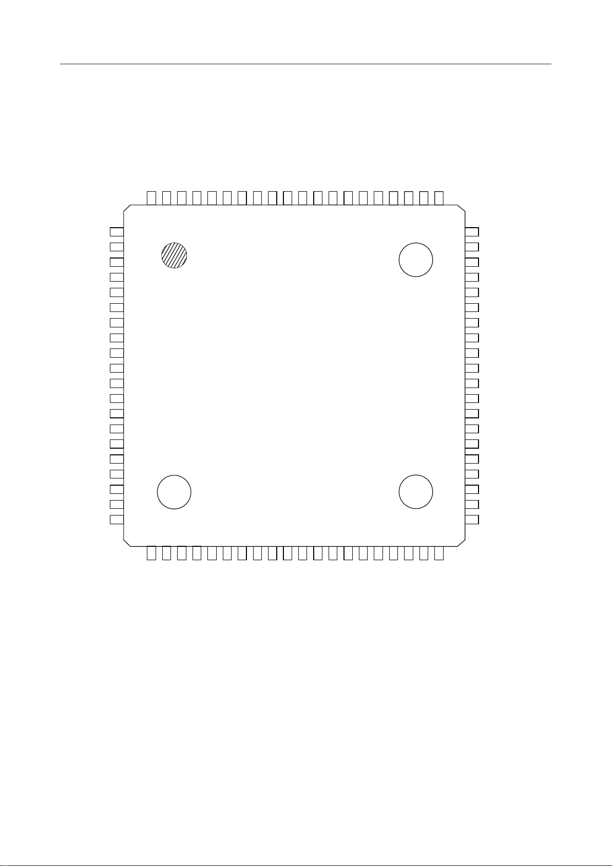
PIN CONFIGURATION (TOP VIEW) (continued)
VDDXT
XT
RESET
TST1
TST2
P1.0
P1.1
P1.2
P1.3
P0.0
P0.1
P0.2
L0
79
P0.3
78
77
76
75
74
73
72
71
70
69
68
67
66
65
OSC1
64
OSC2
63
L32/P6.2
L33/P6.3
61
62
L1
80
L2
L3
L4
L5
L6
L7
L8
L9
L10
L11
L12
L13
L14
L15
L16
P2.0
P2.1
P2.2
P2.3
P3.0
10
11
12
13
14
15
16
17
18
19
20
1
2
3
4
5
6
7
8
9
60
59
58
57
56
55
54
53
52
51
50
49
48
47
46
45
44
43
42
41
L31/P6.1
L30/P6.0
L29/P5.3
L28/P5.2
L27/P5.1
L26/P5.0
L25
L24
L23
L22
L21
L20
L19
L18
L17
C2
C1
V
SS3
V
SS2
V
SS
21
P3.1
22
P3.2
23
P3.3
24
P4.0
32
31
30
29
28
27
26
25
P4.1
P4.2
P4.3
BD
SSL
V
DD
V
RT0
CRT0
(TQFP80-P-1212-0.50-K)
80-Pin Plastic TQFP
33
RS0
34
CS0
35
IN0
36
IN1
37
CS1
38
RS1
39
RT1
40
SS1
V
6/41
Page 7
¡ Semiconductor MSM64164C
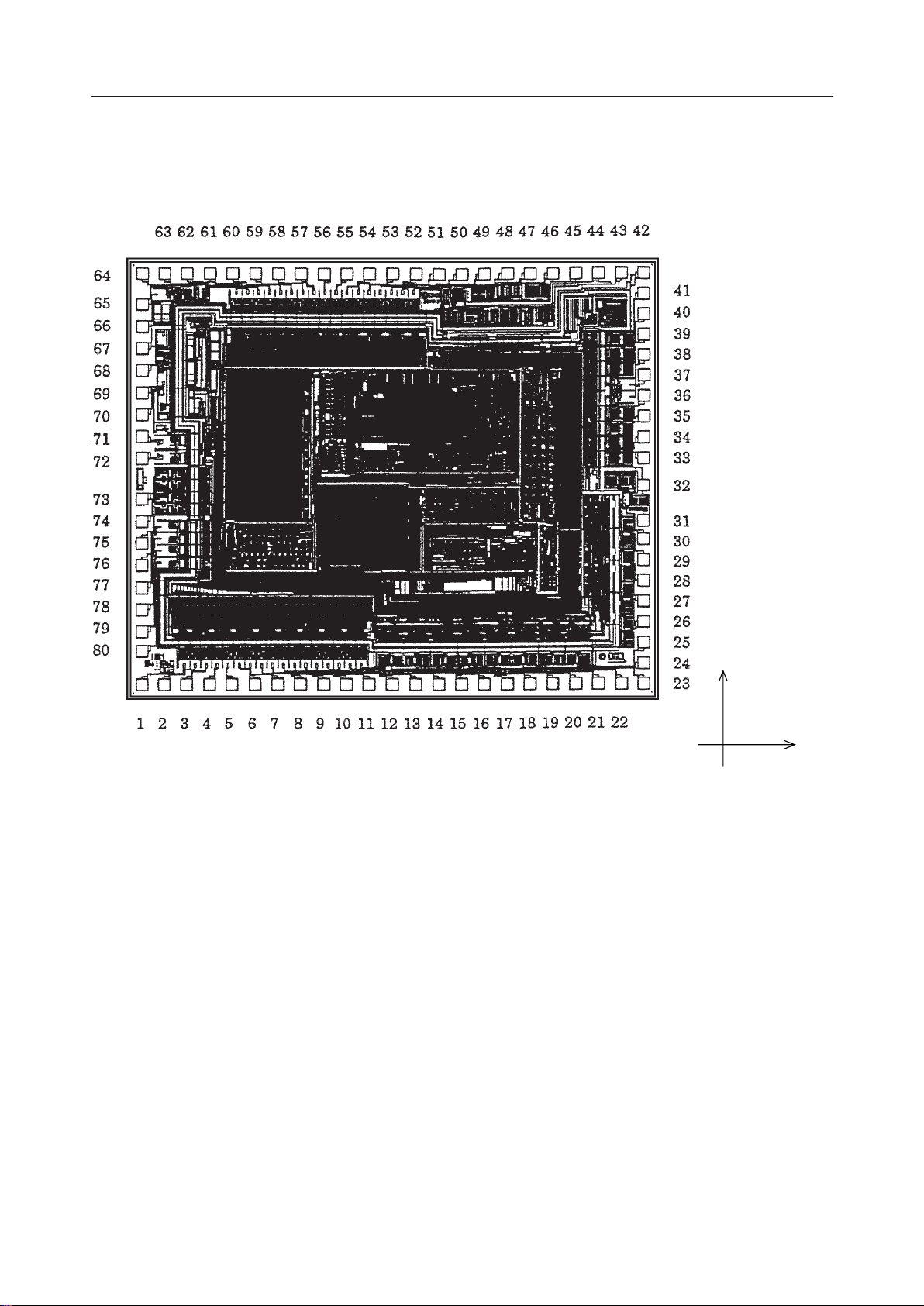
PAD CONFIGURATION
Pad Layout
Chip Size : 5.39 mm ¥ 4.48 mm
Chip Thickness : 350 mm (typ.)
Coordinate Origin : Chip center
Pad Hole Size : 100 mm ¥ 100 mm
Pad Size : 120 mm ¥ 120 mm
Minimum Pad Pitch : 180 mm
Note: The chip substrate voltage is VDD.
Y
X
7/41
Page 8

¡ Semiconductor MSM64164C
Pad Coordinates
Pad No. Y (µm)X (µm)Pad Name
1 –2090–2545L0
2
3
4
5
6
7
8
9
10
11
12
13
14
15
16
17
L1
L2
L3
L4
L5
L6
L7
L8
L9
L10
L11
L12
L13
L14
L15
L16
18 P2.0
19
20
21
22
23
24
25
26
27
28
29
30
31
32
33
34
35
P2.1
P2.2
P2.3
P3.0
P3.1
P3.2
P3.3
P4.0
P4.1
P4.2
P4.3
BD
V
SSL
V
DD
RT0
CRT0
RS0
36 CS0
37 IN0
38 IN1
39 CS1
40 RS1
Pad No. Y (µm)X (µm)Pad Name
41 18802545RT1
–2314 2545
–2083 2314
–1852 2083
–1621 1852
–1390
–1159
–928
–697
–466
–235
0
235
466
697
928
1159
1390
1621
1852
2083
2314
2545
2545
2545
2545
2545
2545
2545
2545
2545
2545
2545
2545
2545
2545
2545
2545
2545
2545
–2090
–2090
–2090
–2090
–2090
–2090
–2090
–2090
–2090
–2090
–2090
–2090
–2090
–2090
–2090
–2090
–2090
–2090
–2090
–2090
–2090
–2090
–1880
–1670
–1460
–1250
–1040
–830
–620
–431
–74
200
410
620
830
1040
1250
1460
1670
42 2090V
43
44
45
46
47
48
49
50
51
52
53
54
55
56
57
58
59
60
61
62
63
64
65
66
67
68
69
70
71
72 TST2 207
73 P1.0 –207
74 P1.1 –431
75 P1.2 –655
76 P1.3 –879
77 P0.0 –1103
78 P0.1 –1327
79 P0.2 –1551
80 P0.3 –1747
SS1
V
SS
V
SS2
V
SS3
C1
C2
L17
L18
L19
L20
L21
L22
L23
L24
L25
L26
L27
L28
L29
L30
L31
L32
L33
OSC2
OSC1
V
DD
XT
XT
RESET
TST1
1621
1390
1159
928
697
466
235
–235
–466
–697
–928
–1159
–1390
–1621
–1852
–2083
–2314
–2545
–2545
–2545
–2545
–2545
–2545
–2545
–2545
–2545
–2545
–2545
–2545
–2545
–2545
–2545
–2545
–2545
2090
2090
2090
2090
2090
2090
2090
2090
2090
2090
0
2090
2090
2090
2090
2090
2090
2090
2090
2090
2090
2090
2090
1775
1551
1327
1103
879
655
431
8/41
Page 9
¡ Semiconductor MSM64164C
PIN DESCRIPTIONS
Basic Functions
Function
Power
Supply
Oscillation
Ports
A/D
Converter
Reset
Test
Symbol Type Description
V
DD
V
SS1
V
SS2
V
SS3
V
SS
—
—
—
—
—
0 V power supply
Bias output for driving LCD (–1.5 V), or negative power supply at 1.5 V spec.
Bias output for driving LCD (–3.0 V), or negative power supply at 3.0 V spec.
Bias output for driving LCD (–4.5 V).
Negative power supply for I/O port interface
Negative power supply pin for internal logic (internally generated constant
V
SSL
C1, C2 —
—
voltage)
Pins for connecting a capacitor for generating V
XT I
XT O
OSC1 I
OSC2 O
P1.0 to P1.3 O
P0.0 to P0.3 I
P2.0 to P4.3 I/O
BD O
L0 to L25 O
L26/P5.0 to
L33/P6.3
RT0 O
32.768 kHz crystal connection pins
External 400 kHz oscillation resistor (R
Output port (P1.0 : high current output)
Input port
Input-output ports
Output pin for the buzzer driver
LCD driver pins
LCD driver pins, or output ports by mask option
O
Resistance temperature sensor connection pin
OS
Resistance/capacitance temperature sensor
CRT0 O
RS0
CS0
IN0
RT1
RS1
CS1
IN1
RESET I
TST1 I
connection pin
Reference resistor connection pin
O
Reference capacitor connection pin
O
Input pin for RC oscillator circuit
I
Resistance temperature sensor connection pin
O
Reference resistor connection pin
O
Reference capacitor connection pin
O
Input pin for RC oscillator circuit
I
Reset pin
Input pins for testing
TST2 I
, V
SS1
SS2
) connection pins
RC oscillation pins
for A/D converter
(channel 0)
(CROSC0)
RC oscillation pins
for A/D converter
(channel 1)
(CROSC1)
, and V
SS3
.
9/41
Page 10
¡ Semiconductor MSM64164C
Secondary Functions
Function
External
Interrupt
Capture
Trigger
Serial Port
RC Oscillation
Monitor
Symbol Type Description
P0.0 I
P0.1
P0.2
P0.3
P2.0 I
P2.1
P2.2
P2.3
P3.0
P3.1
P3.2
P3.3
P4.0
P4.1
P4.2
P4.3
P0.0
P0.1
P3.3 I
P4.0 O
P4.1 O
P4.2 I/O
P4.3 O
Secondary functions of P0.0 to P0.3:
Level-triggered external interrupt input pins.
The change of input signal level causes an interrupt to occur.
Secondary functions of P2.0 to P2.3, P3.0 to P3.3, and P4.0 to P4.3:
Level-triggered external interrupt input pins.
The change of input signal level causes an interrupt to occur.
Secondary functions of P0.0 and P0.1:
I
Capture circuit trigger input pins.
Secondary functions of P3.3:
This pin is assigned the data input of a serial port (SIN).
Secondary functions of P4.0:
This pin is assigned the data output of a serial port (SOUT).
Secondary functions of P4.1:
This pin is assigned the ready output of a serial port (SPR).
Secondary functions of P4.2:
This pin is assigned the clock I/O of a serial port (SCLK).
Secondary functions of P4.3:
This pin is a monitor output (MON) of an RC oscillation clock (OSCCLK) for
an A/D converter and a 400 kHz RC oscillation clock for a system clock.
10/41
Page 11
¡ Semiconductor MSM64164C
,
,
,
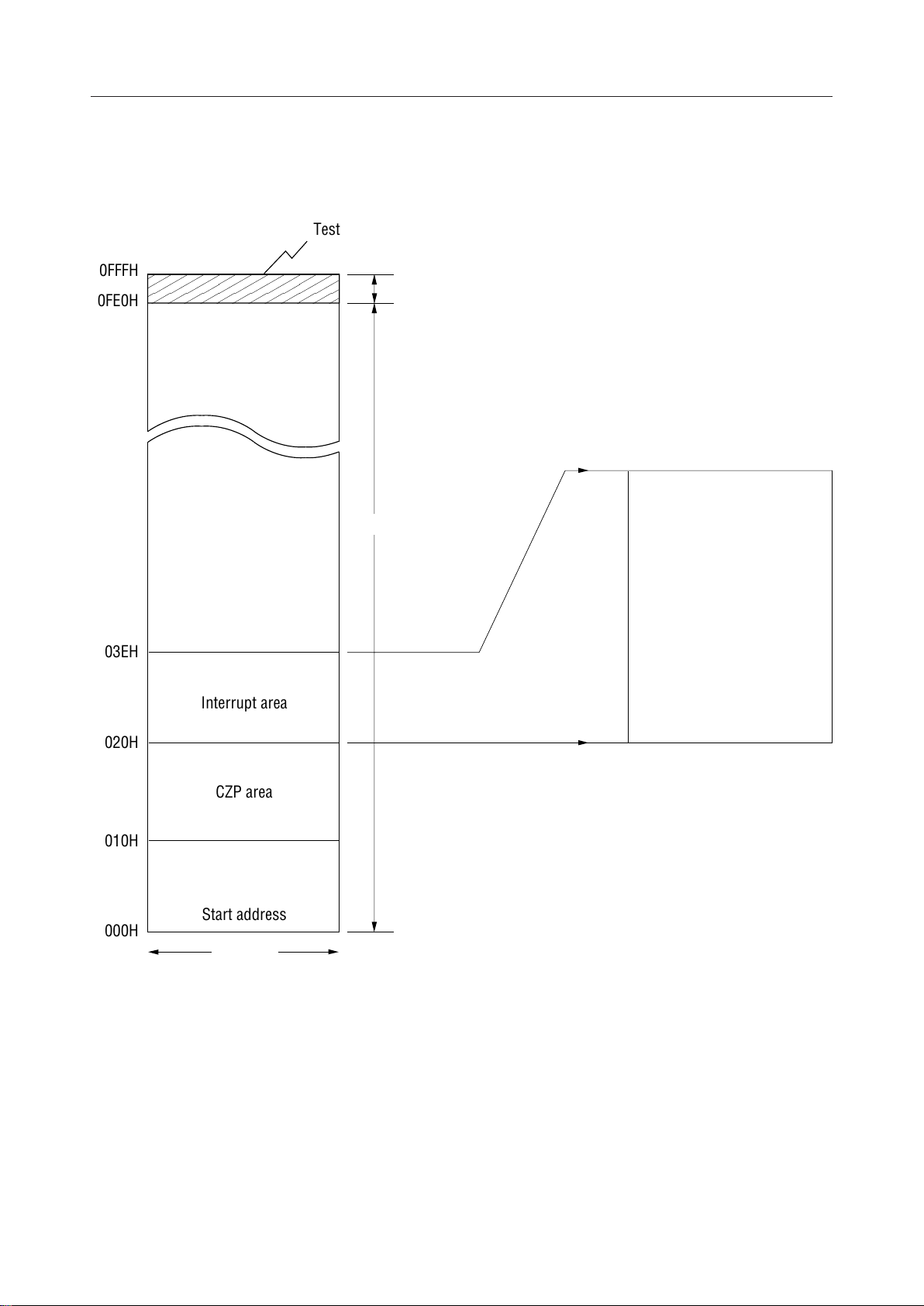
MEMORY MAPS
Program Memory
Test program area
0FFFH
0FE0H
03EH
020H
,,,,,,,,,,,
,,,,,,,,,,,
,,,,,,,,,,,
Interrupt area
32 bytes
4064 bytes
03BH
038H
035H
032H
02FH
02CH
029H
026H
023H
020H
Contents of interrupt area
Watchdog interrupt
External interrupt (0)
Serial port interrupt
External interrupt (1)
ADC interrupt
256 Hz interrupt
32 Hz interrupt
16 Hz interrupt
1 Hz interrupt
0.1 Hz interrupt
CZP area
010H
Start address
000H
8 bits
Program Memory Map
Address 000H is the instruction execution start address by the system reset.
The CZP area from address 010H to address 01FH is the start address for the CZP subroutine of
1-byte call instruction.
The start address of interrupt subroutine is assigned to the interrupt address from address 020H
to 03DH.
The user area has 4064 bytes of address 000H to address 0FDF. No program can be stored in the
test program area.
11/41
Page 12
¡ Semiconductor MSM64164C
Data Memory
The data memory area consists of 8 banks and each bank has 256 nibbles (256 ¥ 4 bits).
The data RAM is assigned to BANK 7 and peripheral ports are assigned to BANK 0.
7FFH
780H
700H
6FFH
BANK7
Data RAM area
(256 nibbles)
Inaccessible area
Data/Stack area (128 nibbles)
Contents of 000H to 07FH
07FH
SFR area
100H
0FFH
080H
07FH
000H
Unused area
BANK 0
000H
4 bits
Data Memory Map
Half the data RAM area (128 nibbles) is shared by the stack area. The stack is a memory starting
from address 7FFH toward the low-order addresses where 4 nibbles are used by Subroutine Call
Instruction and 8 nibbles are used by an interrupt.
The addresses 080H to 0FFH of BANK 0 are not assigned as the data memory, so access to these
addresses has no effect. Moreover, it is impossible to access BANK 1 to BANK 6.
12/41
Page 13
¡ Semiconductor MSM64164C
ABSOLUTE MAXIMUM RATINGS (1.5 V Spec.)
(V
= 0 V)
DD
Parameter Symbol Condition Rating Unit
Power Supply Voltage 1 V
Power Supply Voltage 2 V
Power Supply Voltage 3 V
Power Supply Voltage 4 V
Power Supply Voltage 5 V
Input Voltage 1 V
Input Voltage 2 V
Input Voltage 3 V
Output Voltage 1 V
Output Voltage 2 V
Output Voltage 3 V
Output Voltage 4 V
Output Voltage 5 V
Storage Temperature T
SS1
SS2
SS3
SSL
SS
IN1
IN2
IN3
OUT1
OUT2
OUT3
OUT4
OUT5
STG
Ta = 25°C –2.0 to +0.3 V
Ta = 25°C –4.0 to +0.3 V
Ta = 25°C –5.5 to +0.3 V
Ta = 25°C –2.0 to +0.3 V
Ta = 25°C –5.5 to +0.3 V
V
Input, Ta = 25°C V
SS1
V
Input, Ta = 25°C V
SS
V
Input, Ta = 25°C V
SSL
V
Output, Ta = 25°C V
SS1
V
Output, Ta = 25°C V
SS2
V
Output, Ta = 25°C V
SS3
V
Output, Ta = 25°C V
SS
V
Output, Ta = 25°C V
SSL
—
– 0.3 to +0.3 V
SS1
– 0.3 to +0.3 V
SS
– 0.3 to +0.3 V
SSL
– 0.3 to +0.3 V
SS1
– 0.3 to +0.3 V
SS2
– 0.3 to +0.3 V
SS3
– 0.3 to +0.3 V
SS
– 0.3 to +0.3 V
SSL
–55 to +150 °C
RECOMMENDED OPERATING CONDITIONS (1.5 V Spec.)
Parameter Symbol Condition Range Unit
Operating Temperature
Operating Voltage
External 400 kHz RC Oscillator
Resistance
Crystal Oscillation Frequency
T
op
V
SS1
V
SS
R
OS
f
XT
—
—
—
—
—
= 0 V)
(V
DD
–40 to +85 °C
–1.7 to –1.25 V
–5.25 to V
SS1
250 to 500 kW
30 to 35 kHz
V
13/41
Page 14

¡ Semiconductor MSM64164C
ELECTRICAL CHARACTERISTICS (1.5 V Spec.)
DC Characteristics
(VDD = 0 V, V
= VSS = –1.5 V, Ta = –40 to +85°C unless otherwise specified)
SS1
Parameter
V
Voltage V
SS2
Voltage V
V
SS3
Voltage V
V
SSL
Crystal Oscillation
Start Voltage
Crystal Oscillation
Hold Voltage
Crystal Oscillation
Stop Detection Time
Internal Crystal
Oscillator Capacitance
External Crystal
Oscillator Capacitance
Internal Crystal
Oscillator Capacitance
Internal 400k RC
Oscillator Capacitance
400k RC Oscillation
Frequency
POR Generation
Voltage
POR Non-generation
Voltage
Symbol
SS2Ca
SS3Ca
SSL
V
STA
V
HOLD
T
STOP
C
G
C
GEX
C
D
C
OS
f
OSC
V
POR1
V
POR2
Condition Min. Typ. Max. Unit
+100%
, Cb, C
= 0.1 mF –3.2 –3.0 –2.8 V
12
–50%
+100%
, Cb, C
= 0.1 mF –4.7 –4.5 –4.3 V
12
–50%
— –1.5 –1.3 –0.6 V
Oscillation start time:
within 5 seconds
— — –1.45 V
— — — –1.25 V
— 0.1 — 1000 ms
—101520pF
When external CG used 10 — 30 pF
—101520pF
— 8 12 16 pF
External resistor R
= –1.25 to –1.7 V
V
SS1
When V
is between V
SS1
and –1.5 V
No POR when V
and –1.5 V
V
POR2
= 300 kW
OS
is between
SS1
POR1
80 220 350 kHz
–0.4 — 0 V
–1.5 — –1.2 V
Measuring
Circuit
1
Notes: 1. "POR" denotes Power On Reset.
2. "T
" indicates that if the crystal oscillator stops over the value of T
STOP
system reset occurs.
STOP
, the
14/41
Page 15

¡ Semiconductor MSM64164C
DC Characteristics (continued)
Parameter
Symbol
Supply Current 1 I
Supply Current 2 I
Supply Current 3 I
Supply Current 4 I
Supply Current 5 I
(VDD = 0 V, V
SS1
Condition Min. Typ. Max. Unit
CPU in halt state
DD1
(400k RC oscillation halt)
CPU in operating state
DD2
(400k RC oscillation halt)
CPU in operating state
(400k RC oscillation in operation)
DD3
R
= 300 kW
OS
Serial transfer,
f
= 300 kHz,
SCK
DD4
CPU in operating state
(400k RC oscillaiton halt)
CPU in halt state
(400k RC oscillation
halt), RC oscillator for
DD5
A/D converter is in
operating state
= VSS = –1.5 V, Ta = –40 to +85°C unless otherwise specified)
Measuring
Circuit
Ta = –40 to +40°C
Ta = +40 to +85°C
Ta = –40 to +40°C
Ta = +40 to +85°C
—2 5mA
—230mA
—515mA
—540mA
—4080mA
Ta = –40 to +40°C
Ta = +40 to +85°C
RT0 = 10 kW
RT0 = 2 kW
—725mA
—750mA
— 150 230 mA
— 600 900 mA
1
15/41
Page 16

¡ Semiconductor MSM64164C
DC Characteristics (continued)
(V
DD
= 0 V, V
SS1
= V
= V
SSL
= –1.5 V, V
SS
= –3.0 V, V
SS2
Ta = –40 to +85°C unless otherwise specified)
= –4.5 V,
SS3
Parameter
(Pin Name)
Output Current 1
(P1.0)
Output Current 2
(P1.1 to P1.3)
(P2.0 to P2.3)
(P3.0 to P3.3)
(P4.0 to P4.3)
Output Current 3
(BD)
Output Current 4
(RT0, RT1, RS0, RS1,
CRT0, CS0, CS1)
Output Current 5
(When L26 to L33 are
configured as output
ports)
Symbol
I
OH1
I
OL1
I
OH1SVSS
I
OL1S
I
OH2
I
OL2
I
OH2SVSS
I
OL2S
I
OH3
I
OL3
I
OH4
I
OL4
I
OH5
I
OL5
I
OH5SVSS
I
OL5S
Condition Unit
V
= –0.5 V
OH1
V
= VSS + 0.5 V 1.0 3.0 9.0 mA
OL1
= –5 V, V
V
= –5 V, V
SS
= –0.5 V
V
OH2
V
= V
OL2
SS
= –5 V, V
V
= –5 V, V
SS
V
= –0.7 V –1.8 –0.6 –0.2 mA
OH3
V
= V
OL3
SS1
V
= –0.1 V –1.1 –0.6 –0.3 mA
OH4
V
= V
OL4
SS1
V
= –0.5 V –1.5 –0.5 –0.1 mA
OH5
V
= V
OL5
SS
= –5 V, V
V
= –5 V, V
SS
= –0.5 V –36 –12 –4.0 mA
OH1S
= V
OL1
+ 0.5 V 4.0 12 36 mA
SS
+ 0.5 V 0.2 0.7 2.1 mA
= –0.5 V –9.0 –3.0 –1.0 mA
OH2S
= V
OL2
+ 0.5 V 1.0 3.0 9.0 mA
SS
+ 0.7 V 0.2 0.6 1.8 mA
+ 0.1 V 0.3 0.6 1.1 mA
+ 0.5 V 0.1 0.5 1.5 mA
= –0.5 V –2.0 –0.7 –0.2 mA
OH5S
= V
OL5S
+ 0.5 V 0.2 0.7 2.0 mA
SS
Min. Typ. Max.
–2.1 –0.7 –0.2 mA
–2.1 –0.7 –0.2 mA
Measuring
Circuit
2
Output Current 6
(OSC2)
Output Current 7
(L0 to L33)
Output Leakage Current
(P1.0 to P1.3)
(P2.0 to P2.3)
(P3.0 to P3.3)
(P4.0 to P4.3)
(RT0, RT1, RS0, RS1,
CRT0, CS0, CS1)
I
OH6
I
I
OH7
I
OMH7VOMH7
I
OMH7SVOMH7S
I
OML7VOML7
I
OML7SVOML7S
I
I
OOH
I
OOL
OL6
OL7
V
V
V
V
V
V
OH6
OL6
OH7
OL7
OH
OL
= V
= V
= V
= –0.5 V –2.1 –0.7 –0.2 mA
= V
+ 0.5 V 0.2 0.7 2.1 mA
SS1
= –0.2 V
= V
SS1
= V
SS1
= V
SS2
= V
SS2
+ 0.2 V
SS3
DD
SS1
+ 0.2 V
– 0.2 V
+ 0.2 V
– 0.2 V
(VDD level)
(V
level)
SS1
level)
(V
SS1
(V
level)
SS2
(V
level)
SS2
(V
level)
SS3
— — –4.0 mA
4.0 — — mA
— — –4.0 mA
4.0 — — mA
— — –4.0 mA
4.0 — — mA
— — 0.3 mA
–0.3 — — mA
16/41
Page 17

¡ Semiconductor MSM64164C
DC Characteristics (continued)
Parameter
(Pin Name)
Input Current 1
(P0.0 to P0.3)
(P2.0 to P2.3)
(P3.0 to P3.3)
(P4.0 to P4.3)
Input Current 2
(IN0, IN1)
Input Current 3
(OSC1)
Symbol
I
IH1
I
IL1
I
IH1S
I
IL1S
I
IH1Z
I
IL1Z
I
IH2
I
IH2Z
I
IL2Z
I
IL3
I
IH3Z
I
IL3Z
(V
= 0 V, V
DD
SS1
= V
SSL
= V
= –1.5 V, V
SS
= –3.0 V, V
SS2
= –4.5 V,
SS3
Ta = –40 to +85°C unless otherwise specified)
Condition Unit
V
= V
IH1
V
IL1
V
= V
IH1
V
IL1
V
IH1
V
IL1
V
IH2
V
IH2
V
IL2
V
IL3
V
IH3
V
IL3
(when pulled down)
DD
= V
(when pulled up) –60 –18 –5.0 mA
SS
, V
= –5 V (when pulled down)
DD
SS
= V
= –5 V (when pulled up)
SS
= V
(in a high impedance state)
DD
= V
(in a high impedance state)
SS
= V
(when pulled down) 5.0 18 60 mA
DD
(in a high impedance state)
= V
DD
= V
(in a high impedance state)
SS1
= V
(when pulled up) –60 –22 –6.0 mA
SS1
= V
(in a high impedance state)
DD
= V
(in a high impedance state)
SS1
Min. Typ. Max.
5.0 18 60 mA
70 250 660 mA
–660 –250 –70 mA
0 — 1.0 mA
–1.0 — 0 mA
0 — 1.0 mA
–1.0 — 0 mA
0 — 1.0 mA
–1.0 — 0 mA
Measuring
Circuit
3
Input Current 4
(RESET, TST1, TST2)
Input Voltage 1
(P0.0 to P0.3)
(P2.0 to P2.3)
(P3.0 to P3.3)
(P4.0 to P4.3)
Input Voltage 2
(IN0, IN1, OSC1)
Input Voltage 3
(RESET, TST1, TST2)
V
V
I
I
V
V
IH1S
V
V
V
V
IH4
IL4
IH1
IL1
IL1S
IH2
IL2
IH3
IL3
V
V
V
V
IH4
IL4
SS
SS
= V
DD
= V
SS1
= –5 V
= –5 V
0 — 1.0 mA
–1.5 –0.75 –0.3 mA
— –0.3 — 0 V
— –1.5 — –1.2 V
–1.0 — 0 V
–5.0 — –4.0 V
4
— –0.3 — 0 V
— –1.5 — –1.2 V
— –0.3 — 0 V
— –1.5 — –1.2 V
17/41
Page 18

¡ Semiconductor MSM64164C
DC Characteristics (continued)
(V
DD
= 0 V, V
SS1
= V
= V
SSL
= –1.5 V, V
SS
= –3.0 V, V
SS2
= –4.5 V,
SS3
Ta = –40 to +85°C unless otherwise specified)
Parameter
(Pin Name)
Hysteresis Width
(P0.0 to P0.3)
(P2.0 to P2.3)
(P3.0 to P3.3)
(P4.0 to P4.3)
Hysteresis Width
(RESET, TST1, TST2)
Input Pin Capacitance
(P0.0 to P0.3)
(P2.0 to P2.3)
(P3.0 to P3.3)
(P4.0 to P4.3)
Symbol
DV
T1
DV
T1S
DV
T2
C
IN
V
SS
Condition Unit
Min. Typ. Max.
— 0.05 0.1 0.3 V
= –5 V
0.25 1.0 1.5 V
— 0.05 0.1 0.3 V
— — — 5.0 pF
Measuring
Circuit
4
1
18/41
Page 19

¡ Semiconductor MSM64164C
Measuring circuit 1
CS0
RT0 RI0
R
OS
C
l
V
Measuring circuit 2
OSC1
OSC2
V
SSL
RT0 CS0 IN0
XT
Crystal
32.768 kHz
XT
C1
C
12
C2
V
DD
V
SS1
V
SS2
A
C
a
V
SS3
C
b
V V
V
SS
Ca, Cb, C12, C
R
OS
RT0
CS0
RI0
: 0.1 mF
l
: 300 kW
: 10 kW/2 kW
: 820 pF
: 10 kW
(*2)
V
IH
(*1)
OUTPUT
A
INPUT
V
IL
V
DD
V
SS1
V
SS2
V
SS3
V
SSL
V
SS
19/41
Page 20

¡ Semiconductor MSM64164C
Measuring circuit 3
(*3)
A
Measuring circuit 4
V
IH
(*3)
V
IL
INPUT
INPUT
OUTPUT
V
DD
V
SS1
V
SS2VSS3
V
SSL
V
SS
Waveform
OUTPUT
Monitoring
DD
V
V
SS1
V
SS2VSS3
V
SSL
V
*1 Input logic circuit to determine the specified measuring conditions.
*2 Measured at the specified output pins.
*3 Measured at the specified input pins.
SS
20/41
Page 21

¡ Semiconductor MSM64164C
(
)
A/D Converter Characteristics
= 0 V, V
(V
DD
Parameter Symbol Condition
RS0, RS1,
Resistor
for Oscillation
RT0,
RT0-1,
CS0, CT0, CS1 ≥ 740 pF
RT1
Input Current
Limiting Resistor
Oscillation
Frequency
RI0, RI1
f
OSC1
f
OSC2
f
OSC3
Kf1
Resistor for oscillation = 2 kW
Resistor for oscillation = 10 kW
Resistor for oscillation = 200 kW
RT0, RT0-1, RT1 = 2 kW
RS•RT Oscillation
Frequency Ratio
(*)
Kf2
Kf3
RT0, RT0-1, RT1 = 10 kW
RT0, RT0-1, RT1 = 200 kW
SS1
—
= V
= –1.5 V, Ta = –40 to +85°C unless otherwise specified)
SS
Min. Typ. Max.
2.0
1.0
165
41.8
2.55
3.89
0.990
0.0561
——
10
221
52.2
3.04
4.18
1.0
0.0584
—
256
60.6
3.53
4.35
1.010
0.0637
Unit
kW
kW
kHz
kHz
kHz
—
—
—
Measur-
ing
Circuit
5
* Kfx is the ratio of the oscillation frequency by a sensor resistor to the oscillation frequency
by a reference resistor in the same condition.
Kfx =
(RT0–CS0 Oscillation)
f
OSCX
f
(RS0–CS0 Oscillation)
OSCX
x = 1, 2, 3
f
(RT0-1–CS0 Oscillation)
OSCX
,,
f
(RS0–CS0 Oscillation)
OSCX
f
(RT1–CS1 Oscillation)
OSCX
f
(RS1–CS1 Oscillation)
OSCX
21/41
Page 22

¡ Semiconductor MSM64164C
Measuring circuit 5
(CROSC1) (CROSC0)
RT1
RS1
CS1
RI1
RT1 RS1 CS1 IN1 IN0 CS0 RS0 CRT0 RT0
RESET
TST1
TST2
P0.0
D. U. T.
P0.1
P0.2
RI0
CS0
RS0
CT0
RT0-1
P4.3
RT0
Frequency
Measurement
(f
)
OSCX
Oscillation Mode Designation
P0.3
V
DD
RT0, RT0-1, RT1 = 2 kW/10 kW/200 kW
RS0, RS1 = 10 kW
RI0, RI1 = 10 kW
CS0, CT0, CS1 = 820 pF
C
= 0.1 mF
l
V
SSL
V
C
l
SS
V
SS1
22/41
Page 23

¡ Semiconductor MSM64164C
AC Characteristics (Serial Interface)
(V
Parameter Symbol Condition Unit
SCLK Input Fall Time
SCLK Input Rise Time
SCLK Input "L" Level Pulse Width
SCLK Input "H" Level Pulse Width
SCLK Input Cycle Time
SCLK Output Cycle Time
SCLK Output Cycle Time
SOUT Output Delay Time
SIN Input Setup Time
SIN Input Hold TIme
SCLK
(P4.2)
t
f
t
r
t
CWL
t
CWH
t
CYC
t
CYC1(O)
t
CYC2(O)
t
DDR
t
DS
t
DH
t
CYC
= 0 V, V
DD
—
—
—
—
= –5.25 V to V
V
SS
SS1
CPU is operating at 32.768 kHz.
CPU is operating at 400 kHz.
= 10 pF
C
l
—
—
= –1.5 V, V
SS1
= –5 V, Ta = –40 to +85°C)
SS
Max.Typ.Min.
— — 1.0
— — 1.0
0.8 — —
0.8
2.0
—
—
—
0.5 —
—
—
30.5
2.5
—
—
0.8 — —
ms
ms
ms
ms—
ms—
ms—
ms—
ms0.4
ms
ms
0 V
t
DDR
SOUT
(P4.0)
SIN
(P3.3)
("H" level = –1 V, "L" level = –4 V)
t
r
t
CWH
t
DDR
t
f
t
CWL
0 V
t
DS
t
DH
t
DS
0 V
23/41
Page 24

¡ Semiconductor MSM64164C
ABSOLUTE MAXIMUM RATINGS (3.0 V Spec.)
(V
= 0 V)
DD
Parameter Symbol Condition Rating Unit
Power Supply Voltage 1 V
Power Supply Voltage 2 V
Power Supply Voltage 3 V
Power Supply Voltage 4 V
Power Supply Voltage 5 V
Input Voltage 1 V
Input Voltage 2 V
Input Voltage 3 V
Output Voltage 1 V
Output Voltage 2 V
Output Voltage 3 V
Output Voltage 4 V
Storage Temperature T
SS1
SS2
SS3
SSL
SS
IN1
IN2
IN3
OUT1
OUT2
OUT3
OUT4
STG
Ta = 25°C –2.0 to +0.3 V
Ta = 25°C –4.0 to +0.3 V
Ta = 25°C –5.5 to +0.3 V
Ta = 25°C –4.0 to +0.3 V
Ta = 25°C –5.5 to +0.3 V
V
Input, Ta = 25°C V
SS2
– 0.3 to +0.3 V
SS2
VSS Input, Ta = 25°C VSS – 0.3 to +0.3 V
V
Input, Ta = 25°C V
SSL
V
Output, Ta = 25°C V
SS2
V
Output, Ta = 25°C V
SS3
– 0.3 to +0.3 V
SSL
– 0.3 to +0.3 V
SS2
– 0.3 to +0.3 V
SS3
VSS Output, Ta = 25°C VSS – 0.3 to +0.3 V
V
Output, Ta = 25°C V
SSL
– 0.3 to +0.3 V
SSL
— –55 to +150 °C
RECOMMENDED OPERATING CONDITIONS (3.0 V Spec.)
Parameter Symbol Condition Range Unit
Operating Temperature T
op
Using LCD driver with
"duty 1/2"
V
Operating Voltage
V
SS2
SS
Except using LCD driver
with "duty 1/2"
External 400 kHz RC Oscillator
R
Resistance
Crystal Oscillation Frequency f
OS
XT
* Indicates that the value of VSS is 80% of V
— –40 to +85 °C
—
(0.8•V
— 90 to 500 k
— 30 to 66 kHz
and should not exceed –2.0 V.
SS2
(V
= 0 V)
DD
–3.5 to –2.2
–3.5 to –2.0 V
–5.25 to
, –2.0 max.)*
SS2
W
24/41
Page 25

¡ Semiconductor MSM64164C
ELECTRICAL CHARACTERISTICS (3.0 V Spec.)
DC Characteristics
Parameter
V
Voltage V
SS1
Voltage V
V
SS3
Voltage V
V
SSL
Crystal Oscillation
Start Voltage
Crystal Oscillation
Hold Voltage
Crystal Oscillation
Stop Detection Time
Internal Crystal
Oscillator Capacitance
External Crystal
Oscillator Capacitance
Internal Crystal
Oscillator Capacitance
Internal 400k RC
Oscillator Capacitance
400k RC Oscillation
Frequency
POR Generation
Voltage
POR Non-generation
Voltage
Symbol
SS1Ca
SS3Ca
SSL
V
STA
V
HOLD
T
STOP
C
G
C
GEX
C
D
C
OS
f
OSC
V
POR1
V
POR2
(V
DD
= 0 V, V
SS2
= V
= –3.0 V, Ta = –40 to +85°C unless otherwise specified)
SS
Condition Min. Typ. Max. Unit
+100%
, Cb, C
= 0.1 mF –1.7 –1.5 –1.3 V
12
–50%
+100%
, Cb, C
= 0.1 mF –4.7 –4.5 –4.3 V
12
–50%
— –1.9 –1.3 –0.6 V
Oscillation start time:
within 5 seconds
— — –2.0 V
— — — –2.0 V
— 0.1 — 1000 ms
— 101520pF
When external CG used 10 — 30 pF
— 101520pF
— 8.0 12 16 pF
External resistor R
= –2.0 to –3.5 V
V
SS2
When V
is between V
SS2
and –3.0 V
No POR when V
and –3.0 V
V
POR2
= 100 k
OS
is between
SS2
POR1
W
300 400 620 kHz
–0.7 — 0 V
–3.0 — –2.0 V
Measuring
Circuit
1
Notes: 1. "POR" denotes Power On Reset.
2. "T
" indicates that if the crystal oscillator stops over the value of T
STOP
system reset occurs.
STOP
, the
25/41
Page 26

¡ Semiconductor MSM64164C
DC Characteristics (continued)
(VDD = 0 V, V
= VSS = –3.0 V, Ta = –40 to +85°C unless otherwise specified)
SS2
Parameter Symbol Condition Min. Typ. Max. Unit
Supply Current 1 I
Supply Current 2 I
CPU in halt state
DD1
(400k RC oscillation halt)
CPU in operating state
DD2
(400k RC oscillation halt)
Ta = –40 to +40°C
Ta = +40 to +85°C
Ta = –40 to +40°C
Ta = +40 to +85°C
— 1.5 4.5 mA
— 1.5 30 mA
— 5.0 15 mA
— 5.0 40 mA
CPU in operating state
Supply Current 3 I
Supply Current 4 I
Supply Current 5 I
DD3
(400k RC oscillation in operation)
Serial transfer,
f
= 300 kHz,
DD4
DD5
SCK
CPU in operating state
(400k RC oscillation halt)
CPU in halt state
(400k RC oscillation
halt), RC oscillator for
A/D converter is in
operating state
Ta = –40 to +40°C
Ta = +40 to +85°C
RT0 = 10 kW
RT0 = 2 kW
— 220 450 mA
— 7.0 25 mA
— 7.0 50 mA
— 300 450 mA
— 1300 2000 mA
Measuring
Circuit
1
26/41
Page 27

¡ Semiconductor MSM64164C
DC Characteristics (continued)
(V
DD
= 0 V, V
SS1
= V
= –1.5 V, V
SSL
SS2
= V
= –3.0 V, V
SS
Ta = –40 to +85°C unless otherwise specified)
= –4.5 V,
SS3
Parameter
(Pin Name)
Output Current 1
(P1.0)
Output Current 2
(P1.1 to P1.3)
(P2.0 to P2.3)
(P3.0 to P3.3)
(P4.0 to P4.3)
Output Current 3
(BD)
Output Current 4
(RT0, RT1, RS0, RS1,
CRT0, CS0, CS1)
Symbol Condition Unit
I
OH1
I
I
OH1SVSS
I
OL1S
I
OH2
I
I
OH2SVSS
I
OL2S
I
OH3
I
I
OH4
I
OL1
OL2
OL3
OL4
V
= –0.5 V
OH1
V
= V
+ 0.5 V 3.0 8.0 25 mA
SS
= –5 V, V
= –5 V, V
= –0.5 V –36 –12 –4 mA
OH1S
= V
OL1
+ 0.5 V 4.0 12 36 mA
SS
= –0.5 V
= V
+ 0.5 V 0.7 2.0 6.0 mA
SS
= –5 V, V
= –5 V, V
= –0.5 V –9.0 –3.0 –1.0 mA
OH2S
= V
OL2
+ 0.5 V 1.0 3.0 9.0 mA
SS
= –0.7 V –6.0 –2.0 –0.7 mA
= V
+ 0.7 V 0.7 2.0 6.0 mA
SS2
= –0.1 V –2.5 –1.3 –0.7 mA
= V
+ 0.1 V 0.7 1.3 2.5 mA
SS2
V
V
V
V
V
V
V
V
OL1
SS
OH2
OL2
SS
OH3
OL3
OH4
OL4
Min. Typ. Max.
–6 –2 –0.7 mA
–6.0 –2.0 –0.7 mA
Measuring
Circuit
Output Current 5
(When L26 to L33 are
configured as output
ports)
Output Current 6
(OSC2)
Output Current 7
(L0 to L33)
Output Leakage Current
(P1.0 to P1.3)
(P2.0 to P2.3)
(P3.0 to P3.3)
(P4.0 to P4.3)
(RT0, RT1, RS0, RS1,
CRT0, CS0, CS1)
I
OH5
I
I
OH5SVSS
I
OL5S
I
OH6
I
I
OH7
I
OMH7VOMH7
I
OMH7SVOMH7S
I
OML7VOML7
I
OML7SVOML7S
I
I
OOH
I
OOL
OL5
OL6
OL7
V
V
V
V
V
V
V
V
V
OH5
OL5
SS
OH6
OL6
OH7
OL7
OH
OL
= –5 V, V
= –5 V, V
= V
= V
= V
= –0.5 V –1.5 –0.6 –0.15 mA
= V
+ 0.5 V 0.15 0.6 1.5 mA
SS
= –0.5 V –2.0 –0.7 –0.2 mA
OH5S
= V
OL5S
+ 0.5 V 0.2 0.7 2.0 mA
SS
= –0.5 V –6.0 –2.0 –0.7 mA
= V
+ 0.5 V 0.7 2.0 6.0 mA
SS2
= –0.2 V
= V
SS1
= V
SS1
= V
SS2
= V
SS2
+ 0.2 V
SS3
DD
SS2
+ 0.2 V
– 0.2 V
+ 0.2 V
– 0.2 V
(VDD level)
(V
level)
SS1
(V
level)
SS1
(V
level)
SS2
(V
level)
SS2
(V
level)
SS3
— — –4.0 mA
4.0 — — mA
— — –4.0 mA
4.0 — — mA
— — –4.0 mA
4.0 — — mA
— — 0.3 mA
–0.3 — — mA
2
27/41
Page 28

¡ Semiconductor MSM64164C
DC Characteristics (continued)
(V
DD
= 0 V, V
SS1
= V
= –1.5 V, V
SSL
SS2
= V
= –3.0 V, V
SS
Ta = –40 to +85°C unless otherwise specified)
= –4.5 V,
SS3
Parameter
(Pin Name)
Input Current 1
(P0.0 to P0.3)
(P2.0 to P2.3)
(P3.0 to P3.3)
(P4.0 to P4.3)
Input Current 2
(IN0, IN1)
Input Current 3
(OSC1)
Symbol Condition Unit
I
I
I
IH1S
I
IL1S
I
IH1ZVIH1
I
IL1Z
I
I
IH2ZVIH2
I
IL2Z
I
I
IH3ZVIH3
I
IL3Z
IH1
IL1
IH2
IL3
V
V
V
V
V
V
V
V
V
IH1
IL1
IH1
IL1
IL1
IH2
IL2
IL3
IL3
= V
(when pulled down)
DD
= V
(when pulled up) –300 –90 –30 mA
SS
, V
= V
= V
= V
= V
= V
= V
= V
= V
= –5 V (when pulled down)
DD
SS
= –5 V (when pulled up)
SS
(in a high impedance state)
DD
(in a high impedance state)
SS
= V
(when pulled down) 30 90 300 mA
DD
(in a high impedance state)
DD
(in a high impedance state)
SS2
= V
(when pulled up) –300 –110 –10 mA
SS2
(in a high impedance state)
DD
(in a high impedance state)
SS2
Min. Typ. Max.
30 90 300 mA
80 250 800 mA
–800 –250 –80 mA
0 — 1.0 mA
–1.0 — 0 mA
0 — 1.0 mA
–1.0 — 0 mA
0 — 1.0 mA
–1.0 — 0 mA
Measuring
Circuit
3
Input Current 4
(RESET, TST1, TST2)
Input Voltage 1
(P0.0 to P0.3)
(P2.0 to P2.3)
(P3.0 to P3.3)
(P4.0 to P4.3)
Input Voltage 2
(IN0, IN1, OSC1)
Input Voltage 3
(RESET, TST1, TST2)
V
V
I
IH4
I
IL4
V
V
IH1S
IL1S
V
V
V
V
IH1
IL1
IH2
IL2
IH3
IL3
V
V
V
V
IH4
IL4
SS
SS
= V
DD
= V
SS2
= –5 V
= –5 V
0 — 1.0 mA
–3.0 –1.5 –0.75 mA
— –0.6 — 0 V
— –3.0 — –2.4 V
–1.0 — 0 V
–5.0 — –4.0 V
4
— –0.6 — 0 V
— –3.0 — –2.4 V
— –0.6 — 0 V
— –3.0 — –2.4 V
28/41
Page 29

¡ Semiconductor MSM64164C
DC Characteristics (continued)
Parameter
(Pin Name)
Hysteresis Width
(P0.0 to P0.3)
(P2.0 to P2.3)
(P3.0 to P3.3)
(P4.0 to P4.3)
Hysteresis Width
(RESET, TST1, TST2)
Input Pin Capacitance
(P0.0 to P0.3)
(P2.0 to P2.3)
(P3.0 to P3.3)
(P4.0 to P4.3)
Symbol
DV
T1
DV
T1S
DV
T2
C
IN
V
SS
(V
= 0 V, V
DD
SS1
= V
= –1.5 V, V
SSL
SS2
Ta = –40 to +85°C unless otherwise specified)
Condition Unit
Min. Typ. Max.
— 0.2 0.5 1.0 V
= –5 V
0.25 1.0 1.5 V
— 0.2 0.5 1.0 V
— — — 5.0 pF
= V
= –3.0 V, V
SS
= –4.5 V,
SS3
Measuring
Circuit
4
1
29/41
Page 30

¡ Semiconductor MSM64164C
Measuring circuit 1
CS0
RT0 RI0
R
OS
C
l
V
Measuring circuit 2
OSC1
OSC2
V
SSL
RT0 CS0 IN0
XT
Crystal
32.768 kHz
XT
C1
C
12
C2
V
DD
V
SS2
V
SS1
A
C
a
V
SS3
C
b
V V
V
SS
C
l
Ca, Cb, C
R
OS
RT0
CS0
RI0
12
: 0.47 mF
: 0.1 mF
: 100 kW
: 10 kW/2 kW
: 820 pF
: 10 kW
(*2)
V
IH
(*1)
OUTPUT
A
INPUT
V
IL
V
DD
V
SS1
V
SS2
V
SS3
V
SSL
V
SS
30/41
Page 31

¡ Semiconductor MSM64164C
Measuring circuit 3
(*3)
A
Measuring circuit 4
V
IH
(*3)
V
IL
INPUT
V
INPUT
DD
OUTPUT
V
SS1
V
SS2VSS3
V
SSL
V
SS
Waveform
OUTPUT
Monitoring
V
DD
V
SS1
V
SS2
V
SS3
V
SSL
V
SS
*1 Input logic circuit to determine the specified measuring conditions.
*2 Measured at the specified output pins.
*3 Measured at the specified input pins.
31/41
Page 32

¡ Semiconductor MSM64164C
(
)
A/D Converter Characteristics
(V
= 0 V, V
DD
SS2
= V
= –3.0 V, Ta = –40 to +85°C unless otherwise specified)
SS
Parameter Symbol Condition
Min. Typ. Max.
Unit
Measur-
ing
Circuit
RS0, RS1,
Resistor
for Oscillation
RT0,
RT0-1,
CS0, CT0, CS1 ≥ 740 pF
1.0
——
kW
RT1
Input Current
Limiting Resistor
RI0, RI1
—
1.0
10
—
kW
5
Oscillation
Frequency
f
OSC1
f
OSC2
f
OSC3
Kf1
Resistor for oscillation = 2 kW
Resistor for oscillation = 10 kW
Resistor for oscillation = 200 kW
RT0, RT0-1, RT1 = 2 kW
200
46.5
2.79
4.115
239
55.4
3.32
4.22
277
64.3
3.85
4.326
kHz
kHz
kHz
—
RS•RT Oscillation
Frequency Ratio
(*)
Kf2
Kf3
RT0, RT0-1, RT1 = 10 kW
RT0, RT0-1, RT1 = 200 kW
0.990
0.0573
1.0
0.0616
1.010
0.0659
—
—
* Kfx is the ratio of the oscillation frequency by a sensor resistor to the oscillation frequency
by a reference resistor in the same condition.
Kfx =
f
(RT0–CS0 Oscillation)
OSCX
f
(RS0–CS0 Oscillation)
OSCX
x = 1, 2, 3
f
(RT0-1–CS0 Oscillation)
OSCX
,,
(RS0–CS0 Oscillation)
f
OSCX
f
(RT1–CS1 Oscillation)
OSCX
(RS1–CS1 Oscillation)
f
OSCX
32/41
Page 33

¡ Semiconductor MSM64164C
Measuring circuit 5
(CROSC1) (CROSC0)
RT1
RS1
CS1
RI1
RT1 RS1 CS1 IN1 IN0 CS0 RS0 CRT0 RT0
RESET
TST1
TST2
P0.0
D. U. T.
P0.1
RI0
CS0
RS0
CT0
RT0-1
P4.3
RT0
Frequency
Measurement
(f
)
OSCX
P0.2
Oscillation Mode Designation
P0.3
V
DD
RT0, RT0-1, RT1 = 2 kW/10 kW/200 kW
RS0, RS1 = 10 kW
RI0, RI1 = 10 kW
CS0, CT0, CS1 = 820 pF
C
= 0.47 mF
l
V
SSL
V
C
l
SS
V
SS2
33/41
Page 34

¡ Semiconductor MSM64164C
AC Characteristics (Serial Interface)
(V
Parameter Symbol Condition Unit
SCLK Input Fall Time
SCLK Input Rise Time
SCLK Input "L" Level Pulse Width
SCLK Input "H" Level Pulse Width
SCLK Input Cycle Time
SCLK Output Cycle Time
SCLK Output Cycle Time
SOUT Output Delay Time
SIN Input Setup Time
SIN Input Hold TIme
SCLK
(P4.2)
t
f
t
r
t
CWL
t
CWH
t
CYC
t
CYC1(O)
t
CYC2(O)
t
DDR
t
DS
t
DH
t
CYC
= 0 V, V
DD
—
—
—
—
—
CPU is operating at 32.768 kHz.
CPU is operating at 400 kHz.
= 10 pF
C
l
—
—
SS2
= –3 V, V
= –5 V, Ta = –40 to +85°C)
SS
Max.Typ.Min.
— — 1.0
— — 1.0
0.8 — —
0.8
2.0
—
—
—
0.5 —
—
—
30.5
2.5
—
—
0.8 — —
ms
ms
ms
ms—
ms—
ms—
ms—
ms0.4
ms
ms
0 V
t
DDR
SOUT
(P4.0)
SIN
(P3.3)
("H" level = –1 V, "L" level = –4 V)
t
r
t
CWH
t
DDR
t
f
t
CWL
0 V
t
DS
t
DH
t
DS
0 V
34/41
Page 35

¡ Semiconductor MSM64164C
FUNCTIONAL DESCRIPTION
• A/D converter (ADC)
The MSM64164C has a built-in 2-channel RC oscillation type A/D converter. The A/D converter
is composed of a 2-channel oscillation circuit, Counter A (CNTA0-4, a 4.8-digit decade counter),
Counter B (CNTB0-3, a 14-bit binary counter), and A/D Converter Control Registers 0 and 1
(ADCON0, ADCON1).
By counting oscillation frequencies that vary depending on a resistor or capacitor connected to
the RC oscillation circuit, the A/D converter converts resistance values or capacitance values to
corresponding digital values. By using a thermistor or humidity sensor as a resistance, a
thermometer or a hygrometer can be constructed. By applying a separate sensor to each channel
of the 2-channel RC oscillation circuit, it is also possible to extend measure ranges or measure at
two places.
• Serial port (SIOP)
The MSM64164C has an 8-bit synchronous serial port. Receive/transmit operation of the serial
port is performed simultaneously and the serial transfer clock can select either internal or
external mode. Direction of transfer data can be big endian or little endian. Each pin of the serial
port is assigned as secondary functions of P3.3 and P4.0 to P4.2. Setting each bit of SIN, SOUT,
SPR and SCLK of P33CON and P40CON to P42CON to "1" makes each pin valid.
• LCD driver (LCD)
The MSM64164C has a built-in LCD driver for 34 outputs.
The LCD driver consists of 31 ¥ 4-bit display registers (DSPR0-30), the Display Control Register
(DSPCON), a 34-output LCD driver circuit, and a bias generation circuit (BIAS).
There are three types of driving methods: 1/4 duty, 1/3 duty and 1/2 duty. Software selects the
duty mode.
A mask option can select either a common driver or a segment driver for each LCD driver pin.
A mask option can also specify assignment of each bit of the display register to each segment.
All the display registers must be selected by a mask option.
L26 to L33 of the LCD driver can be configured to be output ports by a mask option.
The relationship between the duty, the bias method, and the maximum segment number follows:
1/4 duty 1/3 bias method ------- 120 segments
1/3 duty 1/3 bias method ------- 93 segments
1/2 duty 1/2 bias method ------- 64 segments
• Buzzer driver (BD)
The MSM64164C has a built-in buzzer driver with 15 buzzer output frequencies and 4 buzzer
output modes. Each buzzer output is selected by the Buzzer Control Register (BDCON) and the
Buzzer Frequency Control Register (BFCON).
• Capture circuit (CAPR)
The MSM64164C captures 32 Hz to 256 Hz output of the time base counter at the falling of Port
0.0 or 0.1 (P0.0 or P0.1) to "L" level when the pull-up resistor input is chosen, or at the rising to
"H" level when the pull-down resistor input is chosen. The capture circuit is composed of the
Capture Control Register (CAPCON) and the Capture Registers (CAPR0, CAPR1) that fetch
output from the time base counter.
35/41
Page 36

¡ Semiconductor MSM64164C
• Watchdog timer (WDT)
The MSM64164C has a built-in watchdog timer to detect CPU malfunction. The watchdog timer
is composed of a 6-bit watchdog timer counter (WDTC) to count a 16 Hz output and a watchdog
timer control register (WDTCON) to reset WDTC.
• Clock generation circuit (2CLK)
The clock generation circuit (2CLK) in the MSM64164C contains a 32.768 kHz crystal oscillation
circuit, a 400 kHz RC oscillation circuit, and a clock control port. This circuit generates the system
clock (CLK) and the time base clock (32.768 kHz).
The system clock drives the CPU while the time base clock drives the time base counter and the
buzzer driver.
Via the contents of the frequency Control Register (FCON), the system clock can be switched
between 32.768 kHz (the output of the crystal oscillation circuit) and 400 kHz (the output of the
RC oscillation circuit).
Note: The oscillation frequency of the RC oscillation circuit varies depending on the value of
an external resistor (ROS), operating power supply voltage (VDD), and ambient
temperatures (Ta).
• Time base counter (TBC)
The MSM64164C has a built-in time base counter (TBC) that generates clocks to be supplied to
internal peripheral circuits. The time base counter is composed of 15 binary counters and a 1/
10 frequency dividing circuit. The count clock of the time base is driven by the oscillation clock
(32.768 kHz) of the crystal oscillation circuit. The output of the time base counter is used for the
buzzer driver, the system reset circuit, the watchdog timer, the time base interrupt, the sampling
clocks of each port, and the capture circuit.
• I/O port
Input-output ports (P2, P3, P4) (12 bits) : Pull-up (pull-down) resistor input or high-
impedance input, CMOS output or NMOS
open drain output: these can be specified for
each bit; external 0 interrupt
Input port (P0) (4 bits) : Pull-up (pull-down) resistor input or high-
impedance input; external 1 interrupt
Output port (P1) (4 bits) : CMOS output or NMOS open drain output
• Interrupt (INTC)
The MSM64164C has ten interrupt sources (10 vector addresses), of which two are external
interrupts from ports and eight are internal interrupts.
Of the ten interrupt sources, only the watchdog interrupt cannot be disabled (non-maskable
interrupt). The other nine interrupts are controlled by the master interrupt enable flag (MI) and
the interrupt enable registers (IE0, IE1 and IE2). When an interrupt condition is met, the CPU
branches to a vector address corresponding to the interrupt source.
36/41
Page 37

37/41
¡ Semiconductor MSM64164C
APPLICATION CIRCUITS
3.0 V Spec. Application Circuit
RT1 RS1 CS1 RI1
L33 L0OSC2
OSC1
XT
XT
RESET
P1.0
P1.1
P1.2
P1.3
P0.0
P0.1
P0.2
P0.3
TST1
TST2
V
SSL
V
SS1
V
SS2
V
SS3
C1
C2
V
DD
3 V
C2
C
12
C
b
C
a
C
l
R
OS
Crystal
32.768 kHz
C
GEX
RI0
RT0
Buzzer
OSC monitor
IN0
CS0
RS0
CRT0
RT0
IN1
CS1
RS1
RT1
BD
P4.3
P4.2
MSM64164C-xxx
(3.0 V spec.)
L C D
CS0
RS0
• With 5 V interface
• Temperature
measurement
by two thermistors
• C
GEX
of crystal
oscillator : External
Switch matrix (4 ¥ 4)
V
SS
5 V
C
S
P4.1
P4.0
P3.3
SCLK
SPR
SOUT
SIN
To serial communication
interface (to 5 V (V
SS
) system)
Page 38

38/41
¡ Semiconductor MSM64164C
APPLICATION CIRCUITS (continued)
1.5 V Spec. Application Circuit
L33 L0
OSC2
OSC1
XT
XT
RESET
P1.0
P1.1
P1.2
P1.3
P0.0
P0.1
P0.2
P0.3
TST1
TST2
V
SSL
V
SS1
V
SS2
V
SS3
C1
C2
V
DD
1.5 V
C1
C
12
C
b
C
l
R
OS
Crystal
32.768 kHz
Switch matrix (4 ¥ 4)
RT1 RS1 CS1 RI1
RS0
RT0
Buzzer
IN0
CS0
RS0
CRT0
RT0
IN1
CS1
RS1
RT1
BD
P4.3
MSM64164C-xxx
(1.5 V spec.)
L C D
C
a
RI0
CS0
• Without 5 V interface
• Temperature
measurement
by two thermistors
• C
G
of crystal oscillator :
Internal
V
SS
P4.2
P4.1
P4.0
P3.3
Page 39

¡ Semiconductor MSM64164C
PACKAGE DIMENSIONS
(Unit : mm)
QFP80-P-1420-0.80-BK
Mirror finish
Package material
Lead frame material
Pin treatment
Solder plate thickness
Package weight (g)
Epoxy resin
42 alloy
Solder plating
5 mm or more
1.27 TYP.
Notes for Mounting the Surface Mount Type Package
The SOP, QFP, TSOP, SOJ, QFJ (PLCC), SHP and BGA are surface mount type packages, which
are very susceptible to heat in reflow mounting and humidity absorbed in storage.
Therefore, before you perform reflow mounting, contact Oki’s responsible sales person for the
product name, package name, pin number, package code and desired mounting conditions
(reflow method, temperature and times).
39/41
Page 40

¡ Semiconductor MSM64164C
(Unit : mm)
QFP80-P-1414-0.65-K
Mirror finish
Package material
Lead frame material
Pin treatment
Solder plate thickness
Package weight (g)
Epoxy resin
42 alloy
Solder plating
5 mm or more
0.85 TYP.
Notes for Mounting the Surface Mount Type Package
The SOP, QFP, TSOP, SOJ, QFJ (PLCC), SHP and BGA are surface mount type packages, which
are very susceptible to heat in reflow mounting and humidity absorbed in storage.
Therefore, before you perform reflow mounting, contact Oki’s responsible sales person for the
product name, package name, pin number, package code and desired mounting conditions
(reflow method, temperature and times).
40/41
Page 41

¡ Semiconductor MSM64164C
(Unit : mm)
TQFP80-P-1212-0.50-K
Mirror finish
Package material
Lead frame material
Pin treatment
Solder plate thickness
Package weight (g)
Epoxy resin
42 alloy
Solder plating
5 mm or more
0.40 TYP.
Notes for Mounting the Surface Mount Type Package
The SOP, QFP, TSOP, SOJ, QFJ (PLCC), SHP and BGA are surface mount type packages, which
are very susceptible to heat in reflow mounting and humidity absorbed in storage.
Therefore, before you perform reflow mounting, contact Oki’s responsible sales person for the
product name, package name, pin number, package code and desired mounting conditions
(reflow method, temperature and times).
41/41
 Loading...