

Page 1

E2E0027-38-95
¡ Semiconductor MSM63238
¡ Semiconductor
This version: Sep. 1998
Previous version: Mar. 1996
MSM63238
4-Bit Microcontroller with Built-in POCSAG Decoder and Melody Circuit, Operating at
0.9 V (Min.)
GENERAL DESCRIPTION
The MSM63238 is a CMOS 4-bit microcontroller with a built-in POCSAG (Post Office Code
Standardization Advisory Group) decoder.
The MSM63238 employs Oki's original nX-4/250 CPU core and is suitable for pager applications.
The MSM63P238 is a one-time-programmable ROM-version product having one-time PROM
(OTP) as internal program memory.
The specifications of the MSM63P238 are equal to those of the MSM63238 except for electrical
characteristics, packaging (only 80-pin flat package is available for the MSM63P238), and some
functions.
FEATURES
• Rich instruction set
439 instructions
Transfer, rotate, increment/decrement, arithmetic operations, comparison, logic operations,
mask operations, bit operations, ROM table reference, external memory transfer, stack
operations, flag operations, branch, conditional branch, call/return, control.
• Rich selection of addressing modes
Indirect addressing of four data memory types, with current bank register, extra bank
register, HL register and XY register.
Data memory bank internal direct addressing mode.
• Processing speed
Two clocks per machine cycle, with most instructions executed in one machine cycle.
Minimum instruction execution time : 61 ms (@ 32.768 kHz system clock)
1 ms (@ 2 MHz system clock)
• Clock generation circuit
Low-speed clock : 32.768 kHz/38.4 kHz/76.8 kHz crystal oscillator
High-speed clock : 2 MHz (Max.) RC or ceramic oscillator select
• Program memory space
16K words
Basic instruction length is 16 bits/1 word
• Data memory space
1K nibbles
• External data memory space
64 Kbytes (expandable by using an I/O port)
1/32
Page 2

¡ Semiconductor MSM63238
• Stack level
Call stack level : 16 levels
Register stack level : 16 levels
• POCSAG decoder
Data rate : 512 bps/1200 bps/2400 bps
User frame : 3 types
User address : 6 types
Battery saving mode (for controlling intermittent operations of RF receiver)
• I/O ports
Input ports: Selectable as input with pull-up resistance/input with pull-down resistance/
high-impedance input
Output ports: Selectable as P-channel open drain output/N-channel open drain output/
CMOS output/high-impedance output
Input-output ports: Selectable as input with pull-up resistance/input with pull-down
resistance/high-impedance input
Selectable as P-channel open drain output/N-channel open drain
output/CMOS output/high-impedance output
Can be interfaced with external peripherals that use a different power supply than this device
uses.
Number of ports:
Input port : 1 port ¥ 4 bits
Output port : 6 ports ¥ 4 bits
Input-output port : 5 ports ¥ 4 bits
1 port ¥ 2 bits
• Melody output function
Melody sound frequency : 529 to 2979 Hz
Tone length : 63 types
Tempo : 15 types
Note data : Resides in the program memory
Buzzer drive signal output : 4 kHz
• Reset function
Reset through RESET pin
Power-on reset
Reset by low-speed oscillation halt
• Battery check
Low-voltage supply check
Criterion voltage : Can be selected as 1.05 ±0.10 V, 1.30 ±0.15 V,
2.20 ±0.20 V or 2.80 ±0.30 V
• Power supply backup
Backup circuit (voltage multiplier) enables operation at 0.9 V minimum
2/32
Page 3

¡ Semiconductor MSM63238
• Timers and counter
8-bit timer ¥ 4
Selectable as auto-reload mode/capture mode/clock frequency measurement mode
Watchdog timer ¥ 1
15-bit time base counter ¥ 1
1, 2, 4, 8, 16, 32, 64, and 128 Hz signals can be read
• Serial port
Mode : UART mode, synchronous mode
UART communication speed : 1200 bps, 2400 bps, 4800 bps, 9600 bps
Clock frequency in synchronous mode : 32.768 kHz (internal clock mode), external
clock frequency
Data length : 5 to 8 bits
• Interrupt sources
External interrupt : 3
Internal interrupt : 15 (watchdog timer interrupt is a nonmask-
able interrupt)
• Operating voltage
When backup used : 0.9 to 2.7 V
(Low-speed clock operating)
1.2 to 2.7 V
(Operating frequency: 300 to 500 kHz)
1.5 to 2.7 V
(Operating frequency: 200 kHz to 1 MHz)
When backup not used : 1.8 to 5.5 V
(Operating frequency: 300 to 500 kHz)
2.2 to 5.5 V
(Operating frequency: 300 kHz to 1 MHz)
2.7 to 5.5 V
(Operating frequency: 200 kHz to 2 MHz)
• Package options:
80-pin plastic QFP (QFP80-P-1420-0.80-BK) : (Product name: MSM63238-xxxGS-BK)
100-pin plastic TQFP (TQFP100-P-1414-0.50-K) : (Product name: MSM63238-xxxTS-K)
Chip : MSM63238-xxx
xxx indicates a code number.
3/32
Page 4
¡ Semiconductor MSM63238
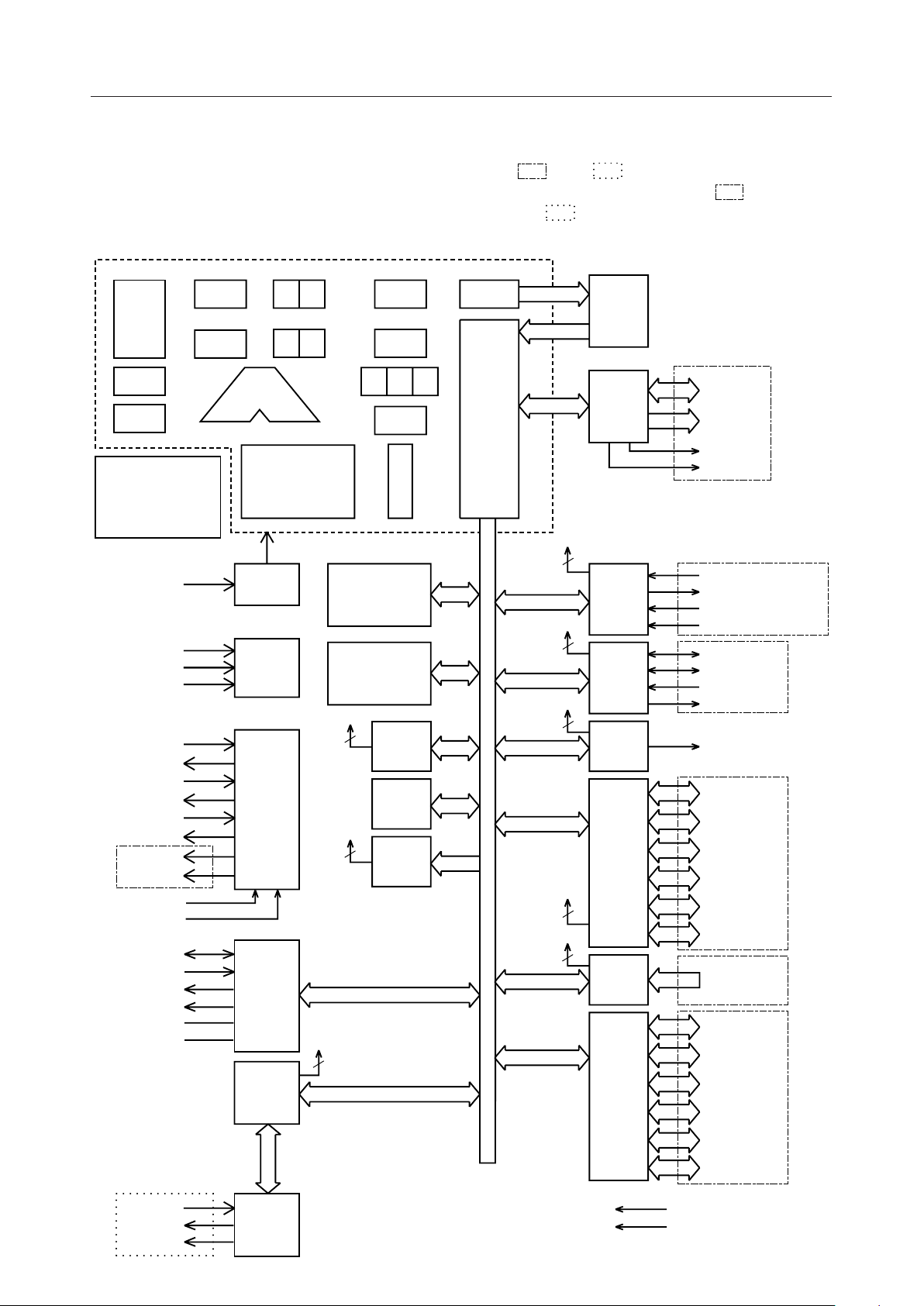
BLOCK DIAGRAM
An asterisk (*) indicates the port secondary function. and indicate that the power is
supplied from V
V
to the circuits corresponding to signal names inside . (V
DDR
for interface)
TIMING
CONTROL
CBR
EBR
to the circuits corresponding to the signal names inside , and from
DDI
H
nX-4/250
L
YX
RA
and V
DDI
PC
A
ROM
16KW
: power supply
DDR
SP
RSP
STACK
CAL.S: 16-level
REG.S: 16-level
RESET
TST1
TST2
TST3
XTM0
XTM1
XT0
XT1
OSC0
OSC1
TBCCLK*
HSCLK*
XTSEL0
XTSEL1
V
DDH
V
DD
V
DDL
V
DD2
CB1
CB2
ALU
INSTRUCTION
DECODER
RST
TST
OSC
BACKUP
Internal
PORT
P0.0-P0.3
P8.2, P8.3
PE.0-PE.3
PF.0-PF.3
INT
C G
RAM
1024N
INT
INT
4
INT
1
3
MIE
IR
TBC
BLD
WDT
Z
BUS
CONTROL
DATA BUS
4
2
1
3
1
INT
INT
INT
INT
INT
EXTMEM
TIMER
8bit ¥ 4
SIO
MELODY
I/O
PORT
INPUT
PORT
OUTPUT
PORT
D0-7*
A0-15*
RD*
WR*
TM0CAP/TM1CAP*
TM0OVF/TM1OVF*
T02CK*
T13CK*
RXC*
TXC*
RXD*
TXD*
MD
P8.0, P8.1
P9.0-P9.3
PA.0-PA.3
PB.0-PB.3
PC.0-PC.3
PD.0-PD.3
P1.0-P1.3
P7.0-P7.3
P6.0-P6.3
P5.0-P5.3
P4.0-P4.3
P3.0-P3.3
P2.0-P2.3
SIGIN
BS1
BS2
POCSAG
Dec
V
DDI
V
DDR
4/32
Page 5
¡ Semiconductor MSM63238
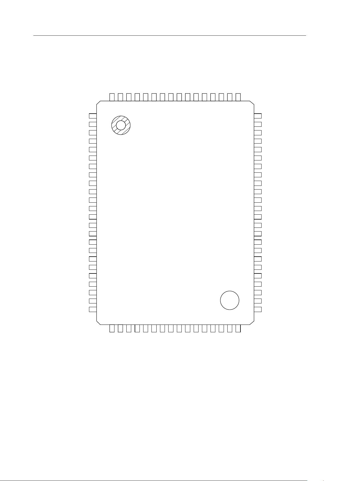
PIN CONFIGURATION (TOP VIEW)
P9.0
P9.1
P9.2
P9.3
PA.0
PA.1
PA.2
PA.3
P4.0
P4.1
P4.2
P4.3
P5.0
P5.2
79
P5.1
78
77
76
75
74
73
72
71
70
69
68
67
66
65
P5.3
80
(NC)
P6.0
P6.1
P6.2
P6.3
P7.0
P7.1
P7.2
P7.3
BS1
BS2
SIGIN
V
DDR
XT0
XT1
TST1
TST2
TST3
OSC0
OSC1
XTSEL0
XTSEL1
XTM0
XTM1
10
11
12
13
14
15
16
17
18
19
20
21
22
23
24
1
2
3
4
5
6
7
8
9
64
63
62
61
60
59
58
57
56
55
54
53
52
51
50
49
48
47
46
45
44
43
42
41
P8.1
(NC)
P8.0
P3.3
P3.2
P3.1
P3.0
P2.3
P2.2
P2.1
P2.0
P1.3
P1.2
P1.1
P1.0
PB.3
PB.2
PB.1
PB.0
PC.3
PC.2
PC.1
PC.0
(NC)
39
38
37
36
35
34
33
32
31
30
29
28
27
26
25
SS
(NC)
DD2
V
DDL
V
DDH
V
CB1
CB2
V
DD
MD
V
RESET
(NC)
DDI
V
PD.0
PD.1
PD.2
80-Pin Plastic QFP
Note: Pins marked as (NC) are no-connection pins which are left open.
40
PD.3
5/32
Page 6
¡ Semiconductor MSM63238
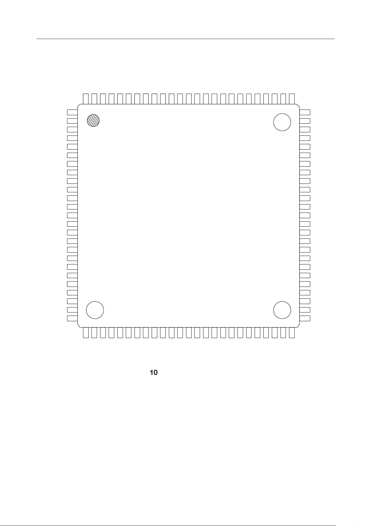
PIN CONFIGURATION (TOP VIEW) (continued)
(NC)
P6.0
(NC)
P5.3
(NC)
P5.2
P5.1
P5.0
P4.3
P4.2
P4.1
999897969594939291
100
90
89 P4.0
88 (NC)
87 PA.3
86 PA.2
85 PA.1
84 PA.0
83 (NC)
82 P9.3
81 P9.2
80 P9.1
79 P9.0
78 (NC)
77 P8.1
76 (NC)
1
P6.1
2
P6.2
3
P6.3
4
P7.0
5
P7.1
6
(NC)
7
P7.2
8
P7.3
9
(NC)
10
BS1
11
BS2
12SIGIN
13(NC)
14V
DDR
15XT0
16XT1
17(NC)
18TST1
19TST2
20TST3
21OSC0 55 (NC)
22OSC1
23XTSEL0
24XTSEL1
25(NC)
75
P8.0
74
P3.3
73
P3.2
72
P3.1
71
(NC)
70
P3.0
69
P2.3
68
P2.2
67
P2.1
66
(NC)
65
P2.0
64 P1.3
63 (NC)
62 P1.2
61 P1.1
60 (NC)
59 P1.0
58 PB.3
57 PB.2
56 PB.1
54 PB.0
53 PC.3
52 PC.2
51 PC.1
2627282930313233343536
DD2VDDL
DDH
(NC)
XTM0
XTM1
(NC)
(NC)
V
CB1
V
CB2
DD
V
37VSS38MD
39RESET
40(NC)
41(NC)
42V
DDI
43PD.0
44PD.1
45PD.2
46PD.3
100-Pin Plastic TQFP
Note: Pins marked as (NC) are no-connection pins which are left open.
47(NC)
48PC.0
49(NC)
50(NC)
6/32
Page 7
¡ Semiconductor MSM63238
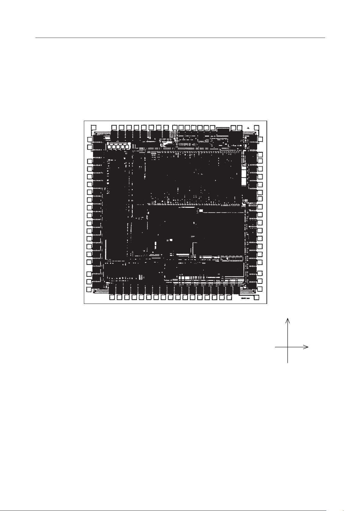
PAD CONFIGURATION
Pad Layout
PC.2 39
PC.3 40
PB.0 41
PB.1 42
PB.2 43
PB.3 44
P1.0 45
P1.1 46
P1.2 47
P1.3 48
P2.0 49
P2.1 50
P2.2 51
P2.3 52
P3.0 53
P3.1 54
P3.2 55
P3.3 56
P8.0 57
PC.138
PC.037
PD.336
PD.235
PD.134
PD.033
DDI
V
32
RESET31
MD30
SS
V
29
DD
V
28
CB227
CB126
DDH
V
25
DDL
V
24
DD2
V
23
XTM122
XTM021
XTSEL120
11
XTSEL019
OSC118
OSC017
TST316
TST215
TST114
XT113
XT012
V
SIGIN10
BS29
BS18
P7.37
P7.26
P7.15
P7.04
P6.33
P6.22
P6.11
DDR
P8.1 58
P9.0 59
P9.1 60
P9.2 61
P9.3 62
PA.0 63
PA.1 64
PA.2 65
PA.3 66
P4.0 67
P4.1 68
P4.2 69
P4.3 70
P5.0 71
P5.1 72
P5.2 73
P5.3 74
Chip Size : 4.55 mm ¥ 4.55 mm
Chip Thickness : 350 mm (typ.)
Coordinate Origin : Chip center
Pad Hole Size : 110 mm ¥ 110 mm
Pad Size : 120 mm ¥ 120 mm
Minimum Pad Pitch : 150 mm
Note: The chip substrate voltage is VSS.
Y
P6.0 75
X
7/32
Page 8
¡ Semiconductor MSM63238
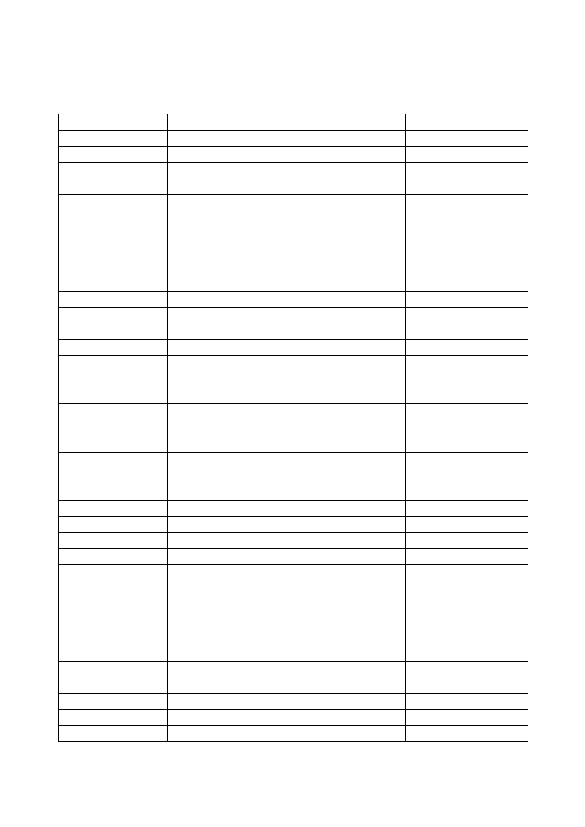
Pad Coordinates
Pad No. Y (µm)X (µm)Pad Name
1 –1897.72123.6P6.1
2 –1701.4P6.2
3 –1505.4P6.3
4 –1231.1P7.0
5 –1034.8P7.1
6 –838.8P7.2
7 –642.5P7.3
8 –446.2BS1
9 –250.2BS2
10 –54.0SIGIN
11 142.0V
DDR
12 338.3XT0
13 495.0XT1
14 691.3TST1
15 887.2TST2
16 1083.6TST3
17 1279.8OSC0
18 1436.5OSC1
19 1819.3XTSEL0
20 2031.2XTSEL1
21 1609.4XTM0
22 1452.8XTM1
23 938.6V
24 782.0V
25 625.3V
DD2
DDL
DDH
26 468.6CB1
27 312.0CB2
28 155.4V
29 –1.3V
DD
SS
30 –219.4MD
31 –405.6RESET
32 –592.2V
DDI
33 –778.4PD.0
34 –964.9PD.1
35 –1151.2PD.2
36 –1337.7PD.3
37 –1523.9PC.0
38 –2031.2PC.1
2123.6
2123.6
2123.6
2123.6
2123.6
2123.6
2123.6
2123.6
2123.6
2123.6
2123.6
2123.6
2123.6
2123.6
2123.6
2123.6
2123.6
2123.6
2107.3
2107.3
2107.3
2107.3
2107.3
2107.3
2107.3
2107.3
2107.3
2107.3
2107.3
2107.3
2107.3
2107.3
2107.3
2107.3
2107.3
2107.3
2107.3
Pad No.
39 1810.6–2123.6PC.2
40 1618.5PC.3
41 1264.2PB.0
42 1072.2PB.1
43 880.1PB.2
44 688.0PB.3
45 496.0P1.0
46 303.9P1.1
47 111.8P1.2
48 –80.6P1.3
49 –272.7P2.0
50 –464.8P2.1
51 –656.8P2.2
52 –848.9P2.3
53 –1041.0P3.0
54 –1233.1P3.1
55 –1529.1P3.2
56 –1721.2P3.3
57 –1913.3P8.0
58 –1552.5P8.1
59 –1370.2P9.0
60 –1187.6P9.1
61 –1005.2P9.2
62 –822.9P9.3
63 –640.6PA.0
64 –458.2PA.1
65 –275.9PA.2
66 –93.6PA.3
67 88.7P4.0
68 271.0P4.1
69 453.4P4.2
70 635.7P4.3
71 818.0P5.0
72 1000.3P5.1
73 1182.7P5.2
74 1365.0P5.3
75 2042.0P6.0
Y (µm)X (µm)Pad Name
–2123.6
–2123.6
–2123.6
–2123.6
–2123.6
–2123.6
–2123.6
–2123.6
–2123.6
–2123.6
–2123.6
–2123.6
–2123.6
–2123.6
–2123.6
–2123.6
–2123.6
–2123.6
–2107.3
–2107.3
–2107.3
–2107.3
–2107.3
–2107.3
–2107.3
–2107.3
–2107.3
–2107.3
–2107.3
–2107.3
–2107.3
–2107.3
–2107.3
–2107.3
–2107.3
–2107.3
8/32
Page 9
¡ Semiconductor MSM63238
PIN DESCRIPTIONS
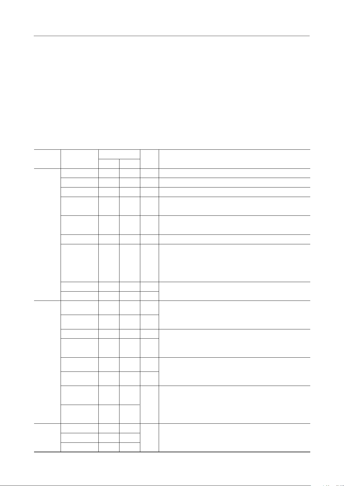
The basic functions of each pin of the MSM63238 are described in Table 1.
A symbol with a slash (/) denotes a pin that has a secondary function.
Refer to Table 2 for secondary functions.
For type, "—" denotes a power supply pin, "I" an input pin, "O" an output pin, and "I/O" an inputoutput pin.
For pin, "GS-BK" denotes an 80-pin flat package (80QFP) and "TS-K" a 100-pin flat package
(100TQFP).
Table 1 Pin Descriptions (Basic Functions)
Function Symbol Type Description
Pin
31
32
13
TS-K
36
37
14
—
—
—
Positive power supply
Negative power supply
Interface power supply for SIGIN, BS1, BS2
V
V
V
GS-BK
DD
SS
DDR
Positive power supply pin for external interface
V
DDI
36
42
—
(power supply for input, output, and I/O ports)
Positive power supply pin for internal logic (internally generated).
Power
Supply
V
V
DDL
DD2
27
26
32
31
—
—
A capacitor (0.1 mF) should be connected between this pin and V
Positive power supply pin for low-speed clock (internally generated)
Voltage multiplier pin for power supply backup
(internally generated).
V
DDH
CB1 Pins to connect a capacitor for voltage multiplier.
CB2
XT0 I
28
29
30
14
33
34
35
15
—
—
—
A capacitor (1.0 mF) should be connected between this pin
SS
.
and V
A capacitor (1.0 mF) should be connected between CB1 and CB2.
Clock oscillation pins for POCSAG decoder.
A 32.768 kHz, 38.4 kHz, or 76.8 kHz crystal and capacitor (C
XT1 O
XTM0 I
15
23
16
27
should be connected to these pins.
Low-speed clock oscillation pins for CPU.
A 32.768 kHz crystal and capacitor (C
Oscillation
XTM1 O
OSC0 I
24
19
28
21
to these pins.
High-speed clock oscillation pins.
A ceramic resonator and capacitors (C
OSC1 O
20
22
oscillation resistor (R
) should be connected to these pins.
OS
Low-speed CPU clock select pins.
Test
XTSEL0
XTSEL1
TST1 Input pins for testing.
TST2 I
TST3
21
22
16
17
18
23
24
18
19
20
These pins are used to select a low-speed CPU clock.
I
Because these are high impedance inputs, be sure to tie these
pins to V
or VSS.
DD
Pull-down resistors are internally connected to these pins.
The user cannot use these pins.
) should be connected
GM
, CL1) or external
L0
SS
.
)
G
9/32
Page 10
¡ Semiconductor MSM63238
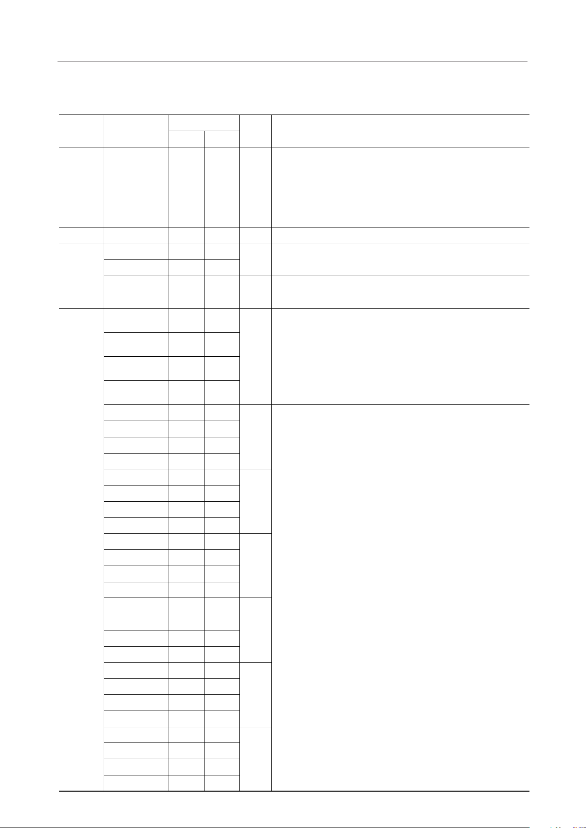
Table 1 Pin Descriptions (Basic Functions) (continued)
33
10
11
12
50
51
52
Pin
TS-KGS-BK
Reset input pin.
Setting this pin to "H" level puts this device into a reset state.
hen, setting this pin to "L" level starts executing an instruction
39
38
10
11
12
59
61
62
64
T
from address 0000H.
A pull-down resistor is internally connected to this pin.
Battery saving outputs.
O
Signals to control intermittent operations of RF receiver.
Receive data input pin.
Input pin for receive data from RF receiver.
4-bit input port.
Pull-up resistor input, pull-down resistor input, or
high-impedance input is selectable for each bit.
I
Function Symbol Type Description
Reset 34
Melody
POCSAG
Decoder
RESET I
MD O Melody output pin (normal phase)
BS1
BS2
SIGIN I
P1.0/INT5
P1.1/INT5
P1.2/INT5
P1.3/INT5 53
Port
P2.0
P2.1
P2.2
P2.3
P3.0
P3.1
P3.2
P3.3
P4.0/A0
P4.1/A1
P4.2/A2
P4.3/A3
P5.0/A4
P5.1/A5
P5.2/A6
P5.3/A7
P6.0/A8
P6.1/A9
P6.2/A10
P6.3/A11
P7.0/A12
P7.1/A13
P7.2/A14
P7.3/A15 9
54
55
56
57
58
59
60
61
73
74
75
76
77
78
79
80
65
67
68
69
70
72
73
74
89
90
91
92
93
94
95
97
2
3
4
5
6
7
8
99
1
2
3
4
5
7
8
4-bit output ports.
P-channel open drain output, N-channel open drain output,
O
CMOS output, or high-impedance output is selectable for each
bit.
O
O
O
O
O
10/32
Page 11

¡ Semiconductor MSM63238
Table 1 Pin Descriptions (Basic Functions) (continued)
Function Symbol Type Description
P8.0/RD
P8.1/WR
P9.0/D0
P9.1/D1
P9.2/D2
P9.3/D3
PA.0/D4
PA.1/D5
PA.2/D6
PA.3/D7
PB.0/INT0/
TM0CAP/
TM0OVF
PB.1/INT0/
TM1CAP/
TM1OVF
Port
PB.2/INT0/
T02CK
PB.3/INT0/
T13CK
PC.0/INT1/
RXD
PC.1/INT1/
TXC
PC.2/INT1/
RXC
PC.3/INT1/
TXD
PD.0 37
PD.1 38
PD.2 39
PD.3 40
Pin
GS-BK TS-K
62
64
65
66
67
68
69
70
71
72
46
47
48
49
42
43
44
45
75
77
79
80
81
82
84
85
86
87
54
56
57
58
48
51
52
53
43
44
45
46
I/O
I/O
I/O
I/O
I/O
I/O
2-bit input-output port and 4-bit input-output ports.
In input mode, pull-up resistor input, pull-down resistor input,
or high-impedance input is selectable for each bit.
In output mode, P-channel open drain output, N-channel open
drain output, CMOS output, or high-impedance output is
selectable for each bit.
11/32
Page 12

¡ Semiconductor MSM63238
Table 2 shows the secondary functions of each pin of the MSM63238.
Table 2 Pin Descriptions (Secondary Functions)
Function Symbol Type Description
PB.0/INT0
PB.1/INT0 47
PB.2/INT0 48
PB.3/INT0 49
PC.0/INT1 42 External 1 interrupt input pins.
External
Interrupt
Capture
PC.1/INT1 43
PC.2/INT1 44
PC.3/INT1 45
P1.0/INT5
P1.1/INT5 51
P1.2/INT5 52
P1.3/INT5 53
PB.0/TM0CAP 46
PB.1/TM1CAP 47
Pin
GS-BK TS-K
46
50 External 5 interrupt input pins.
54
56
57
58
48
51
52
53
59
61
62
64
54
56
External 0 interrupt input pins.
The change of input signal level causes an interrupt to occur.
I
The Port B Interrupt Enable register (PBIE) enables or
disables an interrupt for each bit.
The change of input signal level causes an interrupt to occur.
I
The Port C Interrupt Enable register (PCIE) enables or
disables an interrupt for each bit.
The change of input signal level causes an interrupt to occur.
I
The Port 1 Interrupt Enable register (P1IE) enables or
disables an interrupt for each bit.
I
Timer 0 capture trigger input pin.
I
Timer 1 capture trigger input pin.
12/32
Page 13

¡ Semiconductor MSM63238
Table 2 Pin Descriptions (Secondary Functions) (continued)
Function Symbol Type Description
PB.0/TM0OVF 46
Timer
Oscillation
Output
Serial
Port
PB.1/TM1OVF 47
PB.2/T02CK 48
PB.3/T13CK 49
PD.2/TBCCLK 39
PD.3/HSCLK 40
PC.0/RXD 42
PC.1/TXC 43
PC.2/RXC 44
Pin
GS-BK TS-K
54
56
57
58
45
46
48
51
52
O
O
O
O
I/O
I/O
Timer 0 overflow flag output pin.
Timer 1 overflow flag output pin.
I
External clock input pin for timer 0 and timer 2.
I
External clock input pin for timer 1 and timer 3.
Low-speed oscillation clock output pin
High-speed oscillation clock output pin
I
Serial port receive data input pin
Sync serial port clock input-output pin.
Transmit clock output when this device is used as a master
processor.
Transmit clock input when this device is used as a slave
processor.
Sync serial port clock input-output pin.
Receive clock output when this device is used as a master
processor.
Receive clock input when this device is used as a slave
processor.
PC.3/TXD 45
53
O
Serial port transmit data output pin.
13/32
Page 14

¡ Semiconductor MSM63238
Table 2 Pin Descriptions (Secondary Functions) (continued)
Function Symbol Type Description
P4.0/A0
P4.1/A1
P4.2/A2
P4.3/A3
P5.0/A4
P5.1/A5
P5.2/A6
P5.3/A7
P6.0/A8
P6.1/A9
P6.2/A10
P6.3/A11
External
Memory
P7.0/A12
P7.1/A13
P7.2/A14
P7.3/A15 9
P9.0/D0
P9.1/D1
P9.2/D2
P9.3/D3
PA.0/D4
PA.1/D5
PA.2/D6
PA.3/D7 72
P8.0/RD 62
P8.1/WR 64
Pin
GS-BK TS-K
73 Address output bus for external memory
74
75
76
77
78
79
80
2
3
4
5
6
7
8
65
66
67
68
69
70
71
89
90
91
92
93
94
95
97
99
79
80
81
82
84
85
86
87
75
77
O
1
2
3
4
5
7
8
Data bus for external memory
I/O
O
Read signal output pin for external memory (negative logic)
O
Write signal output pin for external memory (negative logic)
14/32
Page 15
¡ Semiconductor MSM63238
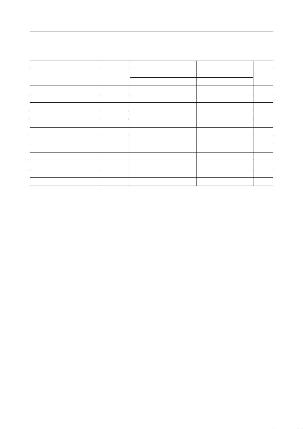
ABSOLUTE MAXIMUM RATINGS
(VSS = 0 V)
Parameter Symbol Condition Rating Unit
Power Supply Voltage 1 V
Power Supply Voltage 2 V
Power Supply Voltage 3 V
Power Supply Voltage 4 V
Power Supply Voltage 5 V
Input Voltage 1 V
Input Voltage 2 V
Input Voltage 3
Output Voltage 1
Output Voltage 2
Output Voltage 3
Output Voltage 4
V
V
V
V
Storage Temperature
DDI
DDR
DDH
DDL
V
OUT1
OUT2
OUT3
OUT4
T
STG
DD
IN1
IN2
IN3
Backup used, Ta = 25°C –0.3 to +3.0
Backup not used, Ta = 25°C
–0.3 to +6.0
Ta = 25°C –0.3 to +6.0 V
Ta = 25°C –0.3 to +6.0 V
Ta = 25°C –0.3 to +6.0 V
Ta = 25°C –0.3 to +6.0 V
VDD Input, Ta = 25°C –0.3 to VDD + 0.3 V
V
Input, Ta = 25°C –0.3 to V
DDI
V
Input, Ta = 25°C –0.3 to V
DDR
+ 0.3 V
DDI
+ 0.3 V
DDR
VDD output, Ta = 25°C –0.3 to VDD + 0.3 V
V
output, Ta = 25°C –0.3 to V
DDI
V
output, Ta = 25°C –0.3 to V
DDR
V
output, Ta = 25°C –0.3 to V
DDH
—
–55 to +150 °C
+ 0.3 V
DDI
+ 0.3 V
DDR
+ 0.3 V
DDH
V
15/32
Page 16

¡ Semiconductor MSM63238
RECOMMENDED OPERATING CONDITIONS
• When backup is used
(V
= 0 V)
SS
Parameter Symbol Condition Range Unit
Operating Temperature T
Operating Voltage
V
V
Crystal Oscillation Frequency
f
Ceramic Oscillation Frequency
External RC Oscillator Resistance
V
DDR
f
XTM
f
CM
R
op
DD
DDI
XT
OS
—
— 0.9 to 2.7 V
—
—
—
—
VDD = 1.2 to 2.7 V
VDD = 1.2 to 2.7 V
–20 to +70 °C
0.9 to 5.5 V
0.9 to 5.5 V
30 to 80 kHz
30 to 35 kHz
300k to 500k
200k to 1MVDD = 1.5 to 2.7 V
100 to 300
50 to 300VDD = 1.5 to 2.7 V
Hz
k
W
• When backup is not used
Parameter Symbol Condition Range Unit
Operating Temperature T
Operating Voltage
Crystal Oscillation Frequency
Ceramic Oscillation Frequency
External RC Oscillator Resistance
V
V
V
f
R
op
DD
DDI
DDR
f
XT
XTM
f
CM
OS
—
— 1.8 to 5.5 V
—
—
—
—
VDD = 2.2 to 5.5 V
VDD = 2.2 to 5.5 V
(V
SS
–20 to +70 °C
1.8 to 5.5 V
1.8 to 5.5 V
30 to 80 kHz
30 to 35 kHz
300k to 500kVDD = 1.8 to 5.5 V
300k to 1M
200k to 2MVDD = 2.7 to 5.5 V
100 to 300VDD = 1.8 to 5.5 V
50 to 300
30 to 300VDD = 2.7 to 5.5 V
= 0 V)
Hz
kW
16/32
Page 17

¡ Semiconductor MSM63238
ELECTRICAL CHARACTERISTICS
DC Characteristics
(VDD = V
Parameter Symbol Condition
V
Voltage (Backup used) V
DDH
Voltage V
V
DDL
V
Voltage V
DD2
Crystal Oscillation Start
Voltage
Crystal Oscillation Hold Voltage V
Crystal Oscillation Stop Detect
Time
External Crystal Oscillator
Capacitance
C
Internal Crystal Oscillator
Capacitance
C
Internal RC Oscillator
Capacitance
POR Voltage
Non-POR Voltage
DDI
T
G
D
V
V
= V
DDH
DDL
DD2
V
STA
HOLD
STOP
, C
, C
C
OS
POR1
POR2
= 0.9 to 5.5 V, VSS = 0 V, Ta = –20 to +70°C unless otherwise specified)
DDR
Max.Typ.Min.
Unit
High speed clock stop
V
= 1.5 V
DD
, C12 = 1 mF
C
h
2.8 — 3.0 V
High speed clock oscillation
(Ceramic oscillation, 1 MHz)
V
= 1.5 V
DD
C
, C12 = 1 mF
h
2.0 — 2.7 V
High speed clock stop 1.0 1.5 2.0 V
High speed clock oscillation
(V
= 1.2 to 5.5 V)
DD
1.2 5.5 V
—
— 1.0 2.0 V1.5
Oscillation start time: within
5 seconds
1.2 V
—
—
0.9 V——Backup used (Ta = 25°C)
1.0 V——Backup used
Backup not used
—
GM
DM
—
—
—
VDD = 1.5 V 0.0 0.4 V
= 3.0 V
DD
VDD = 1.5 V 1.2 1.5 V
V
= 3.0 V
DD
1.7 V
0.1 5.0 ms
525pF
—
—
—
—
20 25 30 pF
81216pF
—
0.0 0.7 VV
—
—
2.0 3.0 V
—
Mea-
suring
Circuit
1
Notes: 1. "T
reset occurs.
2. "POR" denotes Power On Reset.
3. "V
up to VDD.
4. "V
again rises up to VDD.
" indicates that if the crystal oscillator stops over the value of T
STOP
" indicates that POR occurs when VDD falls from VDD to V
POR1
" indicates that POR does not occur when VDD falls from VDD to V
POR2
, the system
STOP
and again rises
POR1
POR2
and
17/32
Page 18

¡ Semiconductor MSM63238
DC Characteristics (continued)
• When backup is used
(VDD = V
DDI
Parameter Symbol Condition
CPU in HALT mode.
(High-speed clock oscillation stop)
Supply Current 1
I
DD1
Decoder in HALT mode.
(Decoder oscillation stop)
CPU in HALT mode.
(High-speed clock oscillation stop)
Supply Current 2
I
DD2
Decoder in carrier on state.
(76.8 kHz operation)
CPU in HALT mode.
(High-speed clock oscillation stop)
Supply Current 3
I
DD3
Decoder in data receiving state.
(76.8 kHz operation)
CPU in operation at 32 kHz.
(High-speed clock oscillation stop)
Supply Current 4
I
DD4
Decoder in HALT mode.
(Decoder oscillation stop)
CPU in operation at high speed.
Supply Current 5
I
DD5
(RC oscillation, R
Decoder in HALT mode.
(Decoder oscillation stop)
CPU in operation at high speed.
Supply Current 6
I
DD6
(Ceramic oscillation, 1 MHz)
Decoder in HALT mode.
(Decoder oscillaiton stop)
= 1.5 V, VSS = 0 V, Ta = –20 to +70°C unless otherwise specified)
Mea-
suring
Max.Typ.Min.
Unit
Circuit
356.0—
mA
mA
8035—
20085—
mA
1
4022—
mA
= 51 kW)
OS
800600—
900700—
mA
mA
18/32
Page 19
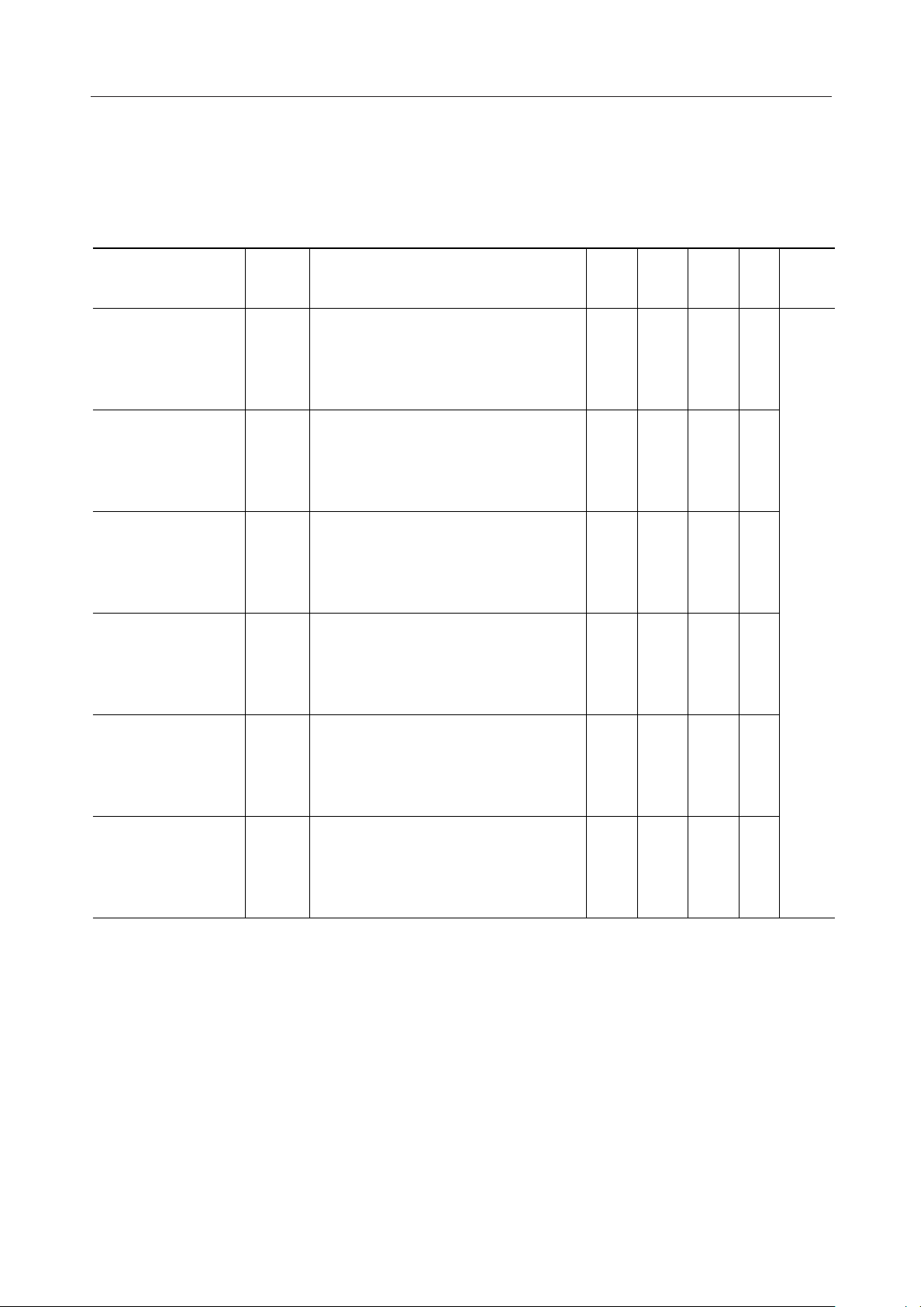
¡ Semiconductor MSM63238
DC Characteristics (continued)
• When backup is not used
(VDD = V
DDI
Parameter Symbol Condition
CPU in HALT mode.
(High-speed clock oscillation stop)
Supply Current 1
I
DD1
Decoder in HALT mode.
(Decoder oscillation stop)
CPU in HALT mode.
(High-speed clock oscillation stop)
Supply Current 2
I
DD2
Decoder in carrier on state.
(76.8 kHz operation)
CPU in HALT mode.
(High-speed clock oscillation stop)
Supply Current 3
I
DD3
Decoder in data receiving state.
(76.8 kHz operation)
CPU in operation at 32 kHz.
(High-speed clock oscillation stop)
Supply Current 4
I
DD4
Decoder in HALT mode.
(Decoder oscillation stop)
CPU in operation at high speed.
(RC oscillation, R
Supply Current 5
I
DD5
Decoder in HALT mode.
(Decoder oscillation stop)
CPU in operation at high speed.
(Ceramic oscillation, 2 MHz)
Supply Current 6
I
DD6
Decoder in HALT mode.
(Decoder oscillation stop)
= 3.0 V, VSS = 0 V, Ta = –20 to +70°C unless otherwise specified)
Mea-
suring
Max.Typ.Min.
Unit
Circuit
203.0—
mA
4017—
mA
10042—
mA
1
2510—
mA
= 51 kW)
OS
600450—
1000800—
mA
mA
19/32
Page 20

¡ Semiconductor MSM63238
DC Characteristics (continued)
(VDD = V
DDI
= V
DDH
= V
DDR
Parameter Symbol Condition
Output Current 1
(P2.0 to P2.3)
(P3.0 to P3.3)
(P4.0 to P4.3)
.
.
.
(PC.0 to PC.3)
I
OH1
I
OL1
V
= V
– 0.5 V –1.0 mA
DDI
= 0.5 V 6.0 mA
V
OH1
OL1
(PD.0 to PD.3)
Output Current 2
(MD)
I
OH2
I
OL2
V
= VDD – 0.7 V –2.0 mA
OH2
V
= 0.7 V 11.0 mA
OL2
Output Current 3
(BS1, BS2)
Output Current 4
(OSC1)
I
OH3
I
OL3
I
OH4R
I
OL4R
I
OH4C
I
OL4C
V
= V
OH3
V
= 0.5 V 16.0 mA
OL3
V
OH4R
– 0.5 V –2.0 mA
DDR
= V
– 0.5 V
DDH
(RC oscillation)
V
= 0.5 V
OL4R
(RC oscillation)
V
= V
OH4C
DDH
– 0.5 V
(ceramic oscillation)
V
= 0.5 V
OL4C
(ceramic oscillation)
Output Leakage
(P2.0 to P2.3)
I
OOH
VOH = V
DDI
(P3.0 to P3.3)
(P4.0 to P4.3)
.
.
.
I
OOL
VOL = V
SS
(PD.0 to PD.3)
= 3.0 V, VSS = 0 V, Ta = –20 to +70°C unless otherwise specified)
Mea-
Unit
Min.
Typ.
Max.
suring
Circuit
V
V
V
V
V
V
V
V
V
V
V
V
V
V
V
V
V
V
V
V
V
V
V
DDI
DDI
DDI
DDI
DDI
DDI
DD
DD
DD
DD
DD
DD
DDR
DDR
DDR
DDR
DDR
DDR
DD
DD
DD
DD
DD
= 1.5 V
= 3.0 V
= 5.0 V
= 1.5 V
= 3.0 V
= 5.0 V
= 1.5 V
= 3.0 V
= V
DDH
= 1.5 V
= 3.0 V
= V
DDH
= 1.5 V
= 3.0 V
= 5.0 V
= 1.5 V
= 3.0 V
= 5.0 V
= V
DDH
= V
DDH
DDH
= V
DDH
DDH
= V
DDH
DDH
= V
DDH
–2.5
–6.0
–8.5
–4.0
–11.0
= 5.0 V
–14.0
= 5.0 V
–7.0
–16.0
–24.0
= 3.0 V
–2.5
= 5.0 V –0.5 mA–1.7–3.5
= 3.0 V
= 5.0 V 3.5 mA1.80.5
= 3.0 V
= 5.0 V –100 mA–240–400
= 3.0 V
= 5.0 V 400 mA210100
–1.0
0.4
1.0
1.5
0.5
2.0
4.0
1.0
2.0
3.0
—
–1.4
–3.5
–5.0
1.4
3.0
3.7
–2.0
–6.0
–9.0
2.0
5.5
7.0
–4.5
–10.0
–14.0
4.0
8.0
9.5
–1.3
—
—
–0.4 mA
–1.5 mA
2.5 mA
8.5 mA
–0.5 mA
–4.0 mA
4.0 mA
14.0 mA
–1.0 mA
–3.0 mA
7.0 mA
24.0 mA
–0.25 mA
2.5 mA1.50.25VDD = V
–60 mA–160–300VDD = V
300 mA17060VDD = V
1.0 mA
— mA
2
20/32
Page 21

¡ Semiconductor MSM63238
DC Characteristics (continued)
(VDD = V
DDI
= V
DDH
= V
DDR
Parameter Symbol Condition
Input Current 1
V
= V
IH1
(P1.0 to P1.3)
(P8.0, P8.1)
(P9.0 to P9.3)
.
.
.
(PD.0 to PD.3)
Input Current 2
(SIGIN)
Input Current 3
(OSC0)
I
I
I
IH1Z
I
IL1Z
I
IH2Z
I
IL2Z
I
I
IH3R
I
IL3R
I
IH3C
I
IL3C
IH1
IL1
IL3
(when pulled down)
V
(when pulled up)
V
V
V
V
V
(when pulled up)
V
V
V
(ceramic oscillation)
V
(ceramic oscillation)
DDI
= V
IL1
SS
= V
IH1
= V
IL1
= V
IH2
= V
IL2
= V
IL3
= V
IH3
= VSS (RC oscillation) 0.0 mA—–1.0
IL3
= V
IH3
= V
IL3
(in a high impedance state) 1.0 mA—0.0
DDI
(in a high impedance state) 0.0 mA—–1.0
SS
DDR
SS
SS
(RC oscillation) 1.0 mA—0.0
DDH
DDH
SS
Input Current 4
(RESET)
I
I
IH4
IL4
V
= V
IH4
DD
V
= V
IL4
SS
Input Current 5
(TST1, TST2, TST3)
(XTSEL0, XTSEL1)
I
I
I
IH6Z
I
IL6Z
IH5
IL5
V
= V
IH5
DD
V
= V
IL5
SS
V
= V
IH6
DD
V
= V
IL6
SS
= 3.0 V, VSS = 0 V, Ta = –20 to +70°C unless otherwise specified)
Mea-
Unit
Min.
Typ.
Max.
suring
Circuit
V
DDI
V
DDI
V
DDI
V
DDI
V
DDI
V
DDI
= 1.5 V
= 3.0 V
= 5.0 V
= 1.5 V
= 3.0 V
= 5.0 V
2
30
70
–45
–260
–650
20
120
350
–20
–120
–350
45 mA
260 mA
650 mA
–2 mA
–30 mA
–70 mA
1.0 mA—0.0
0.0 mA—–1.0
= V
V
DD
V
= V
DD
DDH
DDH
= 3.0 V
= 5.0 V
–350
–750
–170
–450
–30 mA
–200 mA
3
V
= V
DD
V
= V
DD
V
= V
DD
V
= V
DD
= 1.5 V
V
DD
V
= 3.0 V 2400 mA1100150
DD
= V
V
DD
= 3.0 V
DDH
= 5.0 V
DDH
= 3.0 V
DDH
= 5.0 V
DDH
= 5.0 V 5.0 mA2.70.5
DDH
0.1
0.75
–1.0
–3.0
10
0.5
1.5
–0.5
–1.5
180
1.0 mA
3.0 mA
–0.1 mA
–0.75 mA
350 mA
0.0 mA—–1.0
1500 mA75050VDD = 1.5 V
V
= 3.0 V 5.5 mA3.00.5
DD
= V
V
DD
= 5.0 V 11.0 mA6.50.25
DDH
0.0 mA—–1.0
1.0 mA—0.0Input Current 6
0.0 mA—–1.0
21/32
Page 22

¡ Semiconductor MSM63238
DC Characteristics (continued)
(VDD = V
Parameter Symbol Condition
Input Voltage 1
(P1.0 to P1.3)
(P8.0, P8.1)
(P9.0 to P9.3)
.
.
.
(PD.0 to PD.3)
Input Voltage 2
(SIGIN)
Input Voltage 3
(OSC0)
Input Voltage 4
(RESET, TST1, TST2, TST3,
XTSEL0, XTSEL1)
Hysteresis Width 1
(P1.0 to P1.3)
(P8.0, P8.1)
.
.
.
(PD.0 to PD.3)
DDI
= V
V
V
V
V
V
V
V
V
DV
IH1
IL1
IH2
IL2
IH3
IL3
IH4
IL4
T1
DDH
= V
= 3.0 V, VSS = 0 V, Ta = –20 to +70°C unless otherwise specified)
DDR
Unit
V
DDI
V
DDI
V
DDI
V
DDI
V
DDI
V
DDI
V
DDR
V
DDR
V
DDR
V
DDR
V
DDR
V
DDR
VDD = V
VDD = V
VDD = V
VDD = V
V
DD
Max.Typ.Min.
= 1.5 V 1.2 — 1.5 V
= 3.0 V 2.4 — 3.0 V
= 5.0 V 4.0 — 5.0 V
= 1.5 V 0.0 — 0.3 V
= 3.0 V 0.0 — 0.6 V
= 5.0 V 0.0 — 1.0 V
= 1.5 V 1.2 — 1.5 V
= 3.0 V 2.4 — 3.0 V
= 5.0 V 4.0 — 5.0 V
= 1.5 V 0.0 — 0.3 V
= 3.0 V 0.0 — 0.6 V
= 5.0 V 0.0 — 1.0 V
= 3.0 V 2.4 — 3.0 V
DDH
= 5.0 V 4.0 — 5.0 V
DDH
= 3.0 V 0.0 — 0.6 V
DDH
= 5.0 V 0.0 — 1.0 V
DDH
= 1.5 V 1.35 — 1.5 V
VDD = 3.0 V 2.4 — 3.0 V
= V
V
DD
= 5.0 V 4.0 — 5.0 V
DDH
VDD = 1.5 V 0.0 — 0.15 V
VDD = 3.0 V 0.0 — 0.6 V
V
DD
= V
V
V
V
= 5.0 V 0.0 — 1.0 V
DDH
= 1.5 V 0.05 0.1 0.3 V
DDI
= 3.0 V 0.2 0.5 1.0 V
DDI
= 5.0 V 0.25 1.0 1.5 V
DDI
Mea-
suring
Circuit
4
Hysteresis Width 2
(RESET, TST1, TST2, TST3,
XTSEL0, XTSEL1)
Input Pin Capacitance
(P1.0 to P1.3)
(P8.0, P8.1)
(P9.0 to P9.3)
.
.
.
(PD.0 to PD.3)
DV
C
VDD = 1.5 V 0.05 0.1 0.3 V
= 3.0 V 0.2 0.5 1.0 V
T2
IN
V
DD
V
DD
= V
= 5.0 V 0.25 1.0 1.5 V
DDH
———5pF
1
22/32
Page 23
¡ Semiconductor MSM63238
p
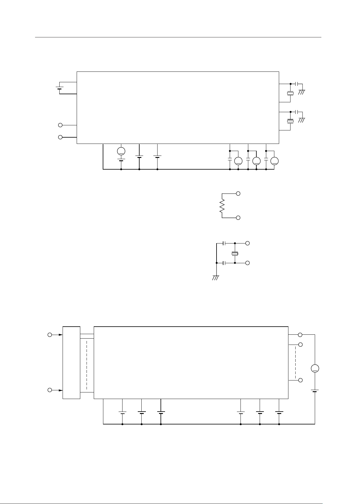
Measuring circuit 1
C
C
b12
CB1
XT0
CB2
XT1
XTM0
G
C
GM
76.8 kHz
Crystal
(*1)
q
w
Cl, C
2
Ch, C
b12
CG, C
C
L0
C
L1
Ceramic Resonator
OSC0
OSC1
GM
XTM1
V
SS
V
DD
A
: 0.1 mF
: 1 mF
V
V
DDI
DDR
V
DDH
C
h
V V
V
V
C
l
DDL
DD2
C
2
V
*1 RC Oscillator
q
32.768 kHz
Crystal
: 15 pF
R
: 30 pF
: 30 pF
: CSB1000J (1 MHz)
CSA2.00MG (2 MHz)
(Murata MFG.-make)
OS
w
Ceramic Oscillator
q
C
L0
Ceramic Resonator
w
C
L1
Measuring circuit 2
V
IH
(*2)
V
IL
*2 Input logic circuit to determine the specified measuring conditions.
*3 Measured at the s
V
V
SS
DD
ecified output pins.
(*3)
OUTPUTINPUT
A
V
V
DDI
DDR
V
DDH
V
DDL
V
DD2
23/32
Page 24

¡ Semiconductor MSM63238
Measuring circuit 3
(*4)
A
INPUT OUTPUT
V
SS
V
DD
V
V
DDI
DDR
V
DDH
V
DDL
V
DD2
Measuring circuit 4
V
IH
(*4)
V
IL
*4 Measured at the specified input pins.
INPUT OUTPUT
V
SS
V
DD
V
V
DDI
DDR
V
DDH
V
DDL
V
DD2
Waveform
Monitoring
24/32
Page 25

¡ Semiconductor MSM63238
AC Characteristics (Serial Interface, Serial Port)
(VDD = V
= 0.9 to 5.5 V, V
DDR
DDH
otherwise specified)
(1) Synchronous Communication
Parameter Symbol Condition Unit
t
f
r
TXC/RXC Input "L" Level
Pulse Width
TXC/RXC Input "H" Level
Pulse Width
TXC/RXC Output Cycle Time
t
CWL
t
CWH
CYC
t
CYC1(O)
CYC2(O)
DDR
DS
DH
= 1.8 to 5.5 V, VSS = 0 V, V
— ms— 1.0
— ms— 1.0
— ms——
— ms——
— ms——
CPU in operation state at 32 kHz ms30.5 —
= 5.0 V, Ta = –20 to +70°C unless
DDI
—TXC/RXC Input Fall Time
—TXC/RXC Input Rise Time t
0.8
0.8
2.0TXC/RXC Input Cycle Time t
—
CPU in operation at 2 MHz
= V
V
DD
= 2.7 V to 5.5 V
DDH
Output load capacitance 10 pF ms— 0.4
— ms——
— ms——
—t
—TXD Output Delay Time t
0.5RXD Input Setup Time t
0.8RXD Input Hold Time t
Max.Typ.Min.
ms0.5 —
Synchronous communication timing
("H" level = 4.0 V, "L" level = 1.0 V)
t
CYC
TXC (PC.1)/
RXC (PC.2)
t
DDR
TXD (PC.3)
t
DS
RXD (PC.0)
5 V (V
DDI
)
0 V (VSS)
t
r
t
CWH
t
DDR
t
f
t
CWL
5 V (V
DDI
)
0 V (VSS)
t
DH
t
DS
5 V (V
DDI
)
0 V (VSS)
25/32
Page 26
¡ Semiconductor MSM63238
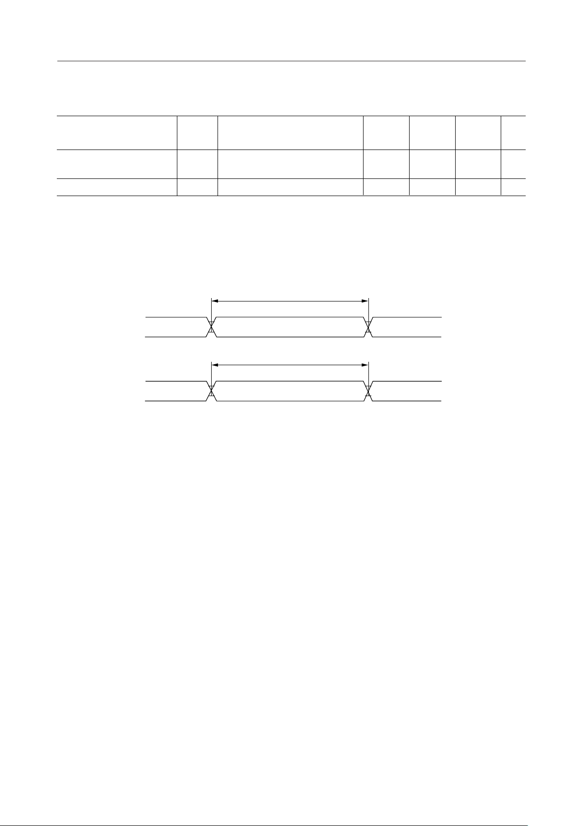
(2) UART Communication
Parameter Symbol Condition Unit
Transmit Baud Rate
T
BRT
BRT
UART communication timing
("H" level = 4.0 V, "L" level = 1.0 V)
TXD (PC.3)
RXD (PC.0)
T
= 1/f
BRT
TCR = 1/f
= 1/f
BRT
T
BRT
R
BRT
BRT
OSC
BRT
Max.Typ.Min.
T
BRT–TCR
R
¥0.97Receive Baud Rate R
BRT
f
: Baud rates (1200, 2400, 4800, 9600 bps)
BRT
BRT
BRT
T
R
5 V (V
BRT+TCR
¥1.03R
BRT
)
DDI
0 V (VSS)
5 V (V
DDI
)
0 V (VSS)
sT
sR
26/32
Page 27

¡ Semiconductor MSM63238
AC Characteristics (External Memory Interface)
(VDD = V
= 0.9 to 5.5 V, V
DDR
= 1.8 to 5.5 V, VSS = 0 V, V
DDH
otherwise specified)
(1) Reading from External Memory
(a) When CPU operates at 32.768 kHz
Parameter
Read Cycle Time
RD Output Delay Time
Output Valid Time
External Memory Output Delay Time
(b) When CPU operates at 2 MHz (V
Parameter
Read Cycle Time
RD Output Delay Time
Output Valid Time
External Memory Output Delay Time
Symbol Condition Min. Typ. Max. Unit
t
RC
t
OE
t
OHA
t
DO
= 2.7 to 5.5 V)
DDH
Symbol Condition Min. Typ. Max. Unit
t
RC
t
OE
t
OHA
t
DO
—
—
—
—
—
—
—
—
= 5.0 V, Ta = –20 to +70°C unless
DDI
—
—
—
—
1.0 ms
—
—
—
61.0 ms
—
—
—
—
—
—
—
—
5.0
5.0
5.0
—
100
100
150
ms
ms
ms
ns
ns
ns
AC characteristics timing
("H" level = 4.0 V, "L" level = 1.0 V)
System clock
P7 - P4
(A15 - A0)
P8.0
(RD)
PA, P9
(D7 - D0)
Port setup value
Port setup value
MOVXB obj, xadr16
MOVXB obj, [RA]
Address output Port setup value
t
OE
S2S1S2S1S2S1
t
RC
5 V (V
0 V (V
5 V (V
0 V (V
t
OHA
5 V (V
Port setup valueInput data
t
DO
0 V (V
DDI
SS
DDI
SS
DDI
SS
)
)
)
)
)
)
27/32
Page 28
¡ Semiconductor MSM63238
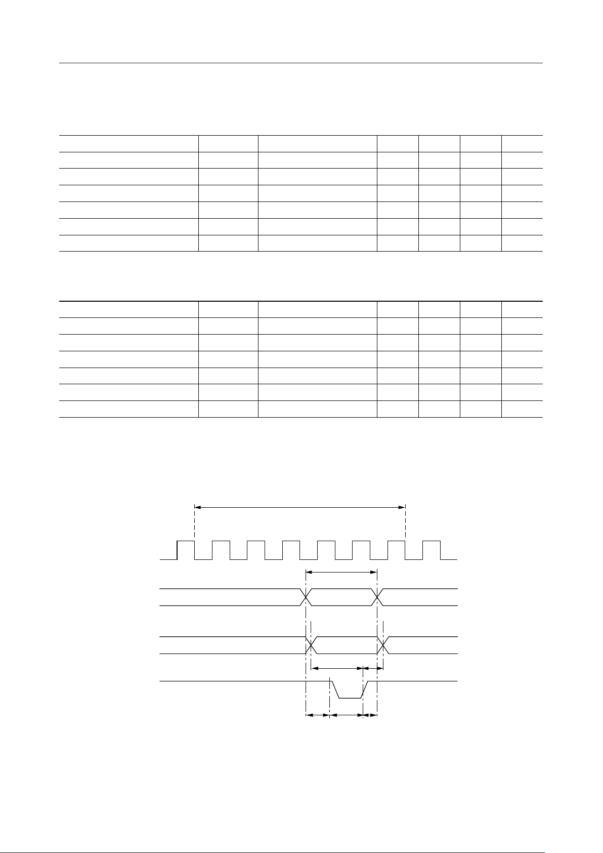
(2) Writing to External Memory
(a) When CPU operates at 32.768 kHz
Parameter
Write Cycle Time
Address Setup Time
Write Time
Write Recovery Time
Data Setup Time
Data Hold Time
Symbol Condition Min. Typ. Max. Unit
t
t
t
t
t
WC
AS
t
W
WR
DS
DH
—
—
—
—
—
—
—
—
—
—
—
—
61.0 ms
30.5
15.3
15.3
45.8
15.3
—
—
—
—
—
—
ms
ms
ms
ms
ms
(b) When CPU operates at 2 MHz (V
Parameter
Write Cycle Time
Address Setup Time
Write Time
Write Recovery Time
Data Setup Time
Data Hold Time
= 2.7 to 5.5 V)
DDH
Symbol Condition Min. Typ. Max. Unit
t
WC
t
AS
t
W
t
WR
t
DS
t
DH
AC characteristics timing
("H" level = 4.0 V, "L" level = 1.0 V)
MOVXB [RA], obj or MOVXB xadr16, obj
System clock
—
—
—
—
—
—
t
WC
1.0 ms
0.4
0.2
0.2
0.7
0.2
—
—
—
—
—
—
—
—
—
—
—
—
ms
ms
ms
ms
ms
S2S1S2S1S2S1
(A15 - A0)
PA, P9
(D7 - D0)
P8.1
(WR)
Address output Port setup valuePort setup valueP7 - P4
5 V (V
0 V (V
5 V (V
Output data Port setup valuePort setup value
t
t
DS
DH
0 V (V
5 V (V
0 V (V
t
tWt
AS
WR
DDI
SS
DDI
SS
DDI
SS
)
)
)
)
)
)
28/32
Page 29

¡ Semiconductor MSM63238
APPLICATION CIRCUITS
• RC oscillation is selected as high-speed oscillation.
• Ports and RF section are powered from
external memory power source.
is an IC power supply bypass capacitor.
• C
V
• Values of C
, C2, CG, CGM, Ch, C
l
for reference only.
, and CV are
b12
C
G
5 to 25 pF
C
GM
5 to 25 pF
1.5 V
C
V
C
b12
C
76.8 kHz
Crystal
32.768 kHz
Crystal
1.0 mF
C
h
0.1 mF
1.0 mF
0.1 mF
C
l
0.1 mF
2
XT0
XT1
XTM0
XTM1
V
DDH
V
DD
CB1
CB2
V
DDL
V
DD2
XTSEL0
XTSEL1
MSM63238
OSC0
OSC1
V
DDR
SIGIN
BS1
BS2
P2
PC
PD
V
DDI
P4-7
R
OS
RF Section
Key Matrix
A15-0
V
DD
V
SS
V
DD
LED
Vibrator
UART
V
SS
V
DD
Push SW
Note: V
interface power supply pin for SIGIN, BS1, and BS2.
Be sure to connect the V
of this device or to the positive power supply pin of the external memory.
Open
RESET
TST1
TST2
TST3
P9, PA
P8.0
P8.1
P3
D7-0
RD
WR
LCD Module
ROM
SRAM
EEPROM
External
Memory
V
SS
is the power supply pin for the input, output, and input-output ports. V
DDI
DDI
and V
pins either to the positive power supply pin (VDD)
DDR
V
SS
Application Circuit Example with Power Supply Backup
DDR
5.0 V
is the
29/32
Page 30

¡ Semiconductor MSM63238
APPLICATION CIRCUITS (continued)
• Ceramic oscillation is selected as high-speed oscillation.
• Ports and RF section are powered from
external memory power source.
• C
is an IC power supply bypass capacitor.
V
32.768 kHz
C
G
5 to 25 pF
Crystal
• Values of C
reference only.
OSC0
XT0
OSC1
XT1
V
, C2, CG, CV, CL0, and CL1 are for
l
C
30 pF
L0
Ceramic
Resonator
C
30 pF
L1
DDR
3.0 V
C
V
Push SW
0.1 mF
Open
C
l
C
2
Open
0.1 mF
0.1 mF
XTM0
XTM1
V
DDH
V
DD
CB1
CB2
V
DDL
V
DD2
XTSEL0
XTSEL1
RESET
TST1
TST2
TST3
V
SS
MSM63238
SIGIN
BS1
BS2
P2
PC
PD
V
DDI
P4-7
P9, PA
P8.0
P8.1
P3
RF Section
Key Matrix
A15-0
D7-0
RD
WR
Memory
V
DD
V
SS
V
DD
LED
Vibrator
UART
V
SS
V
DD
LCD Module
ROM
SRAM
EEPROM
External
V
SS
Note: V
interface power supply pin for SIGIN, BS1, and BS2.
Be sure to connect the V
of this device or to the positive power supply pin of the external memory.
is the power supply pin for the input, output, and input-output ports. V
DDI
DDI
and V
pins either to the positive power supply pin (VDD)
DDR
Application Circuit Example with No Power Supply Backup
DDR
is the
30/32
Page 31

¡ Semiconductor MSM63238
PACKAGE DIMENSIONS
(Unit : mm)
QFP80-P-1420-0.80-BK
Mirror finish
Package material
Lead frame material
Pin treatment
Solder plate thickness
Package weight (g)
Epoxy resin
42 alloy
Solder plating
5 mm or more
1.27 TYP.
Notes for Mounting the Surface Mount Type Package
The SOP, QFP, TSOP, SOJ, QFJ (PLCC), SHP and BGA are surface mount type packages, which
are very susceptible to heat in reflow mounting and humidity absorbed in storage.
Therefore, before you perform reflow mounting, contact Oki’s responsible sales person for the
product name, package name, pin number, package code and desired mounting conditions
(reflow method, temperature and times).
31/32
Page 32

¡ Semiconductor MSM63238
PACKAGE DIMENSIONS
(Unit : mm)
TQFP100-P-1414-0.50-K
Mirror finish
Package material
Lead frame material
Pin treatment
Solder plate thickness
Package weight (g)
Epoxy resin
42 alloy
Solder plating
5 mm or more
0.55 TYP.
Notes for Mounting the Surface Mount Type Package
The SOP, QFP, TSOP, SOJ, QFJ (PLCC), SHP and BGA are surface mount type packages, which
are very susceptible to heat in reflow mounting and humidity absorbed in storage.
Therefore, before you perform reflow mounting, contact Oki’s responsible sales person for the
product name, package name, pin number, package code and desired mounting conditions
(reflow method, temperature and times).
32/32
 Loading...