

Datasheet MSM64158A-xxx, MSM64158A-xxxGS-BK, MSM64158AL-xxx, MSM64158AL-xxxGS-BK Datasheet (OKI)
Page 1

E2E0031-38-95
¡ Semiconductor MSM64158A/64158AL
¡ Semiconductor
This version: Sep. 1998
Previous version: Mar. 1996
MSM64158A/64158AL
4-Bit Microcontroller with Built-in LCD Driver and Melody Circuit
GENERAL DESCRIPTION
The MSM64158A (1.5 V)/64158AL (3.0 V) is a high-performance 4-bit microcontroller that
incroporates Oki-original CPU core nX-4/20.
The MSM64158A/64158AL has an LCD driver for up to 144 segments, an event counter, and a
melody circuit. It is best suited for applications such as clocks and LCD games.
FEATURES
• Operating range
Operating voltage : 1.5 V/3.0 V
Operating temperature : –40 to +70°C
Operating frequency : 32.768 kHz crystal oscillation
Approx. 32 kHz RC oscillation
Supply current (Typ.) : 0.9 µA (3.0 V at HALT mode)
• Minimum instruction execution time : 91 µs
• General memory space : 2528 bytes
• Local memory space : 128 nibbles
• LCD drivers : 40
Common driver ¥ 4
Segment driver ¥ 36
1/4 duty, 1/3 bias; 144 segments (36 ¥ 4)
1/3 duty, 1/3 bias; 108 segments (36 ¥ 3)
• I/O port
Input-output port : 1 port ¥ 4 bits (open drain output/CMOS output
selectable; pull-down resistor input/highimpedance input selectable)
Input port : 1 port ¥ 2 bits (pull-down resistor input /high-
impedance input selectable)
1 port ¥ 4 bits (pull-down resistor input/highimpedance input selectable)
• Event counter : 1
• Melody output : 1
• Interrupts : 7 sources (external 3, time base 3, melody 1)
• Package:
64-pin plastic QFP (QFP64-P-1414-0.80-BK): (Product name : MSM64158A-¥¥¥GS-BK,
MSM64158AL-¥¥¥GS-BK)
Chip : MSM64158A-¥¥¥, MSM64158AL-¥¥¥
¥¥¥ indicates a code number.
• OTP version (for program evaluation) : MSM64P155/64P155L
(The packages, power polarity, and operating voltage of the MSM64P155/64P155L are
different from the MSM64158A/64158AL. For details, refer to the "MSM64P155 User's
Manual".)
1/25
Page 2
¡ Semiconductor MSM64158A/64158AL
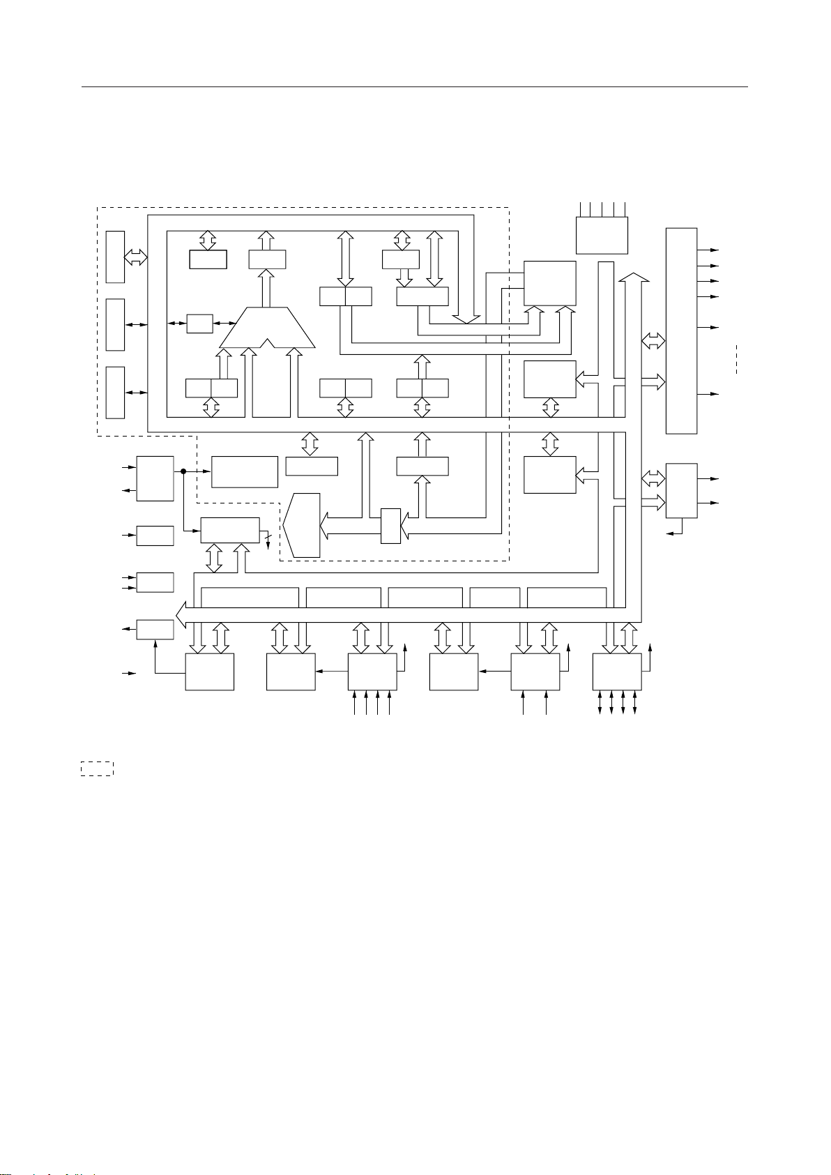
BLOCK DIAGRAM
SS3VSS2VSS1
C2C1V
BIAS
BSRHALTMIEF
TR2 TR0 TR1
(4)
PCM PCL
PCH
ROM
2528B
COM1
COM2
COM3
COM4
OSC0
OSC1
RESET
TST1
TST2
V
SSL
V
DD
OSC
RST
TST
VR
C
BA HL XY
ALU
(4) (4)
TIMING
CONTROLLER
TBC
A8 to A11
A7 to A0
PORT ADDRESS
RAM
128N
DB7 to DB0
ROMRSP
3
IR
IR
(8)
INTC
(8)
DECODER
INT
PORT ADDRESS
DB7 to DB0
BUP CAPR PORT2 EVENT PORT3 PORT6
INTINTINT
INT
LCD
MD0
SEG0
SEG35
MD0
MD0
is the CPU core (nX-4/20).
P2.0
P2.1
P2.2
P2.3
P3.0
P3.1
P6.0
P6.1
P6.2
P6.3
2/25
Page 3
¡ Semiconductor MSM64158A/64158AL
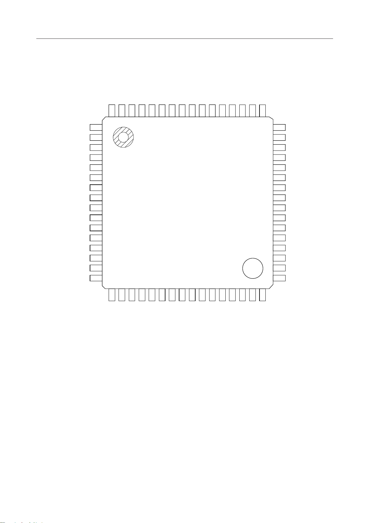
PIN CONFIGURATION (TOP VIEW)
SEG24
SEG25
SEG26
SEG27
SEG28
SEG29
SEG30
SEG31
SEG32
SEG33
SEG34
64
63
62
61
60
59
58
57
56
55
54
53 SEG35
52 MD0
51 MD0
50 TST1
49 TST2
SEG23
SEG22
SEG21
SEG20
SEG19
SEG18
SEG17
SEG16
SEG15
SEG14
SEG13
10
11
12SEG12
13SEG11
14SEG10
15SEG9
16SEG8
1
2
3
4
5
6
7
8
9
48
47
46
45
44
43
42
41
40
39
38
P6.0
P6.1
P6.2
P6.3
V
DD
P2.0
P2.1
P2.2
P2.3
P3.0
P3.1
37 RESET
36 V
SSL
35 OSC1
34 OSC0
33 V
SS1
17
18
19
20
21
22
23
24
25
26
27
28COM1
29C2
30C1
31V
32V
SEG7
SEG6
SEG5
SEG4
SEG3
SEG2
SEG1
SEG0
64-Pin Plastic QFP
COM4
COM3
COM2
SS3
SS2
3/25
Page 4
¡ Semiconductor MSM64158A/64158AL
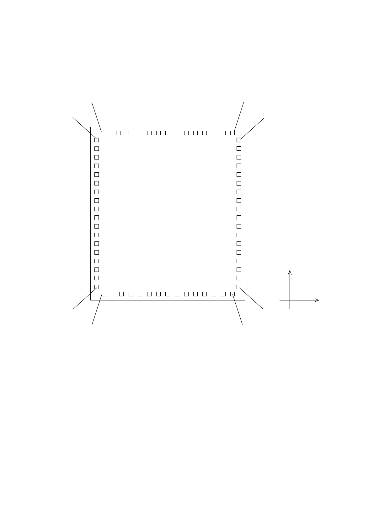
PAD CONFIGURATION
Pad Layout
47
46
33
32
Y
X
1564
1
14
Chip Size : 3.63 mm ¥ 3.99 mm
Chip Thickness : 350 mm (typ.)
Coordinate Origin : Chip center
Pad Hole Size : 110 mm ¥ 110 mm
Pad Size : 120 mm ¥ 120 mm
Minimum Pad Pitch : 180 mm
Note: The chip substrate voltage is VDD.
4/25
Page 5
¡ Semiconductor MSM64158A/64158AL
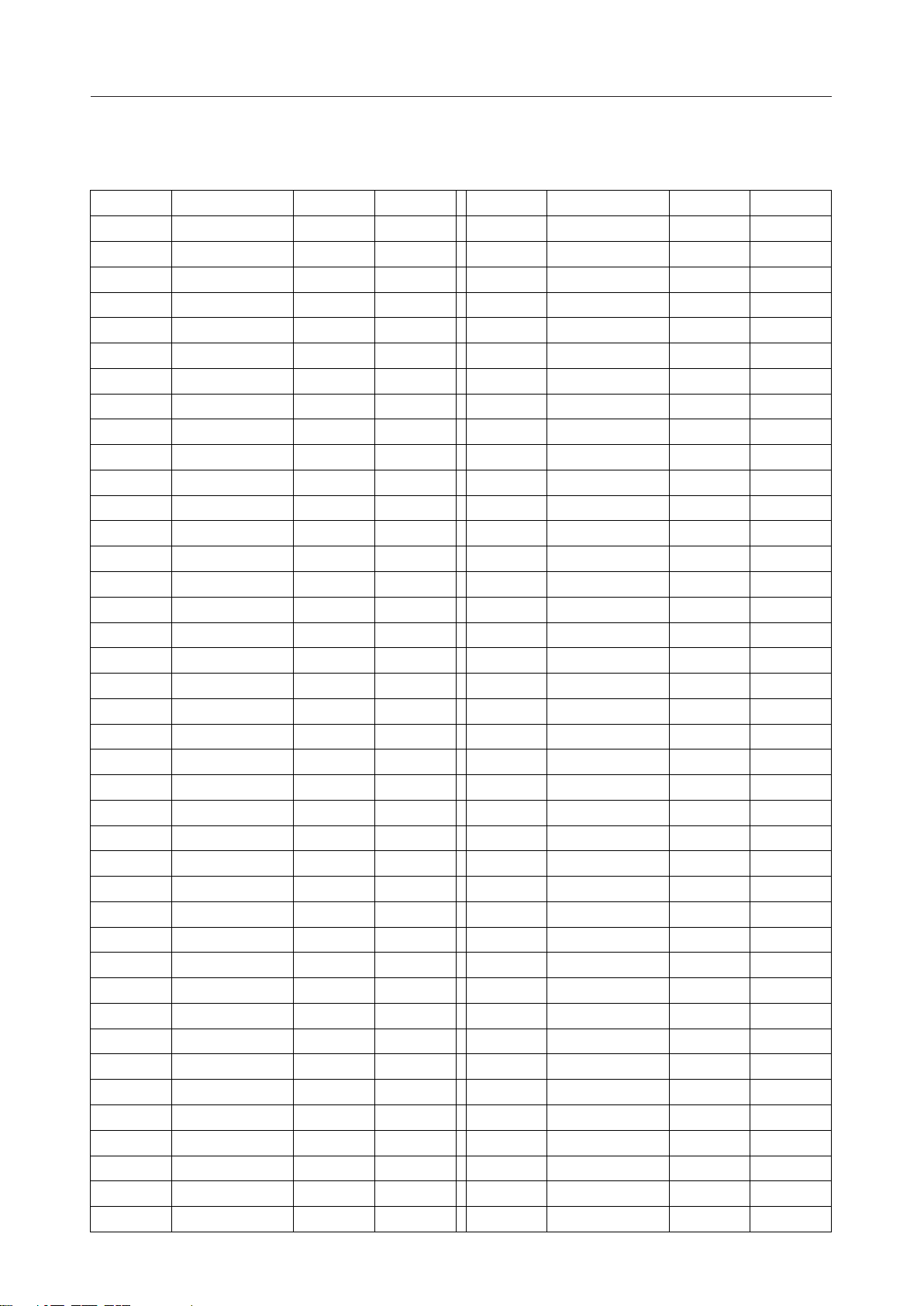
Pad Coordinates
Pad No. Y (µm)X (µm)Pad Name
1 –1794–1344MD0
2 MD0
3 SEG35
4
5
6
7
8
9
10
11
12
13
14
15
16
17
18 –1095
19 –891
20
21
22
23
24
25
26
27
28
29
30
31
32
33
34
35
36 844
37 657
38 471
39 285
SEG34
SEG33
SEG32
SEG31
SEG30
SEG29
SEG28
SEG27
SEG26
SEG25
SEG24
SEG23
SEG22
SEG21
SEG20
SEG19
SEG18
SEG17
SEG16
SEG15
SEG14
SEG13
SEG12
SEG11
SEG10
SEG9
SEG8
SEG7
SEG6
SEG5
SEG4
SEG3
SEG2
SEG1
SEG0
COM4
–1008 –274
–824 –461
–639 –647
–453 –1019
–267
–82
104
289
475
660
846
1031
1216
1664
1664
1664
1664
1664
1664
1664
1664
1664
1664
1664
1664
1664
1664
1664
1664
1664
1664
1216
1030
40 98COM3
–1794
–1794
–1794
–1794
–1794
–1794
–1794
–1794
–1794
–1794
–1794
–1794
–1794
–1689
–1491
–1293
–699
–501
–303
–105
93
291
489
687
885
1083
1281
1479
1677
17941395
1794
1794
1794
1794
1794
1794
1794
Pad No.
41 1794–88COM2
42 COM1
43 C2
44
45
46
47
48
49
50
51
52
53
54
55
56
57
58
59
60
61
62
63
64
C1
V
SS3
V
SS2
SS1
OSC0
OSC1
V
SSL
RESET
P3.1
P3.0
P2.3
P2.2
P2.1
P2.0
V
DD
P6.3
P6.2
P6.1
P6.0
TST2
TST1
–1496
–1664V
–1664
–1664
–1664
–1664
–1664
–1664
–1664
–1664
–1664
–1664
–1664
–1664
–1664
–1664
–1664
–1664
–1664
Y (µm)X (µm)Pad Name
1794
1794
1794
1794
1794
1671
1473
1275
1077
879
681
475
285
87
–111
–309
–507
–705
–903
–1101
–1299
–1497
–1703
5/25
Page 6
¡ Semiconductor MSM64158A/64158AL
PIN DESCRIPTIONS
Basic Functions
Function SymbolPad Description
Pin
44
33
58 Digital power supply (0 V)
47 Digital negative power supply (for 1.5 V spec.)
V
DD
V
SS1
Type
—
—
Bias output for LCD drive (for 3.0 V spec.)
Power
Supply
Oscillation
32
31
30
29
36
34
35
50
46 Digital negative power supply (for 3.0 V spec.)
45 Bias output for LCD drive (–4.5 V)
50
V
SS2
—
Bias output for LCD drive (for 1.5 V spec.)
V
SS3
C144 Capacitor connection pins for LCD drive bias generation.
C243
V
SSL
OSC048 Clock oscillation input and output pins:
—
—
—
Negative power supply pin for internal logic
—
(An internally generated constant voltage is present at this pin.)
I
Either a crystal (32.768 kHz) and a capacitor (10 to 30 pF)
OSC149
TST164 Input pins for test.
are connected to these pins or a resistor (1 MW) is.
O
I
Test
49
37
TST263
RESET51 System reset input pin:
I
I
Setting this pin to "H" level puts this device into a reset state.
Reset
Then, setting this pin to "L" level starts executing an instruction
from address 000H.
This pin is internally connected to V
down resistor.
SS1
or V
through a pull-
SS2
6/25
Page 7
¡ Semiconductor MSM64158A/64158AL
Basic Functions (continued)
Function Symbol Type Description
Ports
Melody
Drivers
Pin
43
42
41
40
39
38
48
47
46
45
51
52
28
Pad
57
56
55
54
53
52
62
61
60
59
1
2
42
P2.0 I 4-bit input port (port 2): Select between pull-down resistor
P2.1
P2.2
P2.3
P3.0
P3.1
P6.1
P6.2
P6.3
MD0 O
MD0 O
COM1 O
input and high impedance input for each bit with the port 2 control
register (P2CON). When configured for secondary function,
an external interrupt and capture circuit trigger input are allocated.
If P2.0 to P2.3 are all set to a "H" level, the device enters system
reset mode.
I
2-bit input port (port 3): Select between pull-down resistor input and
high impedance input with the port 3 control register (P3CON).
When configured for secondary function, an external interrupt is
allocated to P3.0 and an event counter input is allocated to P3.1.
I/OP6.0
4-bit I/O port (port 6): Select between input and output, between
pull-down resistor input and high impedance input, and between
open drain output and CMOS output with the port 6 control
register (P6CON).
When configured for secondary function, an external interrupt
is allocated to these pins.
Output pin of melody driver 0.
Inverted output pin of MD0 output.
LCD common signal output pins.
LCD
Drivers
27
26
25
41
40
39
COM2 O
COM3 O
COM4 O
7/25
Page 8
¡ Semiconductor MSM64158A/64158AL
Basic Functions (continued)
LCD
Drivers
PadPin
3824
Symbol
SEG0
SEG1
SEG2
SEG3
SEG4
SEG5
SEG6
SEG7
SEG8
SEG9
SEG10
SEG11
SEG12
SEG13
SEG14
SEG15
SEG16
SEG17
SEG18
SEG19
SEG20
SEG21
TypeFunction
O
LCD segment signal output pins.
O3723
O3622
O3521
O3420
O3319
O3218
O3117
O3016
O2915
O2814
O2713
O2612
O2511
O2410
O239
O228
O217
O206
O195
O184
O173
Description
SEG22
SEG23
SEG24
SEG25
SEG26
SEG27
1060
SEG28
SEG29
SEG30
SEG31
SEG32
SEG33
SEG34
SEG35
O162
O151
O1464
O1363
O1262
O1161
O
O959
O858
O757
O656
O555
O454
O353
8/25
Page 9

¡ Semiconductor MSM64158A/64158AL
Secondary Functions
External
Interrupts
Counter
Input
PadPin DescriptionTypeFunction
5743
5642
5541
5440
5339
6248
6147
6046
5945
5238Event
Symbol
P2.0
P2.1
P2.2
P2.3
P3.0
P6.0
P6.1
P6.2
P6.3
P3.1
I
P2.0 to P2.3 secondary functions :
These are level-triggered external interrupt input pins.
Select interrupt enable/disable for each bit with the
P2 interrupt enable register (P2IE).
If P2.0 to P2.3 pins are set to "H" level for a minimum
of 2 seconds, the device enters system reset mode.
P2.0, P2.1 secondary functions :
trigger input pins for capture circuit.
I
P3.0 secondary function :
This is an input pin for external interrupt. This pin can
receive an interrupt at a rising edge, a falling edge, or at
both rising and falling edges.
I
P6.0 to P6.3 secondary functions :
These are level-triggered external interrupt input pins.
I
P3.1 secondary function :
Input port for event counter
9/25
Page 10

¡ Semiconductor MSM64158A/64158AL
Handling When Specific Pins Are Not Used
Symbol
TST1 to TST2
P2.0 to P2.3
P3.0, P3.1
P6.0 to P6.3
MD0, MD0
COM1 to COM4
SEG0 to SEG35
Recommended Pin Connection
Open
"L" level or open
"L" level or open
In input mode : "L" level or open (Initial setting: input mode)
In output mode : Open
Open
Open
Open
10/25
Page 11

¡ Semiconductor MSM64158A/64158AL
ABSOLUTE MAXIMUM RATINGS
1.5 V Spec. (MSM64158A)
= 0 V)
(V
DD
Parameter
Power Supply Voltage 1
Power Supply Voltage 2
Power Supply Voltage 3
Power Supply Voltage 4
Input Voltage 1
Input Voltage 2
Output Voltage 1
Output Voltage 2
Output Voltage 3
Output Voltage 4
Storage Temperature
Symbol Condition Unit
V
V
V
V
V
V
V
V
T
SS1
SS2
SS3
SSL
V
IN1
V
IN2
OUT1
OUT2
OUT3
OUT4
STG
Ta = 25°C
Ta = 25°C
Ta = 25°C
Ta = 25°C
input, Ta = 25°C
V
SS1
input, Ta = 25°C
V
SSL
V
output, Ta = 25°C
SS1
output, Ta = 25°C
V
SS2
V
output, Ta = 25°C
SS3
output, Ta = 25°C
V
SSL
—
Rating
–2.0 to +0.3
–4.0 to +0.3
–5.5 to +0.3
–2.0 to +0.3
– 0.3 to +0.3
V
SS1
– 0.3 to +0.3
V
SSL
V
– 0.3 to +0.3
SS1
– 0.3 to +0.3
V
SS2
V
– 0.3 to +0.3
SS3
– 0.3 to +0.3
V
SSL
–55 to +150
V
V
V
V
V
V
V
V
V
V
°C
RECOMMENDED OPERATING CONDITIONS
1.5 V Spec. (MSM64158A)
Parameter
Operating Temperature
Operating Voltage
Crystal Oscillation Frequency
External RC Oscillator Resistance R
Symbol
T
op
V
SS1
f
XT
OS
—
BUPF = "0"
—
—
(V
DD
Range
–40 to +70
–1.7 to –1.25
–1.7 to –1.15BUPF = "1"
30 to 35 kHz
1 M ±10% W
= 0 V)
UnitCondition
°C
V
11/25
Page 12

¡ Semiconductor MSM64158A/64158AL
ELECTRICAL CHARACTERISTICS
1.5 V Spec. (MSM64158A)
DC Characteristics
= 0 V, V
(V
DD
Parameter Symbol Condition Min. Typ. Max. Unit
Ca, Cb, C12 = 0.1 mF
Ta = –40 to +60°C
BUPF = "0"
Ca, Cb, C12 = 0.1 mF
Ta = –40 to +70°C
BUPF = "0"
V
SS2
Voltage
V
SS2
Ca, Cb, C12 = 0.1 mF
Ta = –40 to +60°C
BUPF = "1"
Ca, Cb, C12 = 0.2 mF
Ta = –40 to +70°C
BUPF = "1"
Ca, Cb, C12 = 0.1 mF
Ta = –40 to +60°C
BUPF = "0"
C
, Cb, C12 = 0.1 mF
a
Ta = –40 to +70°C
BUPF = "0"
Voltage
V
SS3
V
SS3
Ca, Cb, C12 = 0.1 mF
Ta = –40 to +60°C
BUPF = "1"
Ca, Cb, C12 = 0.2 mF
Ta = –40 to +70°C
BUPF = "1"
BUPF = "0"
V
Voltage
SSL
Crystal Oscillation
Start Voltage
V
SSL
BUPF = "1"
V
Oscillation start time: within 5 seconds
STA
Crystal Oscillation
V
Hold Voltage
HOLD
External Crystal
C
Oscillator Capacitance
G
Internal Crystal
C
OscillatorCapacitance
D
RC Oscillation
Frequency
f
CR
ROS = 1 MW
= –1.5 V, Ta = –40 to +70°C unless otherwise specified.)
SS1
+100%
–20%
–3.2
–3.0
–2.8
+100%
–20%
+100%
–20%
–3.2
–3.2
–3.0
–3.0
–2.7
V
–2.5
+100%
–20%
–3.2
–3.0
–2.3
+100%
–20%
–4.7
–4.5
–4.2
+100%
–20%
+100%
–20%
–4.7
–4.7
–4.5
–4.5
–4.0
V
–3.9
+100%
–20%
–4.7
–1.5
–4.5
–1.3
–3.7
–0.6
V
–0.6
–1.3
–1.9
—
—
—
—
—
10
10
—
—
—
15
–1.45
–1.15
30
20
V
V
pF
pF
15 40 75 kHz
Measuring
Circuit
1, 1'
1
1'
12/25
Page 13

¡ Semiconductor MSM64158A/64158AL
DC Characteristics (continued)
• 32.768 kHz crystal oscillation
(V
= 0 V, V
DD
Parameter Symbol Condition Min. Typ. Max. Unit
CPU in halt state
Supply Current 1
I
DD1
BUPF = "0"
CPU in halt state
Supply Current 1
I
DD1
BUPF = "1"
CPU in operation
Supply Current 2
I
DD2
BUPF = "0"
CPU in operation
Supply Current 2
I
DD2
BUPF = "1"
= –1.5 V, Ta = –40 to +70°C unless otherwise specified.)
SS1
Measuring
Circuit
Ta = –40 to +40°C
Ta = +40 to +70°C
Ta = –40 to +40°C
Ta = +40 to +70°C
Ta = –40 to +40°C
Ta = +40 to +70°C
Ta = –40 to +40°C
Ta = +40 to +70°C
—
—
—
—
—
—
—
—
2.0
6.0
2.0
40
3.0
3.0
50
6.0
15
6.01050
10
25
10
60
mA
mA
mA
mA
mA
mA
mA
mA
1
• RC oscillation
(V
= 0 V, V
DD
Parameter Symbol Condition Min. Typ. Max. Unit
CPU in halt state
Supply Current 1
I
DD1
BUPF = "0"
CPU in halt state
Supply Current 1
I
DD1
BUPF = "1"
CPU in operation
Supply Current 2
I
DD2
BUPF = "0"
CPU in operation
Supply Current 2
I
DD2
BUPF = "1"
= –1.5 V, ROS = 1 MW, Ta = –40 to +70°C unless otherwise specified.)
SS1
Ta = –40 to +40°C
Ta = +40 to +70°C
Ta = –40 to +40°C
Ta = +40 to +70°C
Ta = –40 to +40°C
Ta = +40 to +70°C
Ta = –40 to +40°C
Ta = +40 to +70°C
—
—
—
—
—
—
—
—
3.0
3.0
6.0
6.0
7.0
7.01550
15
15
10
45
50
20
30
70
Measuring
mA
mA
mA
mA
mA
mA
mA
mA
Circuit
1'
13/25
Page 14

¡ Semiconductor MSM64158A/64158AL
DC Characteristics (continued)
(V
= 0 V, V
DD
Parameter
(Pin Name)
Output Current 1
(MD0, MD0)
Output Current 2
(SEG0 to SEG35)
(COM1 to COM4)
Output Current 3
(P6.0 to P6.3)
Output Leakage
Current
(P6.0 to P6.3)
= V
SS1
= –1.5 V, V
SSL
= –3.0 V, V
SS2
= –4.5 V, Ta = –40 to +70°C unless otherwise specified.)
SS3
Symbol Condition Min. Typ. Max. Unit
I
OH1
I
I
OH2
I
OMH2
I
OMH2S
I
OML2
I
OML2S
I
I
OH3
I
I
OOH
I
OOL
OL1
OL2
OL3
V
= –0.5 V
OH1
= V
V
OL1
= –0.2 V
V
OH2
V
OMH2
V
OMH2S
V
OML2
V
OML2S
V
= V
OL2
V
= –0.5 V
OH3
V
= V
OL3
VOH = V
VOL = V
= V
= V
= V
= V
DD
SS1
SS1
SS1
SS2
SS3
SS1
+ 0.5 V
+ 0.2 V
– 0.2 V
SS1
+ 0.2 V
– 0.2 V
SS2
+ 0.2 V
+ 0.5 V
(V
(V
(V
(V
(V
(V
DD
SS1
SS1
SS2
SS2
SS3
level)
level)
level)
level)
level)
level)
–0.1
–0.6
–2.0
0.1 0.6 2.0 mA
–4.0
—
—
4.0
——
—
— –4.0
—
—
4.0
— — –4.0 mA
4.0 — — mA
–5.0 –2.1 –0.3 mA
0.1 0.7 2.0 mA
— — 0.3 mA
–0.3 — — mA
Measuring
Circuit
mA
mA
mA
mA
mA
2
Input Current 1
(P2.0 to P2.3)
(P3.0, P3.1)
(P6.0 to P6.3)
Input Current 2
(TST1, TST2)
Input Current 3
(RESET)
Input Voltage 1
(P2.0 to P2.3)
(P3.0, P3.1)
(P6.0 to P6.3)
(TST1, TST2)
(RESET)
I
I
IH1Z
I
I
I
I
I
V
V
IH1
IL1
IH2
IL2
IH3
IL3
IH1
IL1
V
= V
IH1
DD
= V
V
IH1
DD
V
= V
IL1
SS1
V
= V
IH2
DD
V
= V
IL2
SS1
V
= V
IH3
DD
V
= V
IL3
SS1
(when pulled down)
(in a high-impedance state)
—
1.0
100
mA
0 — 1.0 mA
–1.0
0.3
—0
0.75 1.5
–1.020—
mA
mA
0
mA
1.0 10 100 mA
–1.0 — 0 mA
–0.3 — 0 V
3
4
—
–1.5 — –1.2 V
14/25
Page 15

¡ Semiconductor MSM64158A/64158AL
Measuring circuit 1
V
SSL
C
L
Measuring circuit 1'
OSC1
Crystal
32.768 kHz
V
DD
C
G
OSC0
MSM64158A
C1
C
12
C2
V
DD
AV V V
V
SS1VSS2
C
V
SS3
Ca, Cb, C
C
a
b
C
C
12
L
G
: 0.1 to 0.2 mF
: 0.1 mF
: 15 pF
OSC1
R
OS
OSC0
MSM64158A
C1
C
12
V
SSL
V
C
L
DD
V
SS1VSS2
C
V
SS3
a
C
b
V VAV
C2
Ca, Cb, C
C
L
R
OS
12
: 0.1 to 0.2 mF
: 0.1 mF
: 1 MW
15/25
Page 16

¡ Semiconductor MSM64158A/64158AL
Measuring circuit 2
(*2)
V
IH
(*1)
V
IL
Measuring circuit 3
INPUT
V
DD
MSM64158A
V
SS1VSS2VSS3VSSL
A
OUTPUT
(*3)
A
MSM64158A
INPUT
V
DD
V
SS1VSS2VSS3VSSL
OUTPUT
16/25
Page 17

¡ Semiconductor MSM64158A/64158AL
Measuring circuit 4
V
IH
V
SS1
MSM64158A
V
SS2VSS3VSSL
(*3)
V
IL
INPUT
V
DD
*1 Input logic circuit to determine the specified measuring conditions.
*2 Measured at the specified output pins.
*3 Measured at the specified input pins.
Waveform
Monitoring
OUTPUT
17/25
Page 18

¡ Semiconductor MSM64158A/64158AL
ABSOLUTE MAXIMUM RATINGS
3.0 V Spec. (MSM64158AL)
= 0 V)
(V
DD
Power Supply Voltage 1
Power Supply Voltage 2
Power Supply Voltage 3
Power Supply Voltage 4
Input Voltage 1
Input Voltage 2
Output Voltage 1
Output Voltage 2
Output Voltage 3
Storage Temperature
Symbol Condition Unit
V
V
V
V
V
V
V
V
V
T
SS1
SS2
SS3
SSL
IN1
IN2
OUT1
OUT2
OUT3
STG
Ta = 25°C
Ta = 25°C
Ta = 25°C
Ta = 25°C
input, Ta = 25°C
V
SS2
V
input, Ta = 25°C
SSL
output, Ta = 25°C
V
SS2
output, Ta = 25°C
V
SS3
V
output, Ta = 25°C
SSL
—
RatingParameter
–2.0 to +0.3
–4.0 to +0.3
–5.5 to +0.3
–4.0 to +0.3
– 0.3 to +0.3
V
SS2
V
– 0.3 to +0.3
SSL
– 0.3 to +0.3
V
SS2
– 0.3 to +0.3
V
SS3
V
– 0.3 to +0.3
SSL
–55 to +150
V
V
V
V
V
V
V
V
V
°C
RECOMMENDED OPERATING CONDITIONS
3.0 V Spec. (MSM64158AL)
Symbol Condition Unit
Operating Temperature
Operating Voltage
Crystal Oscillation Frequency f
External RC Oscillator Resistance R
T
op
V
SS2
XT
OS
—
BUPF = "0"
BUPF = "1"
—
—
(V
DD
RangeParameter
–40 to +70
–3.5 to –2.5
–3.5 to –2.0
30 to 66 kHz
1 M ±10% W
= 0 V)
°C
V
18/25
Page 19

¡ Semiconductor MSM64158A/64158AL
ELECTRICAL CHARACTERISTICS
3.0 V Spec. (MSM64158AL)
DC Characteristics
(V
= 0 V, V
DD
Parameter Symbol Condition Min. Typ. Max. Unit
= –3.0 V, Ta = –40 to +70°C unless otherwise specified.)
SS2
Measuring
Circuit
V
Voltage
SS1
Voltage
V
SS3
Voltage
V
SSL
Crystal Oscillation
Start Voltage
Crystal Oscillation
Hold Voltage
External Crystal
Oscillator Capacitance
Internal Crystal
Oscillator Capacitance
RC Oscillation
Frequency
V
V
V
V
V
SS1
SS3
SSL
STA
HOLD
C
G
C
D
f
CR
Ca, Cb, C12 = 0.1 mF
, Cb, C12 = 0.1 mF
C
a
+100%
–20%
+100%
–20%
BUPF = "0"
BUPF = "1"
Oscillation start time: within 5 seconds
—
—
—
= 1 MW
R
OS
–1.7 –1.5 –1.3
–4.7 –4.5 –4.2 V
–1.5 –1.3 –0.6
–1.9 –1.3 –0.6
—
— — –2.0 V
10 — 30 pF
10 15 20 pF
15 40 75 kHz
V
1
1'
V
V— –2.5
1
1'
19/25
Page 20

¡ Semiconductor MSM64158A/64158AL
DC Characteristics (continued)
• 32.768 kHz crystal oscillation
(V
= 0 V, V
DD
Parameter Symbol Condition Min. Typ. Max. Unit
CPU in halt state
Supply Current 1
I
DD1
BUPF = "0"
CPU in halt state
Supply Current 1
I
DD1
BUPF = "1"
CPU in operation
Supply Current 2
I
DD2
BUPF = "0"
CPU in operation
Supply Current 2
I
DD2
BUPF = "1"
= –3.0 V, Ta = –40 to +70°C unless otherwise specified.)
SS2
Measuring
Circuit
Ta = –40 to +40°C
Ta = +40 to +70°C
Ta = –40 to +40°C
Ta = +40 to +70°C
Ta = –40 to +40°C
Ta = +40 to +70°C
Ta = –40 to +40°C
Ta = +40 to +70°C
—
—
—
—
—
—
—
—
0.9
0.9
1.5
1.5
3.0
3.0
5.0
5.0
4.5
30
6.0
40
10
40
15
50
mA
mA
mA
mA
mA
mA
mA
mA
1
• RC oscillation
= 0 V, V
(V
DD
Parameter Symbol Condition Min. Typ. Max. Unit
CPU in halt state
Supply Current 1
I
DD1
BUPF = "0"
CPU in halt state
Supply Current 1
I
DD1
BUPF = "1"
CPU in operation
Supply Current 2
I
DD2
BUPF = "0"
CPU in operation
Supply Current 2
I
DD2
BUPF = "1"
= –3.0 V, ROS = 1 MW, Ta = –40 to +70°C unless otherwise specified.)
SS2
Ta = –40 to +40°C
Ta = +40 to +70°C
Ta = –40 to +40°C
Ta = +40 to +70°C
Ta = –40 to +40°C
Ta = +40 to +70°C
Ta = –40 to +40°C
Ta = +40 to +70°C
—
—
—
—
—
—
—
—
1.5
1.5
3.0
3.0
4.0
4.01050
8.0
8.0
6.0
40
50
12
25
60
Measuring
mA
mA
mA
mA
mA
mA
mA
mA
Circuit
1
20/25
Page 21

¡ Semiconductor MSM64158A/64158AL
DC Characteristics (continued)
(VDD = 0 V, V
Parameter
(Pin Name)
Output Current 1
(MD0, MD0)
Output Current 2
(SEG0 to SEG35)
(COM1 to COM4)
Output Current 3
(P6.0 to P6.3)
Output Leakage
Current
(P6.0 to P6.3)
Input Current 1
(P2.0 to P2.3)
(P3.0, P3.1)
(P6.0 to P6.3)
Input Current 2
(TST1, TST2)
Input Current 3
(RESET)
Input Voltage 3
(P2.0 to P2.3)
(P3.0, P3.1)
(P6.0 to P6.3)
(TST1, TST2)
(RESET)
= V
SS1
= –1.5 V, V
SSL
= –3.0 V, V
SS2
= –4.5 V, Ta = –40 to +70°C unless otherwise specified.)
SS3
Symbol Condition Min. Typ. Max. Unit
I
OH1
I
OL1
I
OH2
I
OMH2
I
OMH2S
I
OML2
I
OML2S
I
OL2
I
OH3
I
OL3
I
OOH
I
OOL
I
IH1
I
IH1Z
I
I
IH2
I
I
IH3
I
V
V
IL1
IL2
IL3
IH1
IL1
V
= –0.5 V
OH1
= V
V
OL1
= –0.2 V
V
OH2
V
OMH2
V
OMH2S
V
OML2
V
OML2S
V
= V
OL2
= –0.5 V
V
OH3
V
= V
OL3
VOH = V
VOL = V
V
= V
IH1
V
= V
IH1
V
= V
IL1
V
= V
IH2
V
= V
IL2
V
= V
IH3
V
= V
IL3
= V
= V
= V
= V
DD
SS2
DD
DD
SS2
DD
SS2
DD
SS2
SS2
SS1
SS2
SS2
SS3
SS2
+ 0.5 V
(V
level)
DD
+ 0.2 V
– 0.2 V
SS1
+ 0.2 V
– 0.2 V
+ 0.2 V
(V
(V
(V
(V
(V
SS1
SS1
SS2
SS2
SS3
level)
level)
level)
level)
level)
+ 0.5 V
(when pulled down)
(in a high-impedance state)
—
—
–6.0
–1.8
–0.7
0.7 1.8 6.0 mA
—
—
–.04
4.0
——
—
— –4.0
4.0
—
—
— — –4.0 mA
4.0 — — mA
–18 –6.0 –2.0
0.7 1.6 6.0 mA
— — 0.3 mA
–0.3 — — mA
50
100—300
0 — 1.0 mA
–1.0
0.75
–1.0
—0
1.5 3.0
0
20 40 200 mA
–1.0 — 0 mA
–0.6 — 0 V
–3.0 — –2.4 V
Measuring
Circuit
mA
mA
mA
mA
mA
2
mA
mA
mA
3
mA
mA
4
21/25
Page 22

¡ Semiconductor MSM64158A/64158AL
Measuring circuit 1
C
L
Measuring circuit 1'
OSC1
Crystal
32.768 kHz
V
DD
C
G
OSC0
MSM64158AL
C1
C
12
V
SSL
V
DD
V
SS2VSS1
C
V
SS3
C
a
b
AV V V
C2
Ca, Cb, C12, C
C
G
L
: 0.1 µF
: 15 pF
OSC1
R
OS
OSC0
MSM64158AL
C1
C
12
V
SSL
V
C
L
DD
V
SS2VSS1
C
V
SS3
a
C
b
V VAV
C2
Ca, Cb, C12, C
R
OS
L
: 0.1 mF
:1 MW
22/25
Page 23

¡ Semiconductor MSM64158A/64158AL
Measuring circuit 2
(*2)
V
IH
(*1)
V
IL
Measuring circuit 3
A
(*3)
INPUT
V
DD
MSM64158AL
V
SS1
V
SS2VSS3
A
OUTPUT
V
SSL
INPUT
V
DD
MSM64158AL
V
SS1VSS2VSS3VSSL
OUTPUT
23/25
Page 24

¡ Semiconductor MSM64158A/64158AL
Measuring circuit 4
V
IH
(*3)
V
IL
INPUT
V
DD
MSM64158AL
V
SS1
V
SS2VSS3VSSL
*1 Input logic circuit to determine the specified measuring conditions.
*2 Measured at the specified output pins.
*3 Measured at the specified input pins.
Waveform
Monitoring
OUTPUT
24/25
Page 25

¡ Semiconductor MSM64158A/64158AL
PACKAGE DIMENSIONS
(Unit : mm)
QFP64-P-1414-0.80-BK
Mirror finish
Package material
Lead frame material
Pin treatment
Solder plate thickness
Package weight (g)
Epoxy resin
42 alloy
Solder plating
5 mm or more
0.87 TYP.
Notes for Mounting the Surface Mount Type Package
The SOP, QFP, TSOP, SOJ, QFJ (PLCC), SHP and BGA are surface mount type packages, which
are very susceptible to heat in reflow mounting and humidity absorbed in storage.
Therefore, before you perform reflow mounting, contact Oki’s responsible sales person for the
product name, package name, pin number, package code and desired mounting conditions
(reflow method, temperature and times).
25/25
 Loading...