

Datasheet MSM64155A-xxx, MSM64155AL-xxx, MSM64155AL-xxxGS-BK, MSM64155A-xxxGS-BK Datasheet (OKI)
Page 1

E2E0030-38-95
This version: Sep. 1998
MSM64155A/64155AL¡ Semiconductor
¡ Semiconductor
Previous version: Mar. 1996
MSM64155A/64155AL
4-Bit Microcontroller with Built-in LCD Driver and Melody Circuit
GENERAL DESCRIPTION
The MSM64155A (1.5 V)/64155AL (3.0 V) is a high-performance 4-bit microcontroller that
incorporates Oki-original CPU core nX-4/20.
The MSM64155A/64155AL has an LCD driver for up to 240 segments, an event counter, and
melody circuits. It is best suited for applications such as clocks and LCD games.
FEATURES
• Operating range
Operating voltage : 1.5 V/3.0 V
Operating temperature : –40 to +70 °C
Operating frequency : 32.768 kHz crystal oscillation
Approx. 32 kHz RC oscillation
Supply current (Typ.) : 0.9 mA (3.0 V at HALT mode)
• Minimum instruction execution time : 91 ms
• General memory space : 4064 bytes
• Local memory space : 256 nibbles
• LCD driver : 64
Common driver ¥ 4
Segment driver ¥ 60
1/4 duty, 1/3 bias; 240 segments (60 ¥ 4)
1/3 duty, 1/3 bias; 180 segments (60 ¥ 3)
• I/O port
Input-output port : 2 ports ¥ 4 bits (open-drain output/CMOS output
selectable; pull-down resistor input/high-impedance
input selectable)
Input port :
Output port : 1 port ¥ 4 bits (CMOS output)
• Event counter : 1 channel
• Melody output : 2
• Interrupts : 10 sources
• Package:
100-pin plastic QFP (QFP100-P-1420-0.65-BK) : (Product name : MSM64155A-¥¥¥GS-BK,
Chip : MSM64155A-¥¥¥, MSM64155AL-¥¥¥
• OTP version (for program evaluation) : MSM64P155/64P155L
(The power polarity and operating voltage of the MSM64P155/64P155L are different from the
MSM64155A/64155AL. For details, refer to the "MSM64P155 User's Manual".)
1 port ¥ 2 bits (pull-down resistor input/high-impedance
input selectable
1 port ¥ 4 bits (pull-down resistor input/high-impedance
input selectable)
External 4, time base 4, melody 2
¥¥¥ indicates a code number.
)
MSM64155AL-¥¥¥GS-BK)
1/26
Page 2
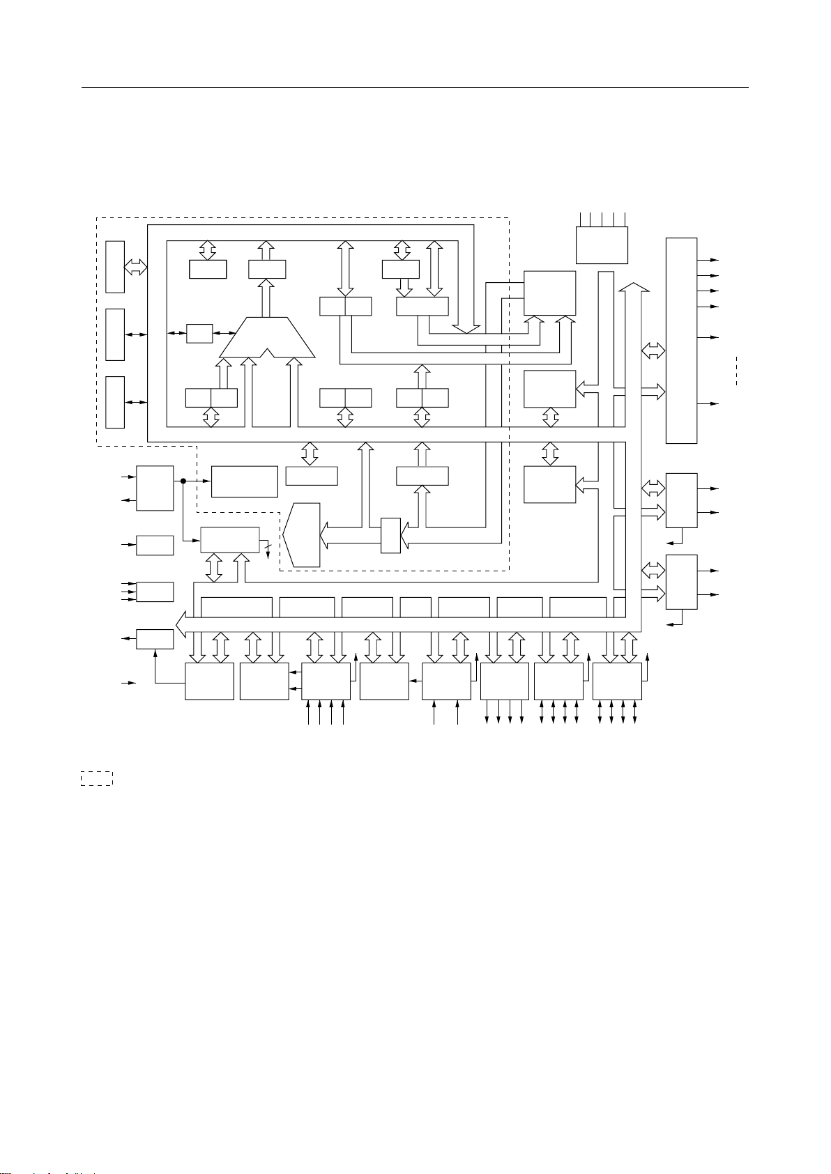
BLOCK DIAGRAM
BSRHALTMIEF
TR2 TR0 TR1
(4)
PCM PCL
PCH
ROM
4064B
MSM64155A/64155AL¡ Semiconductor
C2C1V
BIAS
SS3VSS2VSS1
COM1
COM2
COM3
COM4
OSC0
OSC1
RESET
TST1
TST2
TST3
V
SSL
V
DD
CLK
RST
TST
VR
C
BA HL XY
ALU
(4) (4)
TIMING
CONTROLLER
TBC
A8 to A11
A7 to A0
PORT ADDRESS
RAM
256N
DB7 to DB0
ROMRSP
4
IR
IR
(8)
INTC
(8)
DECODER
INT
PORT ADDRESS
DB7 to DB0
INT INTINTINT
BUP CAPR PORT2 EVENT PORT3 PORT4 PORT6 PORT7
INT
INT
LCD
MD0
MD1
SEG0
SEG59
MD0
MD0
MD1
MD1
is the CPU core (nX-4/20).
P2.0
P2.1
P2.2
P2.3
P3.0
P3.1
P4.0
P4.1
P4.2
P4.3
P6.0
P6.1
P6.2
P6.3
P7.0
P7.1
P7.2
P7.3
2/26
Page 3
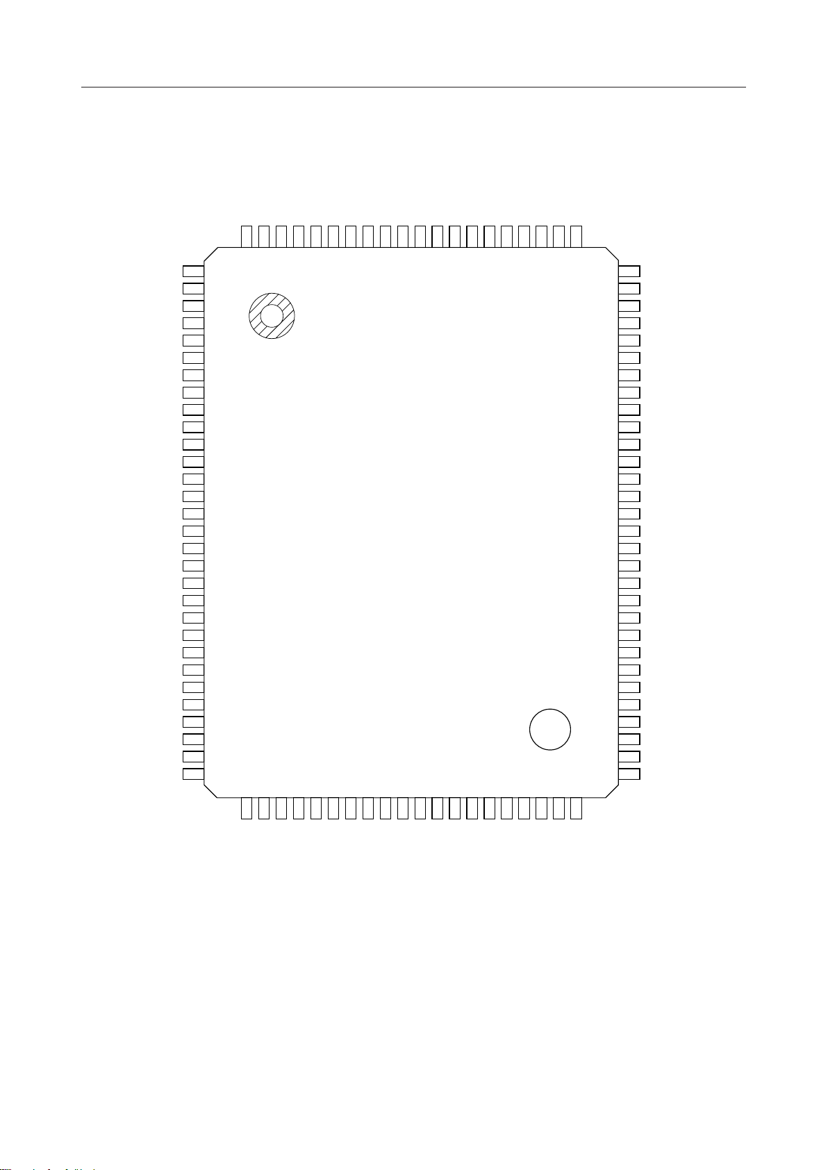
PIN CONFIGURATION (TOP VIEW)
SS3
SS2
SS1
V
100
C1
V
V
97
98
99
C2
96
COM2
COM1
94
95
COM4
COM3
92
93
SEG1
SEG0
90
91
SEG3
SEG2
88
89
SEG5
SEG4
86
87
SEG7
SEG6
84
85
SEG9
SEG8
82
83
MSM64155A/64155AL¡ Semiconductor
SEG10
81
RESET
OSC0
OSC1
V
SSL
P2.3
P2.2
P2.1
P2.0
P3.1
P3.0
P4.3
P4.2
P4.1
P4.0
P6.3
P6.2
P6.1
P6.0
P7.3
P7.2
P7.1
P7.0
V
DD
MD0
MD0
MD1
MD1
TST3
TST2
TST1
1
2
3
4
5
6
7
8
9
10
11
12
13
14
15
16
17
18
19
20
21
22
23
24
25
26
27
28
29
30
80
79
78
77
76
75
74
73
72
71
70
69
68
67
66
65
64
63
62
61
60
59
58
57
56
55
54
53
52
51
SEG11
SEG12
SEG13
SEG14
SEG15
SEG16
SEG17
SEG18
SEG19
SEG20
SEG21
SEG22
SEG23
SEG24
SEG25
SEG26
SEG27
SEG28
SEG29
SEG30
SEG31
SEG32
SEG33
SEG34
SEG35
SEG36
SEG37
SEG38
SEG39
SEG40
32
31
35
34
33
38
37
36
41
40
39
44
43
42
47
46
45
50
49
48
(NC)
SEG41
SEG42
SEG43
SEG44
SEG45
SEG46
SEG47
SEG48
SEG49
SEG50
SEG51
SEG52
SEG53
SEG54
SEG55
SEG56
SEG57
SEG58
SEG59
100-Pin Plastic QFP
Note: Pins marked as (NC) are no-connection pins which are left open.
3/26
Page 4
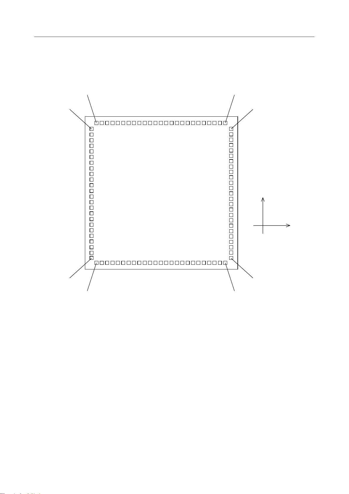
PAD CONFIGURATION
Pad Layout
MSM64155A/64155AL¡ Semiconductor
76
75
51
50
Y
X
251
Chip Size : 4.35 mm ¥ 4.50 mm
Chip Thickness : 350 mm (typ.)
Coordinate Origin : Chip center
Pad Hole Size : 110 mm ¥ 110 mm
Pad Size : 120 mm ¥ 120 mm
Minimum Pad Pitch : 150 mm
Note: The chip substrate voltage is VDD.
2699
4/26
Page 5

Pad Coordinates
MSM64155A/64155AL¡ Semiconductor
Pad No.
Pad
Name
X (µm) Y (µm)
1 OSC1 –1858 –2045
2 –1703
3 –1548
4 –1393
5 –1238
6 –1084
7 –929
8 –774
9 –619
10 –464
11 –310
12 –155
13 0
14 155
15 310
16 464
17 619
18 774
19 929
20 1084
21 1238
22 1430
V
SSL
P2.3
P2.2
P2.1
P2.0
P3.1
P3.0
P4.3
P4.2
P4.1
P4.0
P6.3
P6.2
P6.1
P6.0
P7.3
P7.2
P7.1
P7.0
V
DD
MD0
23 MD0 1658
24 MD1 1813
25 MD1 1968
26 TST3 2020
27 TST2 2020
28 TST1
29
SEG59
SEG58
30
31
SEG57
32
SEG56
33
SEG55
34
SEG54
35
SEG53
36
SEG52
37
SEG51
38
SEG50
39
SEG49
40
SEG48
2020
2020
2020
2020
2020
2020
2020
2020
2020
2020
2020
2020
2020
Pad No.
41 81
42
–2045
–2045
–2045
–2045
–2045
–2045
–2045
–2045
–2045
–2045
–2045
–2045
–2045
–2045
–2045
–2045
–2045
–2045
–2045
–2045
–2045
–2045
–2045
–1810
–1655
–1500
–1345
–1190
–1036
–881
–726
–571
–416
–262 –2020
–107 –2020
48 –2020
203 –2020
358 –2020
43
44
45
46
47
48
49
50
51
52
53
54
55
56
57
58
59
60
61
62
63
64
65
66
67
68
69
70
71
72
73
74
75
76
77
78
79
80
Pad
Name
SEG47
SEG46
SEG45
SEG44
SEG43 SEG3
SEG42
SEG41
SEG40
SEG39
SEG38
SEG37
SEG36
SEG35
SEG34
SEG33
SEG32
X (µm) Y (µm)
2020 512
2020
2020
2020
2020
2020
2020
2020
2020
2020
1780
1625
1471
1316
1161
1006
SEG31
SEG30
SEG29
SEG28
SEG27
SEG26
SEG25
SEG24
SEG23
SEG22
SEG21
SEG20
SEG19
SEG18
SEG17
SEG16
SEG15
SEG14
SEG13
–232
–387
–542
–697
–851
–1006
–1161
–1316
–1471
–1625
–1780
–1935
SEG12
SEG11
SEG10
SEG9
SEG8
851
697
542
387
232
77
–77
667
822
977
1132
1286
1441
1596
1751
1906
2045
2045
2045
2045
2045
2045
2045
2045
2045
2045
2045
2045
2045
2045
2045
2045
2045
2045
2045
2045
2045
2045
2045
2045
2045
1772
1617
1462
1307
1153
Pad No.
82
83
84
85
86
87
88
89
90
91
92
93
94
95
96
97
98
99
Pad
Name
SEG7
SEG6–2045
SEG5
SEG4
SEG2
SEG1
SEG0
COM4
COM3
COM2
COM1
C2
C1
V
SS3
V
SS2
V
SS1
RESET
OSC0
X (µm) Y (µm)
–2020 998
–2020
–2020
–2020
–2020
–2020
–2020
–2020
–2020
–2020
–2020
–2020
–2020
–2020
–2020
–2020
–2020
–2020
–2020
843
688
533
379
224
69
–86
–241
–395
–550
–705
–860
–1015
–1169
–1324
–1479
–1634
–1789
5/26
Page 6

PIN DESCRIPTIONS
Basic Functions
MSM64155A/64155AL¡ Semiconductor
Function
Power
Supply
Oscillation
Test
RESET
Pin
23
100
99
98
97
96
4
2
3
30
29
28
198 I
Pad
21
97
96
95
94
93
2
99
1
28
27
26
Symbol
V
DD
V
SS1
V
SS2
V
SS3
C1
C2
V
SSL
OSC0
OSC1
TST1
TST2
TST3
RESET
—
—
—
—
—
—
—
I
O
I
I
I
DescriptionType
Digital supply voltage (0 V)
Digital negative power supply (1.5 V spec.)
Bias output for LCD driver (3.0 V spec.)
Digital negative power supply (3.0 V spec.)
Bias output for LCD driver (1.5 V spec.)
Bias output for LCD driver (–4.5 V)
For connection to capacitors that generate bias for the
LCD driver
Negative power supply voltage pin for internal logic
(An internally generated constant voltage is present at this pin.)
Clock oscillation pins:
Either a crystal (32.768 kHz) and a capacitor (10 to 30 pF)
are connected to these pins or a resistor (1 MW) is.
Input pins for test
System reset input pin :
Setting this pin to "H" level puts this device into a reset state.
Then, setting this pin to "L" level starts executing an instruction
from address 000H.
This pin is internally connected to V
SS1
or V
through a
SS2
pull-down resistor.
6/26
Page 7
Basic Functions (continued)
MSM64155A/64155AL¡ Semiconductor
PadPin DescriptionTypeFunction
Ports 4-bit input port (port 2) :
7
6
53
10
9
13
12
11 9
17
16
15 13
68
5
4
8
7
1214
11
10
1618
15
14
Symbol
P2.0
P2.1
P2.2
P2.3
P3.0
P3.1
P4.0
P4.1
P4.2
P4.3
P6.0
P6.1
P6.2
P6.3
I
Select between pull-down resistor input and high impedance
input for each bit with the port 2 control register (P2CON).
When configured for secondary functions, an external
interrupt and capture circuit trigger input are allocated.
If P2.0 to P2.3 are set to "H" level, the device enters system
reset mode.
I 2-bit input port (port 3) :
Select between pull-down resistor input and high impedance
input with the port 3 control register (P3CON).
When configured for a secondary function, an external
interrupt is allocated to P3.0 and an event counter is
allocated to P3.1.
O
4-bit output port (port 4) :
4-bit CMOS output port.
4-bit input-output port (port 6) :
I/O
Select between input and output, between pull-down resistor
input and high impedance input, and between open-drain
output and CMOS output with the port 6 control register
(P6CON). When configured for a secondary function, an
external interrupt is allocated.
Melody
Drivers
LCD
Drivers
2022
21 19
20 18 P7.2
19 17
9295
94
93
92 89
91
90
P7.0
P7.1
P7.3
MD0
MD0
MD1
MD1
COM1
COM2
COM3
COM4
4-bit input-output port (port 7) :
I/O
Select between input and output, between pull-down
resistor input and high impedance input, and between
open-drain output and CMOS output with the port 7 control
register (P7CON). When configured for a secondary
function, an external interrupt is allocated.
O Output pin of melody driver 0.2325
O Inverted output pin of MD0 output.2224
O Output pin of melody driver 1.2426
O Inverted output pin of MD1 output.2527
O
LCD common signal output pins.
O
O
O
7/26
Page 8

Basic Functions (continued)
MSM64155A/64155AL¡ Semiconductor
LCD
Drivers
PadPin DescriptionTypeFunction
8891
Symbol
SEG0
SEG1
SEG2
SEG3
SEG4
SEG5
SEG6
SEG7
SEG8
SEG9
SEG10
SEG11
SEG12
SEG13
SEG14
SEG15
SEG16
O
LCD segment signal output pins.
O8790
O8689
O8588
O8487
O8386
O8285
O8184
O8083
O7982
O7881
O7780
O7679
O7578
O7477
O7376
O7275
SEG17
SEG18
SEG19
SEG20
SEG21
SEG22
SEG23
SEG24
SEG25
SEG26
SEG27
SEG28
SEG29
SEG30
SEG31
SEG32
SEG33
SEG34
O7174
O7073
O6972
O6871
O6770
O6669
O6568
O6467
O6366
O6265
O6164
O6063
O5962
O5861
O5760
O5659
O5558
O5457
SEG35
SEG36
SEG37
SEG38
SEG39
O5356
O5255
O5154
O5053
O4952
8/26
Page 9

Basic Functions (continued)
MSM64155A/64155AL¡ Semiconductor
LCD
Drivers
39
38
37
36
35
34
33
32
31
PadPin DescriptionTypeFunction
4851
Symbol
SEG40
SEG41
SEG42
SEG43
SEG44
SEG45
SEG46
SEG47
SEG48
SEG49
SEG50
SEG51
SEG52
SEG53
SEG54
SEG55
SEG56
SEG57
SEG58
SEG59
O
LCD segment signal output pins.
O4750
O4649
O4548
O4447
O4346
O4245
O4144
O4043
O3942
O3841
O37
O36
O35
O34
O33
O32
O31
O30
O29
9/26
Page 10

Secondary Functions
MSM64155A/64155AL¡ Semiconductor
External
Interrupts
PadPin DescriptionTypeFunction
68
57
46
35
810
1618
1517
1416
1315
2022
1921
1820
Symbol
P2.0
P2.1
P2.2
P2.3
P3.0
P6.0
P6.1
P6.2
P6.3
P7.0
P7.1
P7.2
I
P2.0 to P2.3 secondary functions :
These are level-triggered external interrupt input pins.
Select interrupt enable/disable for each bit with the
P2 interrupt enable register (P2IE).
If P2.0 to P2.3 pins are set to "H" level for a minimum
of 2 seconds, the device enters system reset mode.
P2.0, P2.1 secondary functions :
trigger input pins for capture circuit.
I
P3.0 secondary function :
This is an input pin for external interrupt. This pin can
receive an interrupt at a rising edge, a falling edge, or at
both rising and falling edges.
I
P6.0 to P6.3 secondary functions :
These are level-triggered external interrupt input pins.
I
P7.0 to P7.3 secondary functions :
These are level-triggered external interrupt input pins.
Counter
Input
1719
79Event
P7.3
P3.1
I
P3.1 secondary function :
Input port for event counter
10/26
Page 11

Handling When Specific Pins Are Not Used
MSM64155A/64155AL¡ Semiconductor
Symbol
TST1 to TST3
P2.0 to P2.3
P3.0, P3.1
P4.0 to P4.3
P6.0 to P6.3
P7.0 to P7.3
MD0, MD0
MD1, MD1
COM1 to COM4
SEG0 to SEG59
Recommended Pin Connection
Open
"L" level or open
"L" level or open
Open
In input mode : "L" level or open (Initial setting: input mode)
In output mode : Open
In input mode : "L" level or open (Initial setting: input mode)
In output mode : Open
Open
Open
Open
11/26
Page 12

ABSOLUTE MAXIMUM RATINGS
1.5 V Spec. (MSM64155A)
Parameter
Power Supply Voltage 1
Power Supply Voltage 2
Power Supply Voltage 3
Power Supply Voltage 4
Input Voltage 1
Input Voltage 2
Output Voltage 1
Output Voltage 2
Output Voltage 3
Output Voltage 4
Storage Temperature
Symbol Condition Unit
V
SS1
V
SS2
V
SS3
V
SSL
V
IN1
V
IN2
V
OUT1
V
OUT2
V
OUT3
V
OUT4
T
STG
Ta = 25°C
Ta = 25°C
Ta = 25°C
Ta = 25°C
input, Ta = 25°C
V
SS1
input, Ta = 25°C
V
SSL
V
output, Ta = 25°C
SS1
output, Ta = 25°C
V
SS2
V
output, Ta = 25°C
SS3
output, Ta = 25°C
V
SSL
—
MSM64155A/64155AL¡ Semiconductor
Rating
–2.0 to +0.3
–4.0 to +0.3
–5.5 to +0.3
–2.0 to +0.3
– 0.3 to +0.3
V
SS1
– 0.3 to +0.3
V
SSL
V
– 0.3 to +0.3
SS1
– 0.3 to +0.3
V
SS2
V
– 0.3 to +0.3
SS3
– 0.3 to +0.3
V
SSL
–55 to +150
(V
DD
= 0 V)
V
V
V
V
V
V
V
V
V
V
°C
RECOMMENDED OPERATING CONDITIONS
1.5 V Spec. (MSM64155A)
Parameter
Operating Temperature
Operating Voltage
Crystal Oscillation Frequency
External RC Oscillator Resistance R
Symbol
T
op
V
SS1
f
XT
OS
—
BUPF = "0"
—
—
(V
DD
Range
–40 to +70
–1.7 to –1.25
–1.7 to –1.15BUPF = "1"
30 to 35 kHz
1 M ±10% W
= 0 V)
UnitCondition
°C
V
12/26
Page 13

ELECTRICAL CHARACTERISTICS
1.5 V Spec. (MSM64155A)
DC Characteristics
MSM64155A/64155AL¡ Semiconductor
Parameter
V
Voltage V
SS2
Voltage V
V
SS3
Voltage V
SSL
Symbol Condition Unit
External Crystal Oscillator Capacitance
Internal Crystal Oscillator Capacitance
RC Oscillation Frequency f
SS2
SS3
SSL
STA
HOLD
C
G
C
D
CR
(V
= 0 V, V
DD
= –1.5 V, Ta = –40 to +70°C unless otherwise specified.)
SS1
Min. Typ. Max.
Ca, Cb, C12 = 0.1 mF
Ta = –40 to +60°C
+100%
–20%
–3.2 –3.0 –2.8
BUPF = "0"
Ca, Cb, C12 = 0.1 mF
Ta = –40 to +70°C
+100%
–20%
–3.2 –3.0 –2.7
BUPF = "0"
Ca, Cb, C12 = 0.1 mF
Ta = –40 to +60°C
+100%
–20%
–3.2 –3.0 –2.5
BUPF = "1"
Ca, Cb, C12 = 0.2 mF
Ta = –40 to +70°C
+100%
–20%
–3.2 –3.0 –2.3
BUPF = "1"
C
, Cb, C12 = 0.1 mF
a
Ta = –40 to +60°C
+100%
–20%
–4.7 –4.5 –4.2
BUPF = "0"
Ca, Cb, C12 = 0.1 mF
Ta = –40 to +70°C
+100%
–20%
–4.7 –4.5 –4.0
BUPF = "0"
Ca, Cb, C12 = 0.1 mF
Ta = –40 to +60°C
+100%
–20%
–4.7 –4.5 –3.9
BUPF = "1"
Ca, Cb, C12 = 0.2 mF
Ta = –40 to +70°C
+100%
–20%
–4.7 –4.5 –3.7
BUPF = "1"
BUPF = "0" –1.5 –1.3 –0.6
BUPF = "1" –1.9 –1.3 –0.6
Oscillation start time:
within 5 seconds
— — –1.45 VCrystal Oscillation Start Voltage V
— — — –1.15 VCrystal Oscillation Hold Voltage V
— 10 — 30 pF
—101520pF
ROS = 1 M
W
15 40 75 kHz
Measuring
Circuit
V
1
1'
V
VV
1
1'
13/26
Page 14

DC Characteristics (continued)
• 32.768 kHz crystal oscillation
Parameter
Supply Current 1
Supply Current 1
Supply Current 2
Supply Current 2
Symbol Condition UnitMin. Typ. Max.
I
DD1
I
DD1
I
DD2
I
DD2
CPU in HALT state
BUPF = "0"
CPU in HALT state
BUPF = "1"
CPU in operation state
BUPF = "0"
CPU in operation state
BUPF = "1"
• RC oscillation
(V
= 0 V, V
DD
Parameter
Supply Current 1
Supply Current 1
Supply Current 2
Supply Current 2
Symbol Condition UnitMin. Typ. Max.
I
DD1
I
DD1
I
DD2
I
DD2
CPU in HALT state
BUPF = "0"
CPU in HALT state
BUPF = "1"
CPU in operation state
BUPF = "0"
CPU in operation state
BUPF = "1"
MSM64155A/64155AL¡ Semiconductor
(V
= 0 V, V
DD
= –1.5 V, ROS = 1 MW, Ta = –40 to +70°C unless otherwise specified.)
SS1
= –1.5 V, Ta = –40 to +70°C unless otherwise specified.)
SS1
Measuring
Circuit
Ta = –40 to +40°C
Ta = +40 to +70°C
Ta = –40 to +40°C
Ta = +40 to +70°C
Ta = –40 to +40°C
Ta = +40 to +70°C
Ta = –40 to +40°C
Ta = +40 to +70°C
—
—
—
—
—
—
—
—
2.0
3.0
3.0
6.0
6.0
10
10
6.0
40
10
50
15
50
25
60
mA
mA
mA
mA
mA
mA
mA
mA
2.0
Measuring
Circuit
3.0
Ta = –40 to +40°C
Ta = +40 to +70°C
Ta = –40 to +40°C
Ta = +40 to +70°C
Ta = –40 to +40°C
Ta = +40 to +70°C
Ta = –40 to +40°C
Ta = +40 to +70°C
—
—
—
—
—
—
—
—
3.0
6.0
6.0
7.0
7.0
15
15
10
45
15
50
20
50
30
70
mA
mA
mA
mA
mA
mA
mA
mA
1
1'
14/26
Page 15

DC Characteristics (continued)
Parameter
(Pin Name)
Symbol Condition UnitMin. Typ. Max.
(V
= 0 V, V
DD
MSM64155A/64155AL¡ Semiconductor
= V
SS1
= –1.5 V, V
SSL
Ta = –40 to +70°C unless otherwise specified.)
= –3.0 V, V
SS2
= –4.5 V,
SS3
Measuring
Circuit
Output Current 1
(P4.0 to P4.3)
(MD0,
(MD1,
MD0
MD1
)
)
Output Current 2
(SEG0 to SEG59)
(COM1 to COM4)
Output Current 3
(P6.0 to P6.3)
(P7.0 to P7.3)
Output Leakage
Current
(P4.0 to P4.3)
(P6.0 to P6.3)
(P7.0 to P7.3)
I
OH1
I
OL1
I
OH2
I
OMH2
I
OMH2S
I
OML2
I
OML2S
I
OL2
I
OH3
I
OL3
I
OOH
I
OOL
V
= –0.5 V
OH1
= V
V
OL1
V
= –0.2 V
OH2
V
OMH2
V
OMH2S
V
OML2
V
OML2S
= V
V
OL2
= –0.5 V
V
OH3
= V
V
OL3
= V
V
OH
VOL = V
= V
= V
= V
= V
DD
SS1
SS1
SS1
SS2
SS3
SS1
+ 0.5 V
+ 0.2 V
– 0.2 V
SS1
+ 0.2 V
– 0.2 V
SS2
+ 0.2 V
+ 0.5 V
(V
(V
(V
(V
(V
(V
DD
SS1
SS1
SS2
SS2
SS3
level)
level)
level)
level)
level)
level)
–2.0
0.1
—
4.0
—
4.0
—
4.0
–5.0
0.1
—
–0.3
–0.6
0.6
—
—
—
—
—
—
–2.1
0.7
—
—
–0.1
2.0
–4.0
—
–4.0
—
–4.0
—
–0.3
2.0
0.3
—
mA
mA
m
m
m
m
m
m
mA
mA
m
m
A
A
A
A
A
2
A
A
A
Input Current 1
(P2.0 to P2.3)
(P3.0, P3.1)
(P6.0 to P6.3)
(P7.0 to P7.3)
Input Current 2
(TST1, TST2, TST3)
Input Current 3
(RESET)
Input Voltage 1
(P2.0 to P2.3)
(P3.0, P3.1)
(P6.0 to P6.3)
(P7.0 to P7.3)
(TST1, TST2, TST3)
(RESET)
I
I
IH1Z
I
I
I
I
I
V
V
IH1
IL1
IH2
IL2
IH3
IL3
IH1
IL1
V
= VDD (when pulled down)
IH1
= VDD (in a high-impedance state)
V
IH1
V
= V
IL1
SS1
= V
V
IH2
DD
V
= V
IL2
SS1
V
= V
IH3
DD
V
= V
IL3
SS1
—
—
1.0
20
100
—
0
–1.0 0
0.3
–1.0
15
–1.0
–0.3
–1.5
—
0.75
—
40
—
—
—
1.0
1.5
100
–1.2
A
m
A
m
A
m
3
mA
0
A
m
A
m
0
A
m
0
V
4
V
15/26
Page 16

Measuring circuit 1
V
SSL
MSM64155A
OSC1
OSC0
C1
C2
MSM64155A/64155AL¡ Semiconductor
Crystal
32.768 kHz
C
12
V
DD
C
G
V
C
L
Measuring circuit 1'
V
SSL
DD
V
SS1VSS2
C
MSM64155A
V
SS3
C
, Cb, C
a
12
C
a
C
b
V VAV
L
C
G
: 0.1 to 0.2 mF
: 0.1 mF
: 15 pF
OSC1
R
OS
OSC0
C1
C
12
C2
V
C
L
DD
V
SS1VSS2
C
V
SS3
Ca, Cb, C
a
C
b
C
R
V VAV
12
L
OS
: 0.1 to 0.2 mF
: 0.1 mF
: 1 MW
16/26
Page 17

Measuring circuit 2
MSM64155A/64155AL¡ Semiconductor
(*2)
V
IH
(*1)
V
IL
Measuring circuit 3
(*3)
INPUT
V
DD
MSM64155A
V
SS1VSS2VSS3
A
OUTPUT
V
SSL
A
MSM64155A
INPUT
V
DD
V
SS1VSS2VSS3
V
SSL
OUTPUT
17/26
Page 18

Measuring circuit 4
V
IH
(*3)
V
IL
INPUT
MSM64155A
MSM64155A/64155AL¡ Semiconductor
Waveform
Monitoring
OUTPUT
V
DD
V
SS1VSS2
V
SS3VSSL
* 1 Input logic circuit to determine the specified measuring conditions.
* 2 Measured at the specified output pins.
* 3 Measured at the specified input pins.
18/26
Page 19

ABSOLUTE MAXIMUM RATINGS
3.0 V Spec. (MSM64155AL)
Symbol Condition Unit
Power Supply Voltage 1
Power Supply Voltage 2
Power Supply Voltage 3
Power Supply Voltage 4
Input Voltage 1
Input Voltage 2
Output Voltage 1
Output Voltage 2
Output Voltage 3
Storage Temperature
V
V
V
V
V
V
V
V
V
T
SS1
SS2
SS3
SSL
IN1
IN2
OUT1
OUT2
OUT3
STG
Ta = 25°C
Ta = 25°C
Ta = 25°C
Ta = 25°C
input, Ta = 25°C
V
SS2
V
input, Ta = 25°C
SSL
output, Ta = 25°C
V
SS2
output, Ta = 25°C
V
SS3
output, Ta = 25°C
V
SSL
—
MSM64155A/64155AL¡ Semiconductor
RatingParameter
–2.0 to +0.3
–4.0 to +0.3
–5.5 to +0.3
–4.0 to +0.3
V
– 0.3 to +0.3
SS2
V
– 0.3 to +0.3
SSL
– 0.3 to +0.3
V
SS2
– 0.3 to +0.3
V
SS3
– 0.3 to +0.3
V
SSL
–55 to +150
(V
DD
= 0 V)
V
V
V
V
V
V
V
V
V
°C
RECOMMENDED OPERATING CONDITIONS
3.0 V Spec. (MSM64155AL)
Symbol Condition Unit
Operating Temperature
Operating Voltage
Crystal Oscillation Frequency f
External RC Oscillator Resistance R
T
op
V
SS2
XT
OS
—
BUPF = "0"
BUPF = "1"
—
—
(V
DD
RangeParameter
–40 to +70
–3.5 to –2.5
–3.5 to –2.0
30 to 66 kHz
1 M ±10% W
= 0 V)
°C
V
19/26
Page 20

ELECTRICAL CHARACTERISTICS
3.0 V Spec. (MSM64155AL)
DC Characteristics
MSM64155A/64155AL¡ Semiconductor
Parameter
V
Voltage
SS1
V
Voltage
SS3
V
Voltage V
SSL
Symbol Condition Unit
Crystal Oscillation Start Voltage
Crystal Oscillation Hold Voltage
V
External Crystal Oscillator Capacitance
Internal Crystal Oscillator Capacitance
RC Oscillation Frequency f
V
SS1
V
SS3
SSL
V
STA
HOLD
C
C
CR
G
D
= 0 V, V
(V
DD
Ca, Cb, C12 = 0.1 mF
, Cb, C12 = 0.1 mF
C
a
BUPF = "0"
BUPF = "1"
Oscillation start time:
within 5 seconds
ROS = 1 MW
= –3.0 V, Ta = –40 to +70°C unless otherwise specified.)
SS2
Measuring
Circuit
V
V
+100%
–20%
+100%
–20%
Min. Typ. Max.
–1.7
–1.5
–1.3
–4.7
–4.5
–4.2
–1.5 –1.3 –0.6 V
–1.9 –1.3 –0.6
—
—
—
——
10
10
—
—
—
15
–2.5
–2.0
30
20
V
V
pF
pF
15 40 75 kHz
1
1'
1
1'
20/26
Page 21

DC Characteristics (continued)
• 32.768 kHz crystal oscillation
MSM64155A/64155AL¡ Semiconductor
Parameter
Supply Current 1
Supply Current 1
Supply Current 2
Supply Current 2
• RC oscillation
Parameter
Supply Current 1
Supply Current 1
Supply Current 2
Supply Current 2
(V
= 0 V, V
DD
= –3.0 V, Ta = –40 to +70°C unless otherwise specified.)
SS2
Symbol Condition UnitMin. Typ. Max.
I
DD1
I
DD1
I
DD2
I
DD2
CPU in HALT state
BUPF = "0"
CPU in HALT state
BUPF = "1"
CPU in operation state
BUPF = "0"
CPU in operation state
BUPF = "1"
(V
= 0 V, V
DD
SS2
Ta = –40 to +40°C
Ta = +40 to +70°C
Ta = –40 to +40°C
Ta = +40 to +70°C
Ta = –40 to +40°C
Ta = +40 to +70°C
Ta = –40 to +40°C
Ta = +40 to +70°C
= –3.0 V, ROS = 1 MW, Ta = –40 to +70°C unless otherwise specified.)
—
—
—
—
—
—
—
—
0.9
0.9
1.5
1.5
3.0
3.0
5.0
5.0
4.5
30
6.0
40
10
40
15
50
Symbol Condition UnitMin. Typ. Max.
I
DD1
I
DD1
I
DD2
I
DD2
CPU in HALT state
BUPF = "0"
CPU in HALT state
BUPF = "1"
CPU in operation state
BUPF = "0"
CPU in operation state
BUPF = "1"
Ta = –40 to +40°C
Ta = +40 to +70°C
Ta = –40 to +40°C
Ta = +40 to +70°C
Ta = –40 to +40°C
Ta = +40 to +70°C
Ta = –40 to +40°C
Ta = +40 to +70°C
—
—
—
—
—
—
—
—
1.5
1.5
3.0
3.0
4.0
4.0
8.0
8.0
6.0
40
10
50
12
50
25
60
Measuring
mA
mA
mA
mA
mA
mA
mA
mA
Measuring
mA
mA
mA
mA
mA
mA
mA
mA
Circuit
1
Circuit
1'
21/26
Page 22

DC Characteristics (continued)
MSM64155A/64155AL¡ Semiconductor
Parameter
(Pin Name)
Output Current 1
(P4.0 to P4.3)
(MD0, MD0)
(MD1, MD1)
Output Current 2
(SEG0 to SEG59)
(COM1 to COM4)
Output Current 3
(P6.0 to P6.3)
(P7.0 to P7.3)
Output Leakage
Current
(P4.0 to P4.3)
(P6.0 to P6.3)
(P7.0 to P7.3)
(V
= 0 V, V
DD
SS1
= V
= –1.5 V, V
SSL
= –3.0 V, V
SS2
Ta = –40 to +70°C unless otherwise specified.)
Symbol Condition UnitMin. Typ. Max.
I
OH1
I
OL1
I
OH2
I
OMH2
I
OMH2S
I
OML2
I
OML2S
I
OL2
I
OH3
I
OL3
I
OOH
I
OOL
V
= –0.5 V
OH1
V
= V
OL1
= –0.2 V
V
OH2
V
OMH2
V
OMH2S
V
OML2
V
OML2S
V
= V
OL2
V
= –0.5 V
OH3
V
= V
OL3
V
= V
OH
VOL = V
= V
= V
= V
= V
DD
SS2
SS2
SS1
SS2
SS3
SS2
+ 0.5 V
+ 0.2 V
– 0.2 V
SS1
+ 0.2 V
– 0.2 V
SS2
+ 0.2 V
+ 0.5 V
(V
(V
(V
(V
(V
(V
DD
SS1
SS1
SS2
SS2
SS3
level)
level)
level)
level)
level)
level)
–6.0
0.7
—
4.0
—
4.0
—
4.0
–18
0.7
—
–0.3
–1.8
1.8
—
—
—
—
—
—
–6.0
1.6
—
—
–0.7
6.0
–4.0
—
–4.0
—
–4.0
—
–2.0
6.0
0.3
—
mA
mA
mA
mA
mA
mA
mA
mA
mA
mA
mA
mA
= –4.5 V,
SS3
Measuring
Circuit
2
Input Current 1
(P2.0 to P2.3)
(P3.0, P3.1)
(P6.0 to P6.3)
(P7.0 to P7.3)
Input Current 2
(TST1, TST2, TST3)
Input Current 3
(RESET)
Input Voltage 1
(P2.0 to P2.3)
(P3.0, P3.1)
(P6.0 to P6.3)
(P7.0 to P7.3)
(TST1, TST2, TST3)
(RESET)
I
I
IH1Z
I
I
I
I
I
V
V
IH1
IL1
IH2
IL2
IH3
IL3
IH1
IL1
V
= VDD (when pulled down)
IH1
V
= VDD (in a high-impedance state)
IH1
V
= V
IL1
SS2
V
= V
IH2
DD
V
= V
IL2
SS2
V
= V
IH3
DD
V
= V
IL3
SS2
—
—
50
100
300
mA
0
–1.0 0 mA
0.75
–1.0
40
–1.0
–0.6
–3.0
—
—
1.5
—
80
—
—
—
1.0
3.0
0
200
0
0
–2.4
mA
mA
mA
mA
mA
V
V
3
4
22/26
Page 23

Measuring circuit 1
V
SSL
MSM64155AL
OSC1
OSC0
C1
C2
MSM64155A/64155AL¡ Semiconductor
Crystal
32.768 kHz
C
12
V
DD
C
G
C
L
Measuring circuit 1'
V
SSL
V
DD
V
SS2VSS1
C
V
SS3
C
, Cb, C12, C
a
C
a
C
b
G
L
: 0.1 mF
: 15 pF
V VAV
OSC1
R
OS
OSC0
MSM64155AL
C1
C
12
C2
V
C
L
DD
V
SS2
V
SS1
C
a
V
SS3
Ca, Cb, C12, C
R
C
b
OS
L
: 0.1 mF
:1 MW
V VAV
23/26
Page 24

Measuring circuit 2
MSM64155A/64155AL¡ Semiconductor
(*2)
V
IH
(*1)
V
IL
Measuring circuit 3
(*3)
INPUT
V
DD
MSM64155AL
V
SS1VSS2VSS3
A
OUTPUT
V
SSL
A
MSM64155AL
INPUT
V
DD
V
SS1VSS2VSS3
V
SSL
OUTPUT
24/26
Page 25

Measuring circuit 4
V
IH
(*3)
V
IL
INPUT
MSM64155AL
MSM64155A/64155AL¡ Semiconductor
Waveform
Monitoring
OUTPUT
V
DD
V
SS1VSS2VSS3VSSL
* 1 Input logic circuit to determine the specified measuring conditions.
* 2 Measured at the specified output pins.
* 3 Measured at the specified input pins.
25/26
Page 26

PACKAGE DIMENSIONS
QFP100-P-1420-0.65-BK
Mirror finish
MSM64155A/64155AL¡ Semiconductor
(Unit : mm)
Package material
Lead frame material
Pin treatment
Solder plate thickness
Package weight (g)
Epoxy resin
42 alloy
Solder plating
5 mm or more
1.29 TYP.
Notes for Mounting the Surface Mount Type Package
The SOP, QFP, TSOP, SOJ, QFJ (PLCC), SHP and BGA are surface mount type packages, which
are very susceptible to heat in reflow mounting and humidity absorbed in storage.
Therefore, before you perform reflow mounting, contact Oki’s responsible sales person for the
product name, package name, pin number, package code and desired mounting conditions
(reflow method, temperature and times).
26/26
 Loading...