

Datasheet MSM64153AL-xxxGS-BK, MSM64153A-xxxGS-BK, MSM64153A-xxx, MSM64153AL-xxx Datasheet (OKI)
Page 1

E2E0029-38-95
¡ Semiconductor MSM64153A/64153AL
¡ Semiconductor
This version: Sep. 1998
Previous version: Mar. 1996
MSM64153A/64153AL
4-Bit Microcontroller with Built-in LCD Driver and Melody Circuit
GENERAL DESCRIPTION
The MSM64153A (1.5 V)/64153AL (3.0 V) is a high-performance 4-bit microcontroller that
incorporates Oki-original CPU core nX-4/20.
The MSM64153A/64153AL has an LCD driver for up to 144 segments, an event counter, and
melody circuits. It is best suited for applications such as clocks and LCD games.
FEATURES
• Operating range
Operating voltage : 1.5 V/3.0 V
Operating temperature : –40 to +70 °C
Operating frequency : 32.768 kHz crystal oscillation
Approx. 32 kHz RC oscillation
Supply current (Typ.) : 0.9 mA (3.0 V at HALT mode)
• Minimum instruction execution time : 91 ms
• General memory space : 3040 bytes
• Local memory space : 160 nibbles
• LCD driver : 40
Common driver ¥ 4
Segment driver ¥ 36
1/4 duty, 1/3 bias; 144 segments (36 ¥ 4)
1/3 duty, 1/3 bias; 108 segments (36 ¥ 3)
• I/O port
Input-output port : 2 ports ¥ 4 bits (open-drain output/CMOS output
selectable; pull-down resistor input/high-impedance
input selectable)
Input port
• Event counter : 1 channel
• Melody output : 2
• Interrupts : 10 sources
• Package:
80-pin plastic QFP (QFP80-P-1420-0.80-BK) : (Product name : MSM64153A-¥¥¥GS-BK,
Chip : MSM64153A-¥¥¥, MSM64153AL-¥¥¥
• OTP version (for program evaluation) : MSM64P155/64P155L
(The package, power polarity, and operating voltage of the MSM64P155/64P155L are
different from the MSM64153A/64153AL. For details, refer to the "MSM64P155 User's
Manual".)
: 1 port ¥ 2 bits (pull-down resistor input/high-impedance
input selectable)
1 port ¥ 4 bits (pull-down resistor input/high-impedance
input selectable)
External 4, time base 4, melody 2
MSM64153AL-¥¥¥GS-BK)
¥¥¥ indicates a code number.
1/25
Page 2
¡ Semiconductor MSM64153A/64153AL
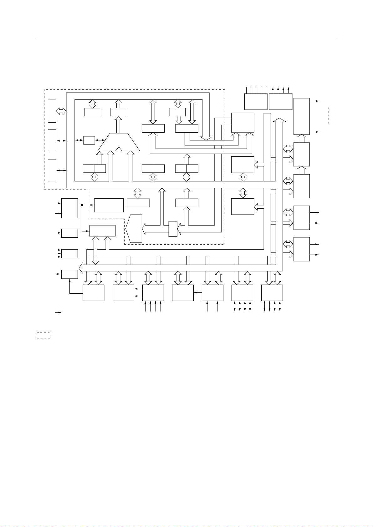
BLOCK DIAGRAM
SS3VSS2VSS1
COM4
COM3
COM2
C2C1V
COM1
OSC0
OSC1
RESET
TST1
TST2
TST3
V
SSL
BSRHALTMIEF
OSC
RST
TST
VR
TR2 TR0 TR1
(4)
C
BA HL XY
ALU
(4) (4)
TIMING
CONTROLLER
TBC
PCM PCL
DB7 to DB0
IR
DECODER
PCH
A7 to A0
ROMRSP
IR
PORT ADDRESS
DB7 to DB0
A8 to A11
(8)
(8)
ROM
3040B
RAM
160N
INTC
BIAS
COM
DRV
LCD
DRV
PORT ADDRESS
LCD
CNT
DSPR
MD0
MD1
SEG0
SEG35
MD0
MD0
MD1
MD1
BUP CAPR PORT2 EVENT PORT3 PORT6 PORT7
V
DD
is the CPU core (nX-4/20).
P2.0
P2.1
P2.2
P2.3
P3.0
P3.1
P6.0
P6.1
P6.2
P6.3
P7.0
P7.1
P7.2
P7.3
2/25
Page 3
¡ Semiconductor MSM64153A/64153AL
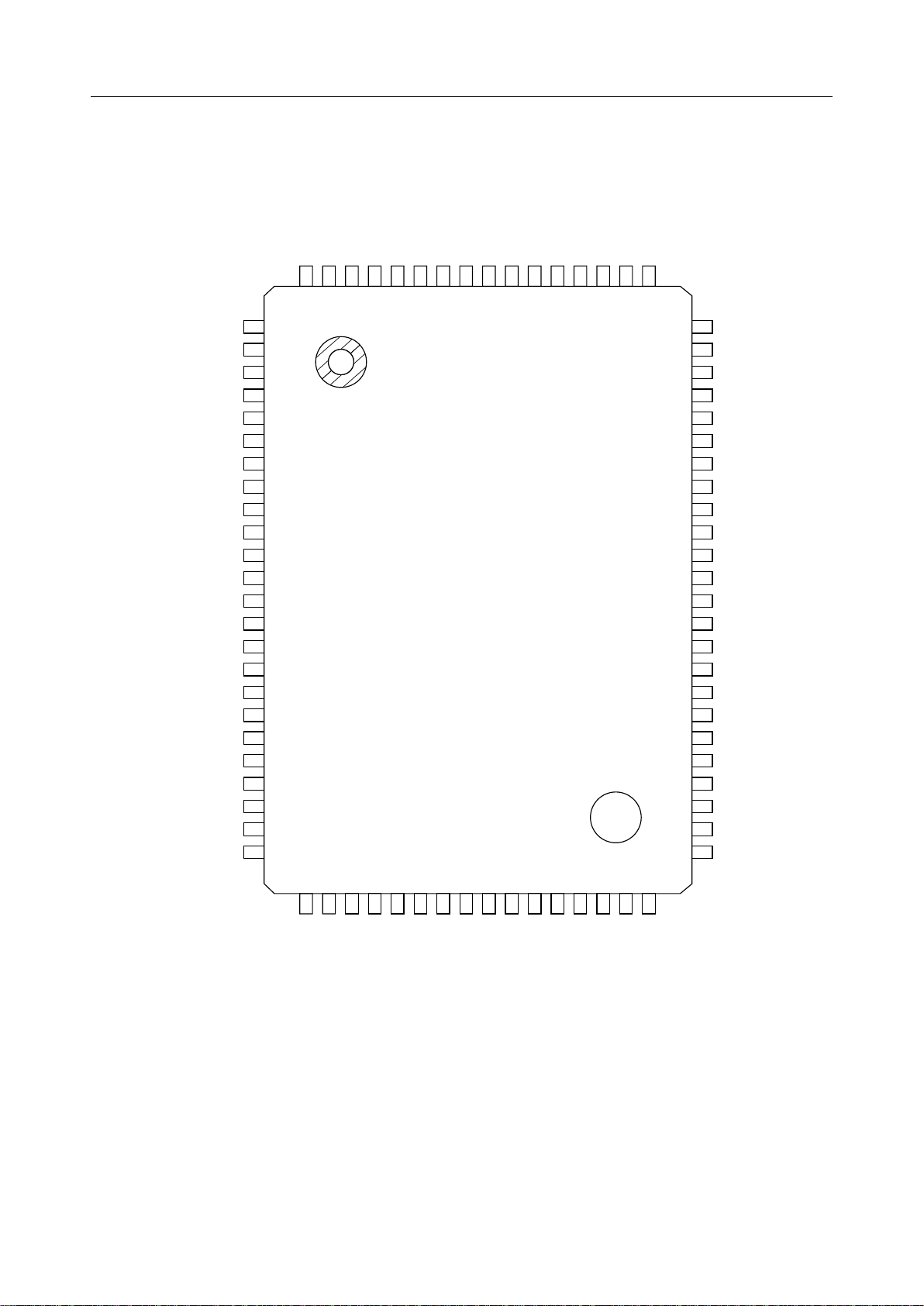
PIN CONFIGURATION (TOP VIEW)
SEG22
SEG21
SEG20
SEG19
SEG18
SEG17
SEG16
SEG15
SEG14
SEG13
SEG12
SEG11
SEG10
SEG8
79
SEG9
78
77
76
75
74
73
72
71
70
69
68
67
66
65
SEG7
80
SEG6
(NC)
SEG5
SEG4
SEG3
SEG2
SEG1
SEG0
(NC)
V
SSL
COM4
COM3
COM2
(NC)
COM1
C2
C1
V
SS3
V
SS2
V
SS1
TST3
(NC)
TST2
TST1
10
11
12
13
14
15
16
17
18
19
20
21
22
23
24
1
2
3
4
5
6
7
8
9
64
63
62
61
60
59
58
57
56
55
54
53
52
51
50
49
48
47
46
45
44
43
42
41
SEG23
(NC)
SEG24
SEG25
SEG26
SEG27
SEG28
SEG29
SEG30
SEG31
SEG32
(NC)
SEG33
SEG34
SEG35
MD0
MD0
MD1
MD1
V
DD
P7.0
(NC)
P7.1
P7.2
40
39
38
37
36
35
34
33
32
31
30
29
28
27
26
25
P7.3
P6.0
P6.1
P6.2
P6.3
P2.0
P2.1
P2.2
P2.3
P3.0
OSC0
P3.1
OSC1
(NC)
(NC)
RESET
80-Pin Plastic QFP
Note: Pins marked as (NC) are no-connection pins which are left open.
3/25
Page 4
¡ Semiconductor MSM64153A/64153AL
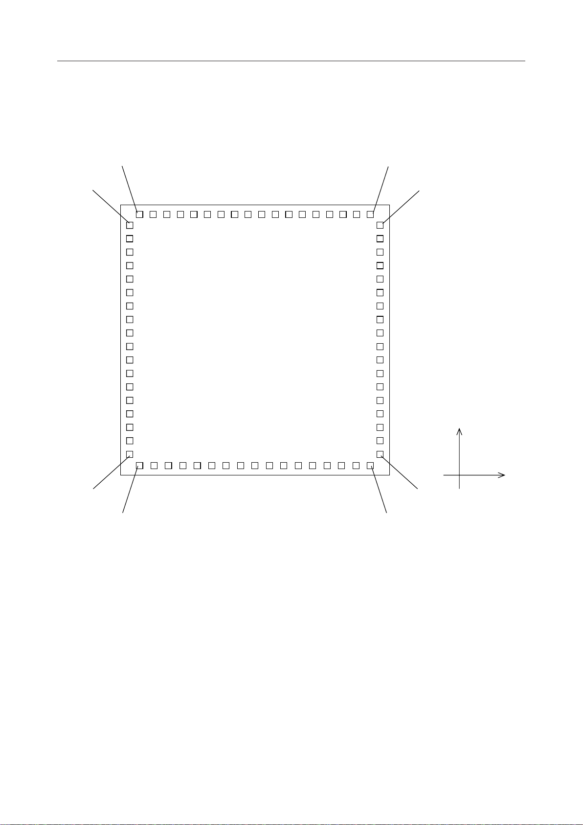
PAD CONFIGURATION
Pad Layout
54
53
36
35
Y
171
Chip Size : 4.08 mm ¥ 4.02 mm
Chip Thickness : 350 mm (typ.)
Coordinate Origin : Chip center
Pad Hole Size : 110 mm ¥ 110 mm
Pad Size : 120 mm ¥ 120 mm
Minimum Pad Pitch : 180 mm
Note: The chip substrate voltage is VDD.
X
1871
4/25
Page 5
¡ Semiconductor MSM64153A/64153AL
Pad Coordinates
Pad No. Y (µm)X (µm)Pad Name
1 –1809–1697SEG5
2 –1809SEG4
3 SEG3
4 SEG2
5 SEG1
6 SEG0
7V
SSL
8 COM4
9 COM3
10 COM2
11 COM1
12 C2
13 C1
14 V
15 V
16 V
SS3
SS2
SS1
17 TST3
18 –1712TST2
19 –1516TST1
20 OSC0
21
22
23
24
25
26
27
28
29
30
31
32
33
34
35
OSC1 –1123
P3.1 –927
P3.0 –730
P2.3 –536
P2.2 –338
P2.1 –141
P2.0 55
P6.3 251
P6.2 448
P6.1 644
P6.0 840
RESET 1036
P7.3 1233
P7.2 1429
P7.1 1625
36 1796P7.0
37 1585V
DD
38 1378MD1
39 1172MD1
40 962MD0
Pad No.
41 1809755MD0
–1482 547
–1270 339
–1058 131
–848 –77
–637
–424
–201
10
222
430
641
854
1065
1275
1486
1697
–1809
–1809
–1809
–1809
–1809
–1809
–1809
–1809
–1809
–1809
–1809
–1809
–1809
–1809
–1809
1889
1889
1889
–1319
1889
1889
1889
1889
1889
1889
1889
1889
1889
1889
1889
42 1809SEG35
43 SEG34
44
45
46
47
48
49
50
51
52
53
54
55
56
57
58
59
60
61
62
63
64
65
66
67
68
69
70
71
SEG33
SEG32
SEG31
SEG30
SEG29
SEG28
SEG27
SEG26
SEG25
SEG24
SEG23
SEG22
SEG21
SEG20
SEG19
SEG18
SEG17
SEG16
SEG15
SEG14
SEG13
SEG12
SEG11
SEG10
SEG9
SEG8
SEG7
SEG6
–284
–494
–701
–907
–1116
–1324
–1530
–1743
–1889
–1889
–1889
–1889
–1889
–1889
–1889
–1889
–1889
–1889
–1889
–1889
–1889
–1889
–1889
–1889
–1889
–1889
1889
1889
1889
1889
1809
1809
1809
1809
1809
Y (µm)X (µm)Pad Name
1809
1809
1809
1809
1809
1809
1809
1809
1809
1809
1809
1599
1409
1214
1019
829
639
449
260
70
–120
–310
–501
–693
–885
–1078
–1271
–1465
–1656
5/25
Page 6
¡ Semiconductor MSM64153A/64153AL
PIN DESCRIPTIONS
Basic Functions
Function
Power
Supply
Oscillation
Test
RESET
Pin
45
20
19
18
17
16
10
25
26
24
23
21
39 32 I
Pad
37
16
15
14
13
12
7
20
21
19
18
17
Symbol
V
DD
V
SS1
V
SS2
V
SS3
C1
C2
V
SSL
OSCO
OSC1
TST1
TST2
TST3
RESET
DescriptionType
—
Digital supply voltage (0 V)
—
Digital negative power supply (1.5 V spec.)
Bias output for LCD driver (3.0 V spec.)
—
Digital negative power supply (3.0 V spec.)
Bias output for LCD driver (1.5 V spec.)
Bias output for LCD driver (–4.5 V)
—
—
For connection to capacitors that generate bias for the
LCD driver
—
—
Negative power supply voltage pin for internal logic
(An internally generated constant voltage is present at this pin.)
I
Clock oscillation pins:
Either a crystal (32.768 kHz) and a capacitor (10 to 30 pF)
are connected to these pins or a resistor (1 MW) is.
O
I
Input pins for test
I
I
System reset input pin :
Setting this pin to "H" level puts this device into a reset state.
Then, setting this pin to "L" level starts executing an
instruction from address 0000H.
This pin is internally connected to V
SS1
or V
through a
SS2
pull-down resistor.
6/25
Page 7
¡ Semiconductor MSM64153A/64153AL
Basic Functions (continued)
PadPin DescriptionTypeFunction
Ports 4-bit input port (port 2) :
31
30
29 24
28
27
37
36
35 28
42
41
40 33
2733
26
25
23
22
3138
30
29
3644
35
34
Symbol
P2.0
P2.1
P2.2
P2.3
P3.0
P3.1
P6.0
P6.1
P6.2
P6.3
P7.0
P7.1
P7.2
P7.3
I
Select between pull-down resistor input and high impedance
input for each bit with the port 2 control register (P2CON).
When configured for secondary functions, an external
interrupt and capture circuit trigger input are allocated.
If P2.0 to P2.3 are set to "H" level, the device enters system
reset mode.
I 2-bit input port (port 3) :
Select between pull-down resistor input and high impedance
input with the port 3 control register (P3CON).
When configured for a secondary function, an external
interrupt is allocated to P3.0 and an event counter is
allocated to P3.1.
4-bit input-output port (port 6) :
I/O
Select between input and output, between pull-down resistor
input and high impedance input, and between open-drain
output and CMOS output with the port 6 control register
(P6CON). When configured for a secondary function, an
external interrupt is allocated.
4-bit input-output port (port 7) :
I/O
Select between input and output, between pull-down
resistor input and high impedance input, and between
open-drain output and CMOS output with the port 7 control
register (P7CON). When configured for a secondary
function, an external interrupt is allocated.
Melody
Drivers
LCD
Drivers
13
12
11 8
1115
10
9
MD0
MD0
MD1
MD1
COM1
COM2
COM3
COM4
O Output pin of melody driver 04048
O Inverted output pin of MD0 output4149
O Output pin of melody driver 13846
O Inverted output pin of MD1 output3947
O
LCD common signal output pins
O
O
O
7/25
Page 8
¡ Semiconductor MSM64153A/64153AL
Basic Functions (continued)
LCD
Drivers
PadPin DescriptionTypeFunction
68
Symbol
SEG0
SEG1
SEG2
SEG3
SEG4
SEG5
SEG6
SEG7
SEG8
SEG9
SEG10
SEG11
SEG12
SEG13
SEG14
SEG15
SEG16
O
LCD segment signal output pins
O57
O46
O35
O24
O13
O711
O7080
O6979
O6878
O6777
O6676
O6575
O6474
O6373
O6272
O6171
SEG17
SEG18
SEG19
SEG20
SEG21
SEG22
SEG23
SEG24
SEG25
SEG26
SEG27
SEG28
SEG29
SEG30
SEG31
SEG32
SEG33
SEG34
O6070
O5969
O5868
O5767
O5666
O5565
O5464
O5362
O5261
O5160
O5059
O4958
O4857
O4756
O4655
O4554
O4452
O4351
SEG35
O4250
8/25
Page 9

¡ Semiconductor MSM64153A/64153AL
Secondary Functions
External
Interrupts
PadPin DescriptionTypeFunction
2733
2631
2530
2429
2328
3138
3037
2936
2835
3644
3542
3441
Symbol
P2.0
P2.1
P2.2
P2.3
P3.0
P6.0
P6.1
P6.2
P6.3
P7.0
P7.1
P7.2
I
P2.0 to P2.3 secondary functions :
These are level-triggered external interrupt input pins.
Select interrupt enable/disable for each bit with the
P2 interrupt enable register (P2IE).
If P2.0 to P2.3 pins are set to "H" level for a minimum
of 2 seconds, the device enters system reset mode.
P2.0, P2.1 secondary functions :
trigger input pins for capture circuit.
I
P3.0 secondary function :
This is an input pin for external interrupt. This pin can
receive an interrupt at a rising edge, a falling edge, or at
both rising and falling edges.
I
P6.0 to P6.3 secondary functions :
These are level-triggered external interrupt input pins.
I
P7.0 to P7.3 secondary functions :
These are level-triggered external interrupt input pins.
Counter
Input
3340
2227Event
P7.3
P3.1
I
P3.1 secondary function :
Input port for event counter
9/25
Page 10

¡ Semiconductor MSM64153A/64153AL
Handling When Specific Pins Are Not Used
Symbol
TST1 to TST3
P2.0 to P2.3
P3.0, P3.1
P6.0 to P6.3
P7.0 to P7.3
MD0, MD0
MD1, MD1
COM1 to COM4
SEG0 to SEG35
Recommended Pin Connection
Open
"L" level or open
"L" level or open
In input mode : "L" level or open (Initial setting: input mode)
In output mode : Open
In input mode : "L" level or open (Initial setting: input mode)
In output mode : Open
Open
Open
Open
10/25
Page 11

¡ Semiconductor MSM64153A/64153AL
ABSOLUTE MAXIMUM RATINGS
1.5 V Spec. (MSM64153A)
= 0 V)
(V
DD
Parameter Symbol Condition Rating Unit
Power Supply Voltage 1
Power Supply Voltage 2
Power Supply Voltage 3
Power Supply Voltage 4
Input Voltage 1
Input Voltage 2
Output Voltage 1
Output Voltage 2
Output Voltage 3
Output Voltage 4
Storage Temperature
V
V
V
V
V
V
V
V
V
V
T
SS1
SS2
SS3
SSL
IN1
IN2
OUT1
OUT2
OUT3
OUT4
STG
Ta = 25°C –2.0 to +0.3 V
Ta = 25°C –4.0 to +0.3 V
Ta = 25°C –5.5 to +0.3 V
Ta = 25°C –2.0 to +0.3 V
V
input, Ta = 25°C V
SS1
V
input,Ta = 25°C V
SSL
V
output,Ta = 25°C V
SS1
V
output,Ta = 25°C V
SS2
V
output,Ta = 25°C V
SS3
V
output,Ta = 25°C V
SSL
– 0.3 to +0.3 V
SS1
– 0.3 to +0.3 V
SSL
– 0.3 to +0.3 V
SS1
– 0.3 to +0.3 V
SS2
– 0.3 to +0.3 V
SS3
– 0.3 to +0.3 V
SSL
— –55 to +150 °C
RECOMMENDED OPERATING CONDITIONS
1.5 V Spec. (MSM64153A)
Parameter Symbol Condition Range Unit
Operating Temperature
Operating Voltage
Crystal Oscillation Frequency
External RC Oscillator Resistance
T
op
V
SS1
f
XT
R
OS
— –40 to +70 °C
BUPF = "0" –1.7 to –1.25
BUPF = "1" –1.7 to –1.15
— 30 to 35 kHz
— 1M ±10% W
(V
DD
= 0 V)
V
11/25
Page 12

¡ Semiconductor MSM64153A/64153AL
ELECTRICAL CHARACTERISTICS
1.5 V Spec. (MSM64153A)
DC Characteristics
(V
= 0 V, V
DD
Parameter Symbol Condition Min. Typ. Max. Unit
Ca, Cb, C
= 0.1 mF
12
Ta = –40 to +60°C
BUPF = "0"
C
a
, Cb, C
= 0.1 mF
12
Ta = –40 to +70°C
BUPF = "0"
V
SS2
Voltage
V
SS2
C
a
, Cb, C
= 0.1 mF
12
Ta = –40 to +60°C
BUPF = "1"
C
a
, Cb, C
= 0.2 mF
12
Ta = –40 to +70°C
BUPF = "1"
C
a
, Cb, C
= 0.1 mF
12
Ta = –40 to +60°C
BUPF = "0"
C
a
, Cb, C
= 0.1 mF
12
Ta = –40 to +70°C
BUPF = "0"
V
Voltage
SS3
V
SS3
C
a
, Cb, C
= 0.1 mF
12
Ta = –40 to +60°C
BUPF = "1"
C
a
, Cb, C
= 0.2 mF
12
Ta = –40 to +70°C
BUPF = "1"
BUPF = "0"
Voltage
V
SSL
Crystal Oscillation
Start Voltage
V
SSL
BUPF = "1"
V
Oscillation start time:
STA
within 5 seconds after reset
Crystal Oscillation
V
Hold Voltage
HOLD
External Crystal
C
Oscillator Capacitance
G
Internal Crystal
C
Oscillator Capacitance
D
RC Oscillation
Frequency
f
CR
R
OS
= 1 MW
= –1.5 V, Ta = –40 to +70°C unless otherwise specified.)
SS1
+100%
–20%
–3.2
–3.0
–2.8
+100%
–20%
+100%
–20%
–3.2
–3.2
–3.0
–3.0
–2.7
V
–2.5
+100%
–20%
–3.2
–3.0
–2.3
+100%
–20%
–4.7
–4.5
–4.2
+100%
–20%
+100%
–20%
–4.7
–4.7
–4.5
–4.5
–4.0
V
–3.9
+100%
–20%
–4.7
–1.5
–4.5
–1.3
–3.7
–0.6
V
–0.6
–1.3
–1.9
—
—
—
—
—
10
10
—
—
—
15
–1.45
–1.15
30
20
V
V
pF
pF
15 40 75 kHz
Measuring
Circuit
1
1'
1
1'
12/25
Page 13

¡ Semiconductor MSM64153A/64153AL
DC Characteristics (continued)
• 32.768 kHz crystal oscillation
(V
= 0 V, V
DD
= –1.5 V, Ta = –40 to +70°C unless otherwise specified.)
SS1
Measuring
Parameter Symbol Condition Min. Typ. Max. Unit
Supply Current 1
Supply Current 1
Supply Current 2
Supply Current 2
I
DD1
I
DD1
I
DD2
I
DD2
CPU is in HALT state
BUPF = "0"
CPU is in HALT state
BUPF = "1"
CPU is in operation state
BUPF = "0"
CPU is in operation state
BUPF = "1"
Ta = –40 to +40°C
Ta = +40 to +70°C
Ta = –40 to +40°C
Ta = +40 to +70°C
Ta = –40 to +40°C
Ta = +40 to +70°C
Ta = –40 to +40°C
Ta = +40 to +70°C
—
—
—
—
—
—
—
—
2.0
6.0
2.0
40
3.0
3.0
50
6.0
15
6.01050
10
25
10
60
mA
mA
mA
mA
mA
mA
mA
mA
Circuit
1
• RC oscillation
(V
= 0 V, V
DD
= –1.5 V, R
SS1
= 1 MW, Ta = –40 to +70°C unless otherwise specified.)
OS
Parameter Symbol Condition Min. Typ. Max. Unit
Supply Current 1
Supply Current 1
Supply Current 2
Supply Current 2
I
I
I
I
DD1
DD1
DD2
DD2
CPU is in HALT state
BUPF = "0"
CPU is in HALT state
BUPF = "1"
CPU is in operation state
BUPF = "0"
CPU is in operation state
BUPF = "1"
Ta = –40 to +40°C
Ta = +40 to +70°C
Ta = –40 to +40°C
Ta = +40 to +70°C
Ta = –40 to +40°C
Ta = +40 to +70°C
Ta = –40 to +40°C
Ta = +40 to +70°C
—
—
—
—
—
—
—
—
3.0
10
3.0
45
6.0
6.0
50
7.0
20
7.01550
15
30
15
70
Measuring
mA
mA
mA
mA
mA
mA
mA
mA
Circuit
1'
13/25
Page 14

¡ Semiconductor MSM64153A/64153AL
DC Characteristics (continued)
(V
= 0 V, V
DD
Parameter
(Pin Name)
Output Current 1
(MD0, MD0)
(MD1, MD1)
= V
SS1
= –1.5 V, V
SSL
= –3.0 V, V
SS2
= –4.5 V, Ta = –40 to +70°C unless otherwise specified.)
SS3
Symbol Condition Min. Typ. Max. Unit
I
I
OH1
OL1
V
V
OH1
OL1
= –0.5 V
= V
SS1
+ 0.5 V
–2.0
–0.6
–0.1
0.1 0.6 2.0 mA
Measuring
Circuit
mA
Output Current 2
(SEG0 to SEG35)
(COM1 to COM4)
Output Current 3
(P6.0 to P6.3)
(P7.0 to P7.3)
Output Leakage
Current
(P6.0 to P6.3)
(P7.0 to P7.3)
Input Current 1
(P2.0 to P2.3)
(P3.0, P3.1)
(P6.0 to P6.3)
(P7.0 to P7.3)
I
OH2
I
OMH2
I
OMH2S
I
OML2
I
OML2S
I
OL2
I
OH3
I
OL3
I
OOH
I
OOL
I
IH1
I
IH1Z
I
IL1
V
OH2
V
OMH2
V
OMH2S
V
OML2
V
OML2S
V
OL2
V
OH3
V
OL3
V
OH
V
OL
V
IH1
V
IH1
V
IL1
= –0.2 V
= V
= V
= V
= V
= V
SS3
= –0.5 V
= V
SS1
= V
DD
= V
SS1
= V
DD
= V
DD
= V
SS1
(V
DD
SS1
SS1
SS2
SS2
+ 0.2 V
+ 0.2 V
– 0.2 V
+ 0.2 V
– 0.2 V
(V
(V
(V
(V
(V
SS1
SS1
SS2
SS2
SS3
+ 0.5 V
(When pulled down)
(In a high-impedance state)
level)
level)
level)
level)
level)
level)
—
—
4.0
—
4.0
–4.0
——
— –4.0
—
—
mA
mA
mA
mA
— — –4.0 mA
4.0 — — mA
–5.0 –2.1 –0.3 mA
0.1 0.7 2.0 mA
— — 0.3 mA
–0.3 — — mA
1.0
100
mA
0 — 1.0 mA
–1.0
—0
mA
2
3
Input Current 2
(TST1, TST2, TST3)
Input Current 3
(RESET)
Input Voltage 1
(P2.0 to P2.3)
(P3.0, P3.1)
(P6.0 to P6.3)
(TST1, TST2,
TST3)
(RESET)
I
IH2
I
I
IH3
I
V
IL2
IL3
IH1
V
= V
IH2
DD
V
= V
IL2
SS1
V
= V
IH3
DD
V
= V
IL3
SS1
—
0.3
0.75 1.5
–1.020—
mA
0
mA
15 40 100 mA
–1.0 — 0 mA
–0.3 — 0 V
4
V
IL1
—
–1.5 — –1.2 V
14/25
Page 15

¡ Semiconductor MSM64153A/64153AL
Measuring circuit 1
V
SSL
C
L
Measuring circuit 1'
OSC1
Crystal
32.768 kHz
V
DD
C
G
OSC0
MSM64153A
C1
C
12
C2
V
DD
AV V V
V
SS1VSS2
C
V
SS3
Ca, Cb, C
C
a
b
C
C
12
L
G
: 0.1 to 0.2 mF
: 0.1 mF
: 15 pF
OSC1
R
OS
OSC0
MSM64153A
C1
C
12
V
SSL
V
C
L
DD
V
SS1VSS2
C
V
SS3
a
C
b
V VAV
C2
Ca, Cb, C
C
L
R
OS
12
: 0.1 to 0.2 mF
: 0.1 mF
: 1 MW
15/25
Page 16

¡ Semiconductor MSM64153A/64153AL
Measuring circuit 2
(*2)
V
IH
(*1)
V
IL
Measuring circuit 3
(*3)
A
INPUT
V
DD
MSM64153A
V
SS1VSS2VSS3VSSL
A
OUTPUT
INPUT
V
DD
MSM64153A
V
SS1VSS2VSS3VSSL
OUTPUT
16/25
Page 17

¡ Semiconductor MSM64153A/64153AL
Measuring circuit 4
V
IH
(*3)
V
IL
INPUT
V
DD
MSM64153A
V
SS1VSS2
V
SS3VSSL
*1 Input logic circuit to determine the specified measuring conditions.
*2 Measured at the specified output pins.
*3 Measured at the specified input pins.
Waveform
Monitoring
OUTPUT
17/25
Page 18

¡ Semiconductor MSM64153A/64153AL
ABSOLUTE MAXIMUM RATINGS
3.0 V Spec. (MSM64153AL)
(V
= 0 V)
DD
Parameter Symbol Condition Rating Unit
Power Supply Voltage 1
Power Supply Voltage 2
Power Supply Voltage 3
Power Supply Voltage 4
Input Voltage 1
Input Voltage 2
Output Voltage 1
Output Voltage 2
Output Voltage 3
Storage Temperature
V
V
V
V
V
V
V
V
V
T
SS1
SS2
SS3
SSL
IN1
IN2
OUT1
OUT2
OUT3
STG
Ta = 25°C –2.0 to +0.3 V
Ta = 25°C –4.0 to +0.3 V
Ta = 25°C –5.5 to +0.3 V
Ta = 25°C –4.0 to +0.3 V
V
input, Ta = 25°C V
SS2
V
input,Ta = 25°C V
SSL
V
output,Ta = 25°C V
SS2
V
output,Ta = 25°C V
SS3
V
output,Ta = 25°C V
SSL
– 0.3 to +0.3 V
SS2
– 0.3 to +0.3 V
SSL
– 0.3 to +0.3 V
SS2
– 0.3 to +0.3 V
SS3
– 0.3 to +0.3 V
SSL
— –55 to +150 °C
RECOMMENDED OPERATING CONDITIONS
3.0 V Spec. (MSM64153AL)
Parameter Symbol Condition Range Unit
Operating Temperature
Operating Voltage
Crystal Oscillation Frequency
External RC Oscillator Resistance
T
op
V
SS2
f
XT
R
OS
— –40 to +70 °C
BUPF = "0" –3.5 to –2.5
BUPF = "1" –3.5 to –2.0
— 30 to 66 kHz
— 1 M ±10% W
(V
DD
= 0 V)
V
18/25
Page 19

¡ Semiconductor MSM64153A/64153AL
ELECTRICAL CHARACTERISTICS
3.0 V Spec. (MSM64153AL)
DC Characteristics
(V
= 0 V, V
DD
Parameter Symbol Condition Min. Typ. Max. Unit
= –3.0 V, Ta = –40 to +70°C unless otherwise specified.)
SS2
Measuring
Circuit
V
Voltage
SS1
Voltage
V
SS3
Voltage
V
SSL
Crystal Oscillation
Start Voltage
Crystal Oscillation
Hold Voltage
External Crystal
Oscillator Capacitance
Internal Crystal
Oscillator Capacitance
RC Oscillation
Frequency
V
V
V
V
V
HOLD
C
C
f
SS1
SS3
Ca, Cb, C
, Cb, C
C
a
= 0.1 mF
12
= 0.1 mF
12
BUPF = "0"
SSL
BUPF = "1"
Oscillation start time:
STA
within 5 seconds after reset
G
D
= 1 MW
R
CR
OS
+100%
–20%
+100%
–20%
—
—
—
–1.7 –1.5 –1.3
V
–4.7 –4.5 –4.2 V
–1.5 –1.3 –0.6
V
–1.9 –1.3 –0.6
—
V— –2.5
— — –2.0 V
10—30pF
10 15 20 pF
15 40 75 kHz
1
1'
1
1'
19/25
Page 20

¡ Semiconductor MSM64153A/64153AL
DC Characteristics (continued)
• 32.768 kHz crystal oscillation
(V
= 0 V, V
DD
= –3.0 V, Ta = –40 to +70°C unless otherwise specified.)
SS2
Measuring
Parameter Symbol Condition Min. Typ. Max. Unit
Supply Current 1
Supply Current 1
Supply Current 2
Supply Current 2
I
I
I
I
DD1
DD1
DD2
DD2
CPU is in HALT state
BUPF = "0"
CPU is in HALT state
BUPF = "1"
CPU is in operation state
BUPF = "0"
CPU is in operation state
BUPF = "1"
Ta = –40 to +40°C
Ta = +40 to +70°C
Ta = –40 to +40°C
Ta = +40 to +70°C
Ta = –40 to +40°C
Ta = +40 to +70°C
Ta = –40 to +40°C
Ta = +40 to +70°C
—
—
—
—
—
—
—
—
0.9
0.9
1.5
1.5
3.0
3.0
5.0
5.0
4.5
30
6.0
40
10
40
15
50
mA
mA
mA
mA
mA
mA
mA
mA
Circuit
1
• RC oscillation
(V
= 0 V, V
DD
= –3.0 V, R
SS2
= 1 MW, Ta = –40 to +70°C unless otherwise specified.)
OS
Parameter Symbol Condition Min. Typ. Max. Unit
Supply Current 1
Supply Current 1
Supply Current 2
Supply Current 2
I
DD1
I
DD1
I
DD2
I
DD2
CPU is in HALT state
BUPF = "0"
CPU is in HALT state
BUPF = "1"
CPU is in operation state
BUPF = "0"
CPU is in operation state
BUPF = "1"
Ta = –40 to +40°C
Ta = +40 to +70°C
Ta = –40 to +40°C
Ta = +40 to +70°C
Ta = –40 to +40°C
Ta = +40 to +70°C
Ta = –40 to +40°C
Ta = +40 to +70°C
—
—
—
—
—
—
—
—
1.5
6.0
1.5
40
3.0
3.0
50
4.0
12
4.01050
8.0
25
8.0
60
Measuring
mA
mA
mA
mA
mA
mA
mA
mA
Circuit
1'
20/25
Page 21

¡ Semiconductor MSM64153A/64153AL
DC Characteristics (continued)
(V
= 0 V, V
DD
Parameter
(Pin Name)
Output Current 1
(MD0, MD0)
(MD1, MD1)
= V
SS1
= –1.5 V, V
SSL
= –3.0 V, V
SS2
= –4.5 V, Ta = –40 to +70°C unless otherwise specified.)
SS3
Symbol Condition Min. Typ. Max. Unit
I
OH1
I
OL1
V
V
OH1
OL1
= –0.5 V
= V
SS2
+ 0.5 V
–6.0
–1.8
–0.7
0.7 1.8 6.0 mA
Measuring
Circuit
mA
Output Current 2
(SEG0 to SEG35)
(COM1 to COM4)
Output Current 3
(P6.0 to P6.3)
(P7.0 to P7.3)
Output Leakage
Current
(P6.0 to P6.3)
(P7.0 to P7.3)
Input Current 1
(P2.0 to P2.3)
(P3.0, P3.1)
(P6.0 to P6.3)
(P7.0 to P7.3)
I
OH2
I
OMH2
I
OMH2S
I
OML2
I
OML2S
I
OL2
I
OH3
I
OL3
I
OOH
I
OOL
I
IH1
I
IH1Z
I
IL1
V
OH2
V
OMH2
V
OMH2S
V
OML2
V
OML2S
V
OL2
V
OH3
V
OL3
V
OH
V
OL
V
IH1
V
IH1
V
IL1
= –0.2 V
= V
= V
= V
= V
= V
SS3
= –0.5 V
= V
SS2
= V
DD
= V
SS2
= V
DD
= V
DD
= V
SS2
(V
DD
SS1
SS1
SS2
SS2
+ 0.2 V
+ 0.2 V
– 0.2 V
+ 0.2 V
– 0.2 V
(V
(V
(V
(V
(V
SS1
SS1
SS2
SS2
SS3
+ 0.5 V
(When pulled down)
(In a high-impedance state)
level)
level)
level)
level)
level)
level)
—
—
4.0
—
4.0
–4.0
——
— –4.0
—
—
mA
mA
mA
mA
— — –4.0 mA
4.0 — — mA
–18 –6.0 –2.0
mA
0.7 1.6 6.0 mA
— — 0.3 mA
–0.3 — — mA
50
100—300
mA
0 — 1.0 mA
–1.0
—0
mA
2
3
Input Current 2
(TST1, TST2, TST3)
Input Current 3
(RESET)
Input Voltage 3
(P2.0 to P2.3)
(P3.0, P3.1)
(P6.0 to P6.3)
(TST1, TST2,
TST3)
(RESET)
I
IH2
I
IL2
I
IH3
I
IL3
V
IH1
V
= V
IH2
DD
V
= V
IL2
SS2
V
= V
IH3
DD
V
= V
IL3
SS2
—
0.75
–1.0
1.5 3.0
mA
0
mA
40 80 200 mA
–1.0 — 0 mA
–0.6 — 0 V
4
V
IL1
—
–3.0 — –2.4 V
21/25
Page 22

¡ Semiconductor MSM64153A/64153AL
Measuring circuit 1
V
C
L
Measuring circuit 1'
SSL
OSC1
Crystal
32.768 kHz
V
DD
C
G
OSC0
MSM64153AL
C1
C
12
C2
V
DD
AV V V
V
SS2VSS1
C
V
SS3
Ca, Cb, C12, C
C
C
a
b
G
L
: 0.1 mF
: 15 pF
OSC1
R
OS
OSC0
MSM64153AL
C1
C
12
V
SSL
V
C
L
DD
V
SS2
V
SS1
C
a
V
SS3
C
b
V VAV
C2
Ca, Cb, C12, C
R
OS
L
: 0.1 mF
:1 MW
22/25
Page 23

¡ Semiconductor MSM64153A/64153AL
Measuring circuit 2
(*2)
V
IH
(*1)
V
IL
Measuring circuit 3
(*3)
INPUT
V
DD
MSM64153AL
V
SS1VSS2VSS3
V
A
OUTPUT
SSL
A
MSM64153AL
INPUT
V
DD
V
SS1VSS2VSS3VSSL
OUTPUT
23/25
Page 24

¡ Semiconductor MSM64153A/64153AL
Measuring circuit 4
V
IH
(*3)
V
IL
INPUT
V
DD
MSM64153AL
V
SS1
V
SS2VSS3VSSL
*1 Input logic circuit to determine the specified measuring conditions.
*2 Measured at the specified output pins.
*3 Measured at the specified input pins.
Waveform
Monitoring
OUTPUT
24/25
Page 25

¡ Semiconductor MSM64153A/64153AL
PACKAGE DIMENSIONS
(Unit : mm)
QFP80-P-1420-0.80-BK
Mirror finish
Package material
Lead frame material
Pin treatment
Solder plate thickness
Package weight (g)
Epoxy resin
42 alloy
Solder plating
5 mm or more
1.27 TYP.
Notes for Mounting the Surface Mount Type Package
The SOP, QFP, TSOP, SOJ, QFJ (PLCC), SHP and BGA are surface mount type packages, which
are very susceptible to heat in reflow mounting and humidity absorbed in storage.
Therefore, before you perform reflow mounting, contact Oki’s responsible sales person for the
product name, package name, pin number, package code and desired mounting conditions
(reflow method, temperature and times).
25/25
 Loading...