

Page 1

E2E0015-38-93
¡ Semiconductor
This version: Sep. 1998
Previous version: Mar. 1996
MSM6411A¡ Semiconductor
MSM6411A
High speed and Simple 4-Bit Microcontroller
GENERAL DESCRIPTION
The MSM6411A, implemented in complementary metal-oxide semiconductor technology, is a
low-power CMOS 4-bit microcontroller developed for smaller-scale control systems.
FEATURES
• ROM : 1024 words ¥ 8 bits
• RAM : 32 words ¥ 4 bits
• I/O port
Input-output port : 2 ports ¥ 4 bits
Input port : 1 port ¥ 3 bits
• 8-bit serial shift register
• 2 interrupt sources (1 external, 1 internal)
• 63 instructions
• Power-down features
• Minimum instruction execution time : 952 ns @ 4.2 MHz clock
• Single 5 V power supply
• Package:
16-pin plastic DIP (DIP16-P-300-2.54) : (Product name : MSM6411A-¥¥RS)
¥¥ indicates a code number.
1/11
Page 2
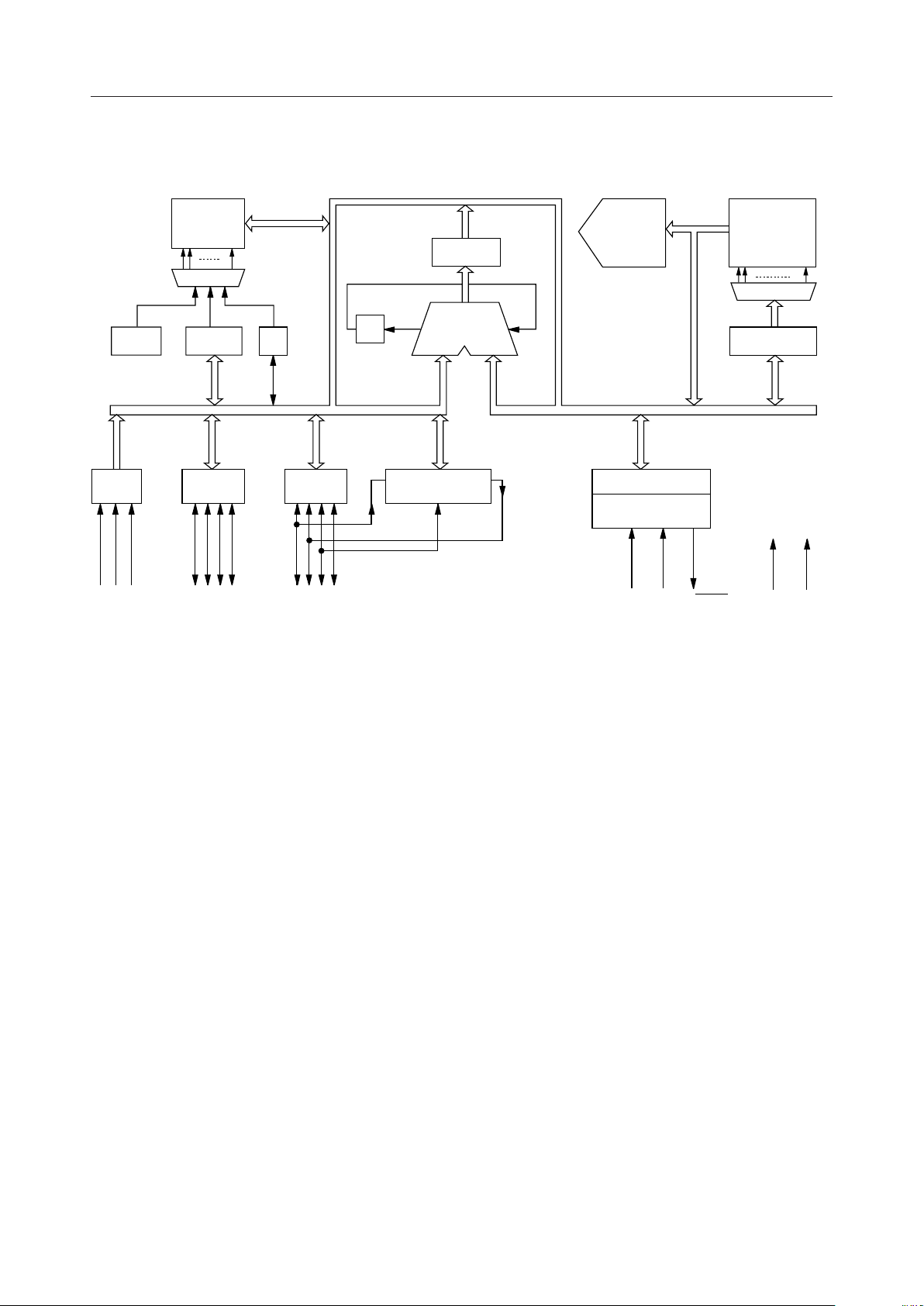
BLOCK DIAGRAM
MSM6411A¡ Semiconductor
RAM
32 ¥ 4 bits
DEC
2 0
P2
2 1 0
SP
L
3 0
P1
3 2 1 0
INT SISO
H
P0
3 2 1 0
SCK
C
I SR O
7 f 0
ACC
3 0
ALU
INST.
DEC.
RESET
INT.C
T.G
OSC
ROM
1024 ¥ 8 bits
DEC
PC
9 0
1
VDDGND
OSC
0
2/11
Page 3
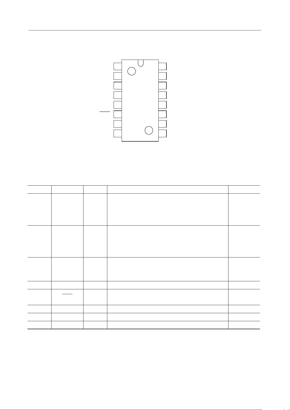
PIN CONFIGURATION (TOP VIEW)
MSM6411A¡ Semiconductor
P1.2
P1.3
P2.0/INT
P2.1
P2.2
OSC
OSC
GND
1
2
3
4
5
6
1
7
0
8
16
15
14
13
12
11
10
9
V
DD
P1.1
P1.0
P0.3/SI
P0.2/SO
P0.1/SCK
P0.0
RESET
16-Pin Plastic DIP
PIN DESCRIPTIONS
Pin
10
11
12
13
14
15
1
2
3
4
5
7
6
9
16
8I —
Symbol Type Description During reset
P0.0
P0.1/SCK
I/O
P0.2/SO
4-bit input-output port. P0.1 to P0.3 are used as both
input-output ports and shift register pins.
"1"
P0.3/SI
P1.0
P1.1
I/O 4-bit input-output port. "1"
P1.2
P1.3
P2.0/INT
P2.1
I
and INT input pin (falling edge trigger input).
3-bit input port with latch. P2.0 is used as both input port
Latch is reset.
("0")
P2.2
OSC
0
OSC
1
RESET I Input pin for system reset.
V
DD
GND
I System clock input pin. Clocked in
O
the oscillator circuit.
System clock output pin. This pin and OSC
pin make up
0
—
—
I Power supply voltage pin.
—
Ground pin.
3/11
Page 4
INSTRUCTION LIST
Mnemonic Byte DescriptionCode Cycle
LAI n 1 A¨n90-9F 1
LLI n 1 L¨n80-8F 1
LHLI nn 2 HL¨nn15nn 2
LAL 1 A¨L21 1
LLA 1 L¨A2D 1
LAM 1 A¨M38 1
LMA 1 M¨A2F 1
LAMD mm 2 A¨Md10mm 2
LMAD mm 2 Md¨A11mm 2
LMSR 2 M(w)¨SR3E5A 2
Load, Push, Pop, ExchangeArithmetic Increment and Decrement
LSRM 2 SR¨M(w)3E52 2
PUSH 1 ST¨C, A, H, L, SP¨SP – 11C 3
POP 1 C, A, H, L¨ST, SP¨SP + 11D 3
X1A¨M28 1
INL 1 L¨L + 1, SKIP IF L = "0"31 1
INH 1 H¨H + 1, SKIP IF H = "0"32 1
INM 1 M¨M + 1, SKIP IF M = "0"33 1
INMD mm 2 Md¨Md – 1, SKIP IF Md = "0"12mm 2
DCL 1 L¨L – 1, SKIP IF L = "F"35 1
DCH 1 H¨H – 136 1
DCM 1 M¨M – 1, SKIP IF M = "F"37 1
ADS 1 A¨A + M, SKIP IF Cy = "1"02 1
ADC 1 C, A¨C + A + M03 1
AIS n 2 A¨A + n, SKIP IF Cy = "1"3E4n 2
DAS 1 A¨A + 100A 1
AND 1 A¨A M0D 1
EOR 1 A¨A M04 1
CMA 1 A¨A0B 1
CAM 1 SKIP IF A = M16 1
SC 1 C¨"1"07 1
RC 1 C¨"0"08 1
TC 1 SKIP IF C = "1"09 1
RAL 10E 1
MSM6411A¡ Semiconductor
A
C¨3¨2¨1¨0¨
4/11
Page 5

INSTRUCTION LIST (continued)
Mnemonic Byte DescriptionCode Cycle
TAB n2 1 SKIP IF [A bit n2] = "1"54-57 1
TMB n2 1 SKIP IF [M bit n2] = "1"58-5B 1
RMB n2 1 [M bit n2]¨"0"68-6B 1
SMB n2 1 [M bit n2]¨"1"78-7B 1
TPBD p•n2 2 SKIP IF [Pp bit n2] = "1"3D p0 to 3 2
RPBD p•n2 2 [Pp bit n2]¨"0"3D p4 to 7 2
SPBD p•n2 2 [Pp bit n2]¨"1"3D p8 to B 2
MEI 2 MEIF¨"1"3E60 2
MDI 2 MEIF¨"0"3E61 2
EICT 2 EICTF¨"1"3DCB 2
EIEX 2 EIEXF¨"1"3DC8 2
DICT 2 EICTF¨"0"3DC7 2
DIEX 23DC4 2
TICT 2 SKIP IF EICTF = "1"3DC3 2
Interrupt
TIEX 2 SKIP IF EIEXF = "1"3DC0 2
TQEX 2 SKIP IF IRQEX = "1"3D20 2
TQSR 2 SKIP IF IRQSR = "1"3DD3 2
RQEX 2 IRQEX¨"0"3D24 2
RQSR 2 IRQSR¨"0"3DD7 2
ESR 2 SRF¨"1"3DBA 2
DSR 2 SRF¨"0"3DB6 2
Shift
register
TSR 2 SKIP IF SRF = "1"3DB2 2
JCP a
6
JP a
10
Branch Bit manipulation
CAL a
10
RT 1 PC¨ST, SP¨SP + 1IE 4
IPD p 2 A¨Pp3DpD 2
Input/
output
OPD p 2 Pp¨A3DpC 2
STOP 2 STOP CLOCK3DB9 2
CPU
NOP 1 NO OPERATION00 1
control
C0 to FF 1
40 to 43
00 to FF
A0 to A3
00 to FF
MSM6411A¡ Semiconductor
EIEXF¨"0"
1PC¨a
2PC¨a
2ST¨PC + 2, PC¨a10, SP¨SP - 1
2
4
6
10
5/11
Page 6

ABSOLUTE MAXIMUM RATINGS
Parameter Symbol Condition Rating Unit
Power Supply Voltage V
Input Voltage V
Output Voltage V
DD
I
O
Ta = 25°C
Ta = 25°C per package 200 max. mW
Power Dissipation P
Storage Temperature T
D
STG
Ta = 25°C per output 50 max. mW
— –55 to +150 °C
RECOMMENDED OPERATING CONDITIONS
Parameter Symbol Condition Range Unit
f
£ 1 MHz 3 to 6 V
Power Supply Voltage V
Data-Hold Voltage V
Operating Temperature T
Fan Out N
DD
DDH
op
OSC
f
£ 4.2 MHz
OSC
f
£ 0 Hz 2 to 6
OSC
—
MOS load 15
TTL load 1
MSM6411A¡ Semiconductor
–0.3 to +7 V
–0.3 to V
–0.3 to V
4.5 to 5.5 V
–40 to +85 °C
DD
DD
V
V
V
—
6/11
Page 7

ELECTRICAL CHARACTERISTICS
DC Characteristics
(V
= 5 V ±10%, Ta = –40 to +85°C)
DD
Parameter Symbol Condition Min. Typ. Max. Unit
"H" Input Voltage V
"H" Input Voltage V
"L" Input Voltage V
"H" Output Voltage V
"L" Output Voltage
"L" Output Voltage
Input Current I
Input Current — — 1/–30
"H" Output Current I
"H" Output Current
Input Capacitance C
Output Capacitance C
Power Supply Current
(In Stop Mode)
*1,*2
*3,*4
*1,*5
*1
*5
*3
*2,*4
*1
*1
V
V
IH/IIL
I
IH/IIL
OH
I
OH
I
DDS
IH
IH
OH
OL
OL
IL
I
O
f = 1 MHz, Ta = 25°C
V
= 2 V, no load, Ta = 25°C
DD
Crystal oscillation,
Power Supply Current I
DD
no load, 4.2 MHz
— 2.4 — V
— 3.6 — V
— –0.3 — +0.8 V
IO = –15 mA 4.2 — — V
IO = 1.6 mA — — 0.4 V
IO = 15 mA — — 0.4 V
VI = VDD/0 V — — 15/–15
VI = VDD/0 V
VO = 2.4 V –0.1 — — mA
VO = 0.4 V — — –1.2 mA
—5—
—7—
— 0.2 5
No load — 1 100
—612mA
MSM6411A¡ Semiconductor
DD
DD
m
m
m
m
V
V
A
A
pF
A
A
*1 Applied to P0 and P1
*2 Applied to P2
*3 Applied to OSC
0
*4 Applied to RESET
*5 Applied to OSC
1
7/11
Page 8

AC Characteristics
Parameter Symbol Condition Min. Typ. Max. Unit
Clock (OSC
Cycle Time t
Input Data Setup Time t
Input Data Hold Time t
Input Data/Input Clock
Pulse Width
SR Clock Pulse Width t
SR Data Setup Time t
SR Data Hold Time t
Data Delay Time t
PORT Clock SR Data Delay Time t
External Clock SR Data Delay
Time
SR Clock Invalid Time t
) Pulse Width tf
0
W
CY
DS
DH
t
DW
SW
SS
SH
DR
SR
t
SP
SINH
MSM6411A¡ Semiconductor
= 5 V ±10%, Ta = –40 to +85°C)
(V
DD
— 119 — — ns
— 952 — — ns
— 120 — — ns
— 120 — — ns
— 120 — — ns
—tf
W
— 120 — — ns
— 120 — — ns
CL = 15 pF — — t
CL = 15 pF — — t
CL = 15 pF — — 360 ns
— 2/8 t
CY
——ns
+ 300 ns
CY
+ 480 ns
CY
——ns
8/11
Page 9

Timing Diagrams
OSC
MSM6411A¡ Semiconductor
1MC
t
CY
0
t
fWtfW
P0, P1, P2
P0, P1
P0.2/SO
P0.1/SCK
P0.3/SI
INPUT
DATA
tDSt
t
DH
DR
t
SR
t
SWtSW
INPUT
DATA
P0.2/SO
P2.0/INT
OSC
0
P0.1/SCK inhibit period
during LMSR INST
t
1MC
SP
t
tSSt
DW
SH
t
SINH
9/11
Page 10

(°C)
Operating Characteristics
MSM6411A¡ Semiconductor
Current (IOH) vs. Voltage (VOH) for
High State Output
(Ta = 25°C)
–1.0
–0.9
–0.8
–0.7
–0.6
(mA)
–0.5
OH
I
–0.4
–0.3
V
5 V
4 V
DD
= 6 V
–0.2
–0.1
3 V
987654321 10987654321
(V)
V
OH
Maximum Clock Frequency (f
OSC
Supply Voltage (VDD)
(Ta = 25°C, CL = 15 pF)
10
9
8
7
6
(MHz)
5
OSC
4
f
3
2
1
0
(V)
V
DD
100
) vs.
10987654321
Current (IOL) vs. Voltage (VOL) for
Low State Output
(Ta = 25°C)
20
18
6 V
V
= 5 V
DD
16
14
12
(mA)
10
OL
I
8
6
4 V
3 V
4
2
0
(V)
V
OL
Supply Current (IDD) vs. Supply
Voltage (VDD)
(Ta = 25°C, no load)
f
= 4 MHz
OSC
2 MHz
1 MHz
500 kHz
100 kHz
0 Hz
500 m
100 m
(A)
DD
I
10 m
5 m
1 m
50 m
10 m
5 m
Maximum Clock Frequency (f
Temperature (Ta)
(CL = 15 pF)
10
9
8
V
= 5 V
7
6
(MHz)
5
OSC
4
f
3
2
1
–40 –20 0 20 40 60 80 100
DD
Ta
OSC
) vs.
1200
1 m
500 n
100 n
0
12345678910
V
(V)
DD
10/11
Page 11

PACKAGE DIMENSIONS
DIP16-P-300-2.54
MSM6411A¡ Semiconductor
(Unit : mm)
Package material
Lead frame material
Pin treatment
Solder plate thickness
Package weight (g)
Epoxy resin
42 alloy
Solder plating
5 mm or more
0.99 TYP.
11/11
 Loading...