

Page 1

E2E0014-38-93
¡ Semiconductor
This version: Sep. 1998
Previous version: Mar. 1996
MSM6408¡ Semiconductor
MSM6408
High speed and High performance 4-Bit Microcontroller
GENERAL DESCRIPTION
The MSM6408 microcontroller is a low-power, single-chip device implemented in complementary
metal-oxide semiconductor technology.
The MSM6408 is optimized for high-speed processing and complicated-control applications, in
which conventional microcontrollers are difficult to use.
FEATURES
• Mask ROM : 8096 words ¥ 8 bits
• RAM (including the stack area) : 256 words ¥ 4 bits
• I/O port
Input-output port : 8 ports ¥ 4 bits
Input port : 1 port ¥ 4 bits
4 bits are for input ports having a latch; the other 32 bits are for input/output ports that
allow bit manipulation
• Three built-in counters : 12-bit time-base counter
12-bit programmable timer
8-bit high-speed programmable timer/event
counter
• Built-in 8-bit serial I/O register (with 3-bit counter)
• Five interrupts with five priority levels (4 internal, 1 external)
• 32 stack levels (in RAM)
• Power down features
• Minimum instruction execution time : 1.0 ms @ 4.0 MHz clock
• Instruction systems suitable for control
• Fully static operation
• Low power consumption
• Single 5 V power supply
• Package options:
42-pin plastic DIP (DIP42-P-600-2.54) (Product name : MSM6408-¥¥¥RS)
44-pin plastic QFP (QFP44-P-910-0.80-K) (Product name : MSM6408-¥¥¥GS-K)
44-pin plastic QFP (QFP44-P-910-0.80-2K) (Product name : MSM6408-¥¥¥GS-2K)
¥¥¥ indicates a code number.
1/19
Page 2

BLOCK DIAGRAM
MSM6408¡ Semiconductor
P8
3210
16 ¥ 16 ¥ 4 bits
P7
3210
P6
3210
RAM
DEC
HSP L
P5
3210
P9 8-bit T/C12-bit Timer
P4
3210
P3
3210
C
PA 8-bit SR
P2
3210
INT
P1
3210
TCK
ACC
ALU
CIN
TMO
P0
3210
SCK, CTO, CLK
SO
SI
INSTR
Interrupt
Control
12-bit TBC
DEC
F
PC INTE
PD IRQ
ROM
8096 ¥ 8 bits
DEC
12 0
PC
PB
Timing
&
Control
OSC
0
OSC
1
TEST
RESET
V
DD
GND
2/19
Page 3
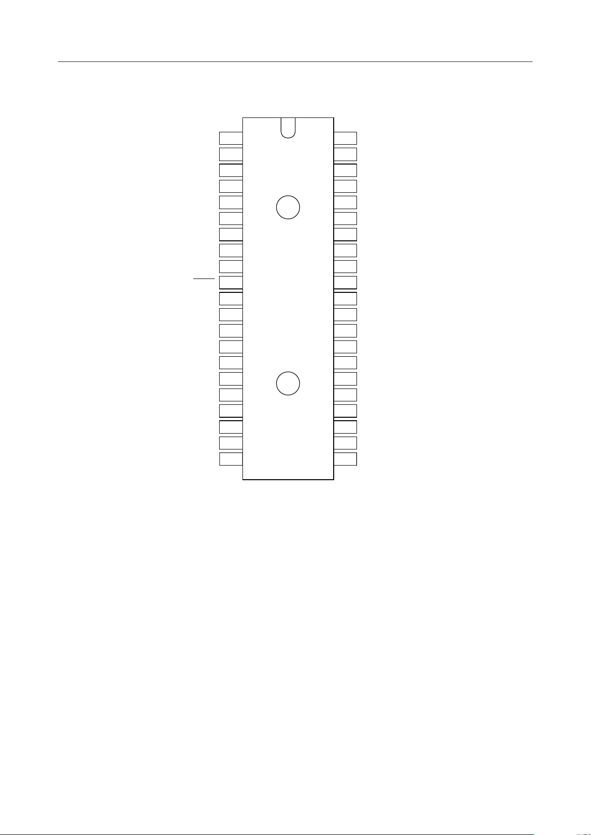
PIN CONFIGURATION (TOP VIEW)
MSM6408¡ Semiconductor
P4.0
P4.1
P4.2
P4.3
P3.0
P3.1
P3.2
P3.3
OSC
OSC
RESET
TEST
P2.0
P2.1
P2.2
P2.3
P0.0
P0.1
P0.2
P0.3
1
2
3
4
5
6
7
8
9
0
10
1
11
12
13
14
15
16
17
18
19
20
21GND P1.022
42
41
40
39
38
37
36
35
34
33
32
31
30
29
28
27
26
25
24
23
V
DD
P5.3
P5.2
P5.1
P5.0
P6.3
P6.2
P6.1
P6.0
P7.3
P7.2
P7.1
P7.0
P8.3
P8.2
P8.1
P8.0
P1.3
P1.2
P1.1
42-Pin Plastic DIP
3/19
Page 4
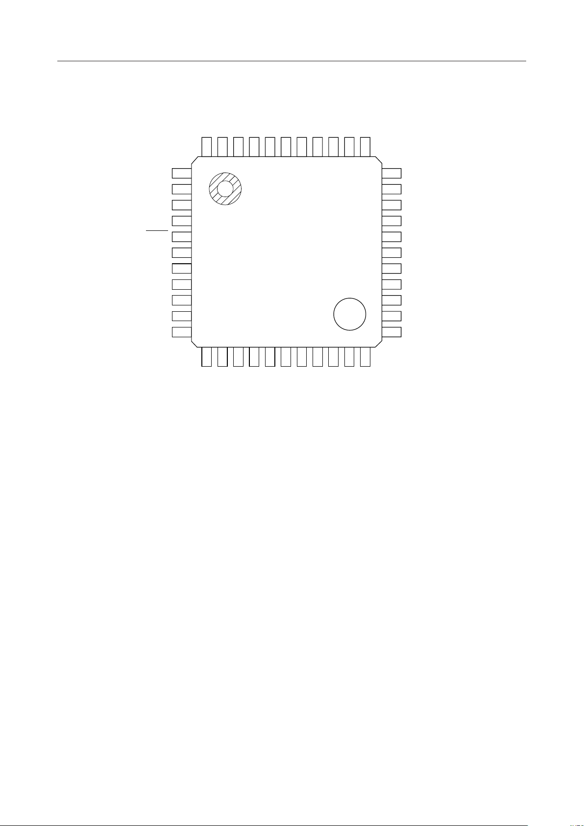
PIN CONFIGURATION (TOP VIEW) (continued)
MSM6408¡ Semiconductor
P3.1
P3.2
P3.3
OSC
OSC
RESET
TEST
P2.0
P2.1
P2.2
P2.3
P3.0
P4.3
P4.2
P4.1
44
43
42
41
1
2
3
4
0
5
1
6
7
8
9
10
11
12
13
14
15
P0.0
P0.1
P0.2
P0.3
P4.0
40
16
GND
DD
V
39
17
NC
P5.3
38
18
P1.0
P5.2
37
19
P1.1
P5.1
36
20
P1.2
P5.0
35
21
P1.3
P6.3
34
22
P8.0
33
32
31
30
29
28
27
26
25
24
23
P6.2
P6.1
P6.0
NC
P7.3
P7.2
P7.1
P7.0
P8.3
P8.2
P8.1
NC : No-connection pin
44-Pin Plastic QFP
4/19
Page 5
MSM6408¡ Semiconductor
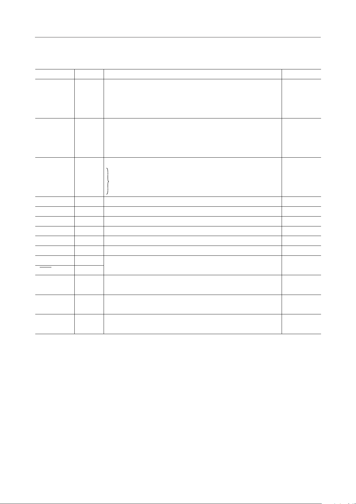
PIN DESCRIPTIONS
Symbol Type Description During reset
P0.0
P0.1/SCK
P0.2/SO
I/O
P0.3/SI
P1.0/CIN
P1.1/TMO P1.1 is shared with timer output (TMO).
P1.2/TCK
I/O
P1.3
P2.0/INT
P2.1
I
P2.3
P3.0 to 3.3
P4.0 to 4.3
P5.0 to 5.3
P6.0 to 6.3
P7.0 to 7.3
OSC
0
OSC
1
I/O
I/O
I/O
I/O
I/O
I/O
I
O
P0.1 is shared with serial clock (SLK) input/output.
P0.2 is shared with serial data (SO) output.
P0.3 is shared with serial data (SI) input.
P1.0 is shared with counter input (CIN).
P1.2 is shared with timer clock input (TCK).
P2.0 is shared with external interrupt input (INT).
Input ports with a latch, with built-in pull-up resistor.P2.2
—
—
—
—
—
—
Crystal connection pins for clock oscillation.
The latch is
reset.
Oscillation
waveform
"1"
"1"
"1"
"0"
"0"
"0"
"0"
"0"P8.0 to 8.3
TEST
RESET
V
DD
—
O
I
Input pin for system reset.
Power supply voltage pins.
GND
Note: 1. The pins except for pins P2.0 to P2.3 are pseudo bidirectional ports.
2. When each port is used for output, the MSM6408 can drive one TTL (one input).
Pulse output(Test pin for manufacturer)
—
—
5/19
Page 6
INSTRUCTION LIST
Mnemonic Byte DescriptionCode Cycle
LAI n 1 A¨n9n 1
LLI n 1 L¨n8n 1
LHLI nn 2 HL¨nn15nn 2
LMI nn 2 M(w)¨nn14nn 2
LAL 1 A¨L21 1
LLA 1 L¨A2D 1
LAH 1 A¨H22 1
LHA 1 H¨A2E 1
LAM 1 A¨M38 1
LMA 1 M¨A2F 1
LAM+ 1 A¨M, L¨L + 1,Skip if L = 024 1
LAM– 1 A¨M, L¨L – 1,Skip if L = F25 1
LMA+ 1 M¨A, L¨L + 1,Skip if L = 026 1
LMA– 1 M¨A, L¨L – 1,Skip if L = F27 1
Load, Push, PopExchange
LAMM n
LAMD mm 2 A¨Md10mm 2
LMAD mm 2 Md¨A11mm 2
LMTD mm 2 Md(w)¨T (M(w), A), T = ROM table19mm 3
LMCT 2 M(w)¨CT3E59 2
LCTM 2 CT¨M(w)3E51 2
LMSR 2 M(w)¨SR3E5A 2
LSRM 2 SR¨M(w)3E52 2
LTMM 2 TM¨(M(w), A)3E50 2
PUSH 1 ST¨C, A, H, L, SP¨SP – 41C 3
POP 1 C, A, H, L, ¨ST SP¨SP + 41D 3
X1A´M28 1
XM n
X+ 1 A´M, L¨L+1, Skip if L = 03C 1
X– 12C 1
INA 1 A¨A + 1, Skip if A = 030 1
INM 1 A¨M + 1, Skip if M = 033 1
INL 1 L¨L + 1, Skip if L = 031 1
Decrement
Increment/
2
2
39-3B 1
29-2B 1
1A¨M, H¨H n
1A´M, H¨H n
MSM6408¡ Semiconductor
2
2
A´M, L¨L–1, Skip if L = F
6/19
Page 7

INSTRUCTION LIST (continued)
Mnemonic Byte DescriptionCode Cycle
INH 1 H¨H + 1, Skip if M = 032 1
INMD mm 2 Md¨Md + 1, Skip if Md = 012mm 2
DCA 1 A¨A – 1, Skip if A = F34 1
DCM 1 M¨M – 1, Skip if M = F37 1
DCL 1 L¨L – 1, Skip if L = F35 1
DCH 1 H¨H – 1, Skip if H = F36 1
Increment/DecrementBit manipulation
DCMD mm 2 Md¨Md – 1, Skip if Md = F13mm 2
ADS 1 A¨A + M, Skip if Cy = 102 1
ADCS 1 A, C¨A + M + C, Skip if Cy =101 1
ADC 1 A, C¨A + M + C03 1
AIS n 2 A¨A + n, Skip if Cy = 13E4n 2
DAA 1 A¨A + 606 1
DAS 1 A¨A + 100A 1
AND 1 A¨A M0D 1
OR 1 A¨A M05 1
EOR 1 A¨A M04 1
ArithmeticCompare
CMA 1 A¨A0B 1
CIA 1 A¨A + 10C 1
RAL 1 Rotate left with C0E 1
RAR 1 Rotate right with C0F 1
TC 1 Skip if C = 109 1
SC 1 C¨107 1
RC 1 C¨008 1
CAI n 2 Skip if A = n3E0n 2
CLI n 2 Skip if L = n3E2n 2
CPI p, n 2 Skip if Pp = n17pn 2
CMI n 2 Skip if M = n3E1n 2
CAM 1 Skip if A = M16 1
TAB n
2
RAB n
2
SAB n
2
TMB n
2
RMB n
2
154-57 1
1 Abit (n2)¨064-67 1
1 Abit (n2)¨174-77 1
1 Skip if Mbit (n2) = 158-5B 1
1 Mbit (n2)¨068-6B 1
MSM6408¡ Semiconductor
Skip if Abit (n2) = 1
7/19
Page 8

INSTRUCTION LIST (continued)
Mnemonic Byte DescriptionCode Cycle
SMB n 1 Mbit (n
TFB n
2
RFB n
2
SFB n
2
TPB n
2
RPB n
2
SPB n
Bit manipulation
Interrupt
2
TPBD pn
RPBD pn
SPBD pn
2
2
2
0-3
4-7
MEI 2 MEIF¨13E60 2
MDI 2 MEIF¨03E61 2
EITB 2 EITBF¨13DC9 2
EITM 2 EITMF¨13DCA 2
EICT 2 EICTF¨13DCB 2
EIEX 2 EIEXF¨13DC8 2
DITB 2 EITBF¨03DC5 2
DITM 2 EITMF¨03DC6 2
DICT 2 EICTF¨03DC7 2
DIEX 2 EIEXF¨03DC4 2
TITB 2 Skip if EITBF = 13DC1 2
TITM 2 Skip if EITMF = 13DC2 2
TICT 2 Skip if EICTF = 13DC3 2
TIEX 2 Skip if EIEXF = 13DC0 2
TQEX 2 Skip if IRQEX = 13D20 2
TQTB 2 Skip if IRQTB = 13DD0 2
TQTM 2 Skip if IRQTM = 13DD1 2
TQCT 2 Skip if IRQCT = 13DD2 2
TQSR 23DD3 2
RQEX 23D24 2
RQTB 23DD4 2
RQTM 23DD5 2
RQCT 23DD6 2
RQSR 23DD7 2
)¨178-7B 1
2
1 Skip if Fbit (n2) = 15C-5F 1
1 Fbit (n2)¨06C-6F 1
1 Fbit (n2)¨17C-7F 1
1 Skip if Pbit (n2) = 150-53 1
1 Pbit (n2)¨060-63 1
1 Pbit (n2)¨170-73 1
2 Skip if Ppbit (n2) = 130 p
2 Ppbit (n2) = 03D p
2
2
2 Ppbit (n2) = 13D p8-B2
Skip if IRQSR = 1
IRQ EX¨0
IRQ TB¨0
IRQ TM¨0
IRQ CT¨0
IRQ SR¨0
MSM6408¡ Semiconductor
8/19
Page 9

INSTRUCTION LIST (continued)
Mnemonic Byte DescriptionCode Cycle
ECT 2 CTF¨1 (start)3DBB 2
ESR 2 SRF¨1 (start)3DBA 2
DCT 2 CTF¨0 (stop)3DB7 2
control
DSR 2 SRF¨0 (stop)3DB6 2
TCT 2 Skip if CTF = 13DB3 2
TSR 2 Skip if SRF = 13DB2 2
Counter/Shift register
JCP a
6
JP a
12
LJP a
13
CZP a 1 ST¨PC + 1, PC¨2a, SP¨SP – 4Ba 4
CAL a
Branch
12
RT 1 PC¨ST, SP¨SP + 4IE 4
RTS 1 PC¨ST, SP¨SP + 4, Unconditional skipIF 4
JA 1 PC¨(PC¨A) + 1IA 1
JM 1 PC¨(M(w), A)IB 2
IP 1 A¨P20 1
IPD p 2 A¨Pp3DpD 2
OP 1 P¨A23 1
Input/Output
OPD p 2 Pp¨A3DpC 2
NOP 1 No operation00 1
HALT 2 Halt CPU3DB8 2
CPU
control
STOP 2 Stop clock3DB9 2
C0-FF 1
4a
12
3F 4
12
1PC¨a
2PC¨a
2
3PC¨a
2ST¨PC + 2, PC¨a12, SP¨SP – 4Aa
4
MSM6408¡ Semiconductor
6
12
13
Notes: a : ROM address data
m : RAM address data
n : Immediate data
p : Port address data
9/19
Page 10

ABSOLUTE MAXIMUM RATINGS
Parameter Symbol Condition Rating Unit
Power Supply Voltage V
Input Voltage V
Output Voltage V
DD
I
O
Ta = 25°C
Ta = 25°C per package 200 mW
Power Dissipation P
Storage Temperature T
D
STG
Ta = 25°C per output 50 mW
— –55 to +150 °C
RECOMMENDED OPERATING CONDITIONS
Parameter Symbol Condition Range Unit
f
£ 1 MHz 3 to 6 V
Power Supply Voltage V
Data-Hold Voltage V
DDH
Operating Temperature T
Fan Out N
DD
op
OSC
f
£ 4.0 MHz
OSC
f
= 0 Hz 2 to 6
OSC
—
MOS load 15
TTL load 1
MSM6408¡ Semiconductor
–0.3 to +7 V
–0.3 to V
–0.3 to V
4.5 to 5.5 V
–40 to +85 °C
DD
DD
V
V
V
—
10/19
Page 11

ELECTRICAL CHARACTERISTICS
DC Characteristics
(V
= 5 V ±10%, Ta = –40 to +85°C)
DD
Parameter Symbol Condition Min. Typ. Max. Unit
"H" Input Voltage V
"H" Input Voltage V
"L" Input Voltage V
"H" Output Voltage V
"L" Output Voltage
"L" Output Voltage
Input Current I
Input Current — — 1/–30
"H" Output Current I
"H" Output Current
Input Capacitance C
Output Capacitance C
Power Supply Current
(In Stopped State)
Power Supply Current I
*1,*2
*3,*4
*1,*5
*1
*5
*3
*2,*4
*1
*1
V
V
IH/IIL
I
IH/IIL
OH
I
OH
I
DDS
DD
IH
IH
IL
OH
OL
OL
— 2.4 — V
— 3.6 — V
— –0.3 — +0.8 V
IO = –15 mA 4.2 — — V
IO = 1.6 mA — — 0.4 V
IO = 15 mA — — 0.4 V
VI = VDD/0 V — — 15/–15 mA
VI = VDD/0 V mA
VO = 2.4 V –0.1 — — mA
VO = 0.4 V — — –1.2 mA
I
O
f = 1 MHz, Ta = 25°C
V
= 2 V, no load, Ta = 25°C
DD
—5—
—7—
— 0.2 5 mA
No load — 1 100 mA
Crystal oscillation
f = 4 MHz, no load
—612mA
DD
DD
MSM6408¡ Semiconductor
V
V
pF
*1 Applied to P0, P1, P3, P4, P5, P6, P7 and P8
*2 Applied to P2
*3 Applied to OSC
0
*4 Applied to RESET
*5 Applied to OSC
1
11/19
Page 12

AC Characteristics
Parameter Symbol Condition Min. Typ. Max. Unit
Clock (OSC
Cycle Time t
Input Data Setup Time t
Input Data Hold Time t
SR/TM Clock Pulse Width t
CT Clock Pulse Width
P2 Input Data Clock Pulse Width t
SR Data Setup Time t
SR Data Hold Time t
Data Delay Time t
Data Delay Time at Mode
Switching
Data Delay Time at OPT
Instruction
Data Delay Time at OPT
Instruction
CT/TM Data Delay Time Using
TBC Clock
SR/TM Data Delay Time Using
PORT Clock
CT Data Delay Time Using
PORT Clock
CT Data Delay Time Using
External Clock
SR/TM Data Delay Time Using
External Clock
SR Clock Invalid Time
INT Invalid Time
) Pulse Width t
0
f
W
CY
DS
DH
WS/tWT
t
WC
WP
SS
SH
DR
t
DCR
t
DI1
t
DI2
t
CT/tTT
t
SR/tTR
t
CR
t
CP
t
SP/tTP
t
SINH
t
IINH
MSM6408¡ Semiconductor
= 5 V ±10%, Ta = –40 to +85°C)
(V
DD
— 125 — — ns
CY
m
ns
ns
ns
ns
ns
ns
—1——
— 120 — — ns
— 120 — — ns
— 120 — — ns
2/8 t
—
+ 120
CY
——ns
— 120 — — ns
— 120 — — ns
— 120 — — ns
CL = 15 pF — — t
CL = 15 pF — —
CL = 15 pF — —
CL = 15 pF — —
CL = 15 pF — —
+ 300 ns
CY
7/8 t
CY
+ 300
6/8 t
CY
+ 300
7/8 t
CY
+ 300
2/8 t
CY
+ 360
CL = 15 pF — — tCY + 480 ns
10/8 t
CL = 15 pF — —
CL = 15 pF — —
+ 480
2/8 t
+ 360
CY
CL = 15 pF — — 360 ns
— 2/8 t
— 1/8 t
CY
CY
——ns
——ns
s
12/19
Page 13

Timing Diagrams
Output Conditions
OSC
MSM6408¡ Semiconductor
1MC
0
t
CY
P0, P1, P3
P4, P5, P6 PA =
P7, P8
P0.1
PA = 9 or A
P0.2
P1.1
P4 OPT INST.
P5 OPT INST.
P0.1
TBC clock
P1.1
P0.1 clock*
P0.2
P1.2 clock* SRTM
P1.1
0, 1, 3
4
, 5, 6
7 or 8
CT
TM
t
DR
t
DCR
t
DI1
t
DI2
t
CT
t
TT
t
SR
t
TR
P1.0
P0.1
P0.1
P1.0
clock*CT
EXT clock
P1.2 EXT clock
P0.1 CT
P0.2 SR
P1.1 TM
t
SP
t
TP
* Output data to port is clock for SR, TM or CT.
t
CR
t
CP
13/19
Page 14

Input Conditions
OSC
MSM6408¡ Semiconductor
1MC
0
P0, P1, P2
P3, P4, P5
P6, P7, P8
P0.1 SR clock
P1.2 TM clock
P2
P1.0 CT clock
P0.1 SR clock
P0.3 SI
tfWtf
W
INPUT
DATA
tDSt
DH
t
DW1
t
DW2
INPUT
DATA
tSSt
SH
t
SINH
t
IINH
1MC
OSC
0
t
IINH
t
SINH
: P0.1 (SR clock) INH period during LMSR INST.
(Note: P0.1 is used for clock of SR.)
: P2.0 (interrupt) INH period during RPB and RPBD INST.
14/19
Page 15

Operating Characteristics
MSM6408¡ Semiconductor
Typ. Current (IOH) vs Voltage (VOH) for High
State Output
–1.0
–0.9
–0.8
–0.7
V
= 6 V
DD
–0.6
(mA)
–0.5
OH
I
–0.4
–0.3
–0.2
5 V
4 V
3 V
–0.1
0
012345678910
VOH (V) VOL (V)
Typ. Maximum Oscillator Frequnecy (f
Ta = 25°C
OSC
vs Supply Voltage (VDD)
10
(MHz)
OSC
f
9
8
7
6
5
4
3
2
1
0
012345678910
Ta = 25°C, CL = 15 pF
VDD (V)
Typ. Current (IOL) vs Voltage (VOL) for Low
State Output
20
18
6 V
V
DD
16
14
12
(mA)
10
OL
I
8
6
4 V
3 V
4
2
0
012345678910
)
Typ. Maximum Oscillator Frequnecy (f
= 5 V
Ta = 25°C
OSC
)
vs Temperature (Ta)
V
DD
CL = 15 pF
= 5 V
100
10
9
8
7
6
(MHz)
5
OSC
4
f
3
2
1
0
–40 –20 0 20 40 60 80 120
Ta (°C)
15/19
Page 16

Operating Characteristics (continued)
Typ. Supply Current (IDD) vs Supply Voltage (VDD)
MSM6408¡ Semiconductor
10 m
100 m
(A)
DD
I
10 m
100 n
Ta = 25°C, no load
f
OSC
2 MHz
1 MHz
1 m
500 kHz
100 kHz
0 Hz
1 m
012345678910
V
(V)
DD
= 4 MHz
16/19
Page 17

PACKAGE DIMENSIONS
DIP42-P-600-2.54
MSM6408¡ Semiconductor
(Unit : mm)
Package material
Lead frame material
Pin treatment
Solder plate thickness
Package weight (g)
Epoxy resin
42 alloy
Solder plating
5 mm or more
6.20 TYP.
17/19
Page 18

QFP44-P-910-0.80-K
Mirror finish
MSM6408¡ Semiconductor
(Unit : mm)
Package material
Lead frame material
Pin treatment
Solder plate thickness
Package weight (g)
Epoxy resin
42 alloy
Solder plating
5 mm or more
0.35 TYP.
Notes for Mounting the Surface Mount Type Package
The SOP, QFP, TSOP, SOJ, QFJ (PLCC), SHP and BGA are surface mount type packages, which
are very susceptible to heat in reflow mounting and humidity absorbed in storage.
Therefore, before you perform reflow mounting, contact Oki’s responsible sales person for the
product name, package name, pin number, package code and desired mounting conditions
(reflow method, temperature and times).
18/19
Page 19

QFP44-P-910-0.80-2K
Mirror finish
MSM6408¡ Semiconductor
(Unit : mm)
Package material
Lead frame material
Pin treatment
Solder plate thickness
Package weight (g)
Epoxy resin
42 alloy
Solder plating
5 mm or more
0.41 TYP.
Notes for Mounting the Surface Mount Type Package
The SOP, QFP, TSOP, SOJ, QFJ (PLCC), SHP and BGA are surface mount type packages, which
are very susceptible to heat in reflow mounting and humidity absorbed in storage.
Therefore, before you perform reflow mounting, contact Oki’s responsible sales person for the
product name, package name, pin number, package code and desired mounting conditions
(reflow method, temperature and times).
19/19
 Loading...