

Page 1

E2E0056-19-62
¡ Semiconductor MSM63188A
This version: Jun. 1999
¡ Semiconductor
MSM63188A
4-Bit Microcontroller with Built-in 1024-Dot Matrix LCD Drivers and Melody Circuit,
Operating at 0.9 V (Min.)
GENERAL DESCRIPTION
The MSM63188A is an enhanced version of the MSM63188 in which supply currents have been
improved.
The MSM63188A is a CMOS 4-bit microcontroller with built-in 1024-dot matrix LCD drivers and
operates at 0.9 V (min.). The MSM63188A is suitable for applications such as games, toys,
watches, etc. which are provided with an LCD display.
The MSM63188A is an M6318x series mask ROM-version product of OLMS-63K family, which
employs Oki's original CPU core nX-4/250.
The MSM63P180 is the one-time-programmable ROM version of MSM63188/A, having one-time
PROM (OTP) as internal program memory.
The MSM63P180 is used to evaluate the software development.
FEATURES
• Rich instruction set
439 instructions
Transfer, rotate, increment/decrement, arithmetic operations, comparison, logic operations,
mask operations, bit operations, ROM table reference, external memory transfer, stack
operations, flag operations, branch, conditional branch, call/return, control.
• Rich selection of addressing modes
Indirect addressing of four data memory types, with current bank register, extra bank
register, HL register and XY register.
Data memory bank internal direct addressing mode.
• Processing speed
Two clocks per machine cycle, with most instructions executed in one machine cycle.
Minimum instruction execution time : 61 ms (@ 32.768 kHz system clock)
1 ms (@ 2 MHz system clock)
• Clock generation circuit
Low-speed clock : 32.768 kHz crystal oscillator
High-speed clock : 2 MHz (Max.) RC or ceramic oscillator select
• Program memory space
16K words
Basic instruction length is 16 bits/1 word
• Data memory space
3584 nibbles
• External data memory space
64 Kbytes (expandable by using an I/O port)
1/32
Page 2

¡ Semiconductor MSM63188A
• Stack level
Call stack level : 16 levels
Register stack level : 16 levels
• I/O ports
Input ports: Selectable as input with pull-up resistance/input with pull-down resistance/
high-impedance input
Output ports: Selectable as P-channel open drain output/N-channel open drain output/
CMOS output/high-impedance output
Input-output ports: Selectable as input with pull-up resistance/input with pull-down
resistance/high-impedance input
Selectable as P-channel open drain output/N-channel open drain
output/CMOS output/high-impedance output
Can be interfaced with external peripherals that use a different power supply than this device
uses.
Number of ports:
Input port : 2 ports ¥ 4 bits
Output port : 6 ports ¥ 4 bits
Input-output port : 6 ports ¥ 4 bits
• Melody output function
Melody sound frequency : 529 to 2979 Hz
Tone length : 63 types
Tempo : 15 types
Note data : Resides in the program memory
Buzzer drive signal output : 4 kHz
• LCD driver
Number of segments : 1024 Max. (64 SEG ¥ 16 COM)
1/1 to 1/16 duty
1/4 or 1/5 bias (regulator built-in)
Selectable as all-on mode/all-off mode/power down mode/normal display mode
Adjustable contrast
• Multiplier/divider circuits
Multiplier : (8 bits) ¥ (8 bits) Æ Product (16 bits)
Divider : (16 bits) ÷ (8 bits) Æ Quotient (16 bits), Remainder (8 bits)
• Reset function
Reset through RESET pin
Power-on reset
Reset by low-speed oscillation halt
• Battery check
Low-voltage supply check
Criterion voltage : Can be selected as 1.05 ±0.10 V, 1.30 ±0.15 V,
2.20 ±0.20 V or 2.80 ±0.30 V
• Power supply backup
Backup circuit (voltage multiplier) enables operation at 0.9 V minimum
2/32
Page 3

¡ Semiconductor MSM63188A
• Timers and counter
8-bit timer ¥ 4
Selectable as auto-reload mode/capture mode/clock frequency measurement mode
Watchdog timer ¥ 1
Overflows in 2 sec.
100 Hz timer ¥ 1
Measurable in steps of 1/100 sec.
15-bit time base counter ¥ 1
1, 2, 4, 8, 16, 32, 64, and 128 Hz signals can be read
• Serial port
Mode : UART mode, synchronous mode
UART communication speed : 1200 bps, 2400 bps, 4800 bps, 9600 bps
Clock frequency in synchronous mode : 32.768 kHz (internal clock mode), external
clock frequency
Data length : 5 to 8 bits
• Interrupt sources
External interrupt : 4
Internal interrupt : 13 (watchdog timer interrupt is a nonmask-
able interrupt)
• Operating voltage
When backup used : 0.9 to 2.7 V
(Low-speed clock operating)
1.2 to 2.7 V
(Operating frequency: 300 to 500 kHz)
1.5 to 2.7 V
(Operating frequency: 200 kHz to 1 MHz)
When backup not used : 1.8 to 5.5 V
(Operating frequency: 300 to 500 kHz)
2.2 to 5.5 V
(Operating frequency: 300 kHz to 1 MHz)
2.7 to 5.5 V
(Operating frequency: 200 kHz to 2 MHz)
• Package:
176-pin plastic LQFP (LQFP176-P-2424-0.50-BK) : (Product name: MSM63188A-xxxGS-BK)
Chip : (Product name: MSM63188A-xxx)
xxx indicates a code number.
Differences Between the MSM63188 and the MSM63188A
The MSM63188A has the following improved characteristics.
• Supply currents (I
• The V
voltage during a halt of high-speed clock oscillation
DDL
DD1
, I
DD2
, I
) in DC characteristics
DD3
3/32
Page 4
¡ Semiconductor MSM63188A
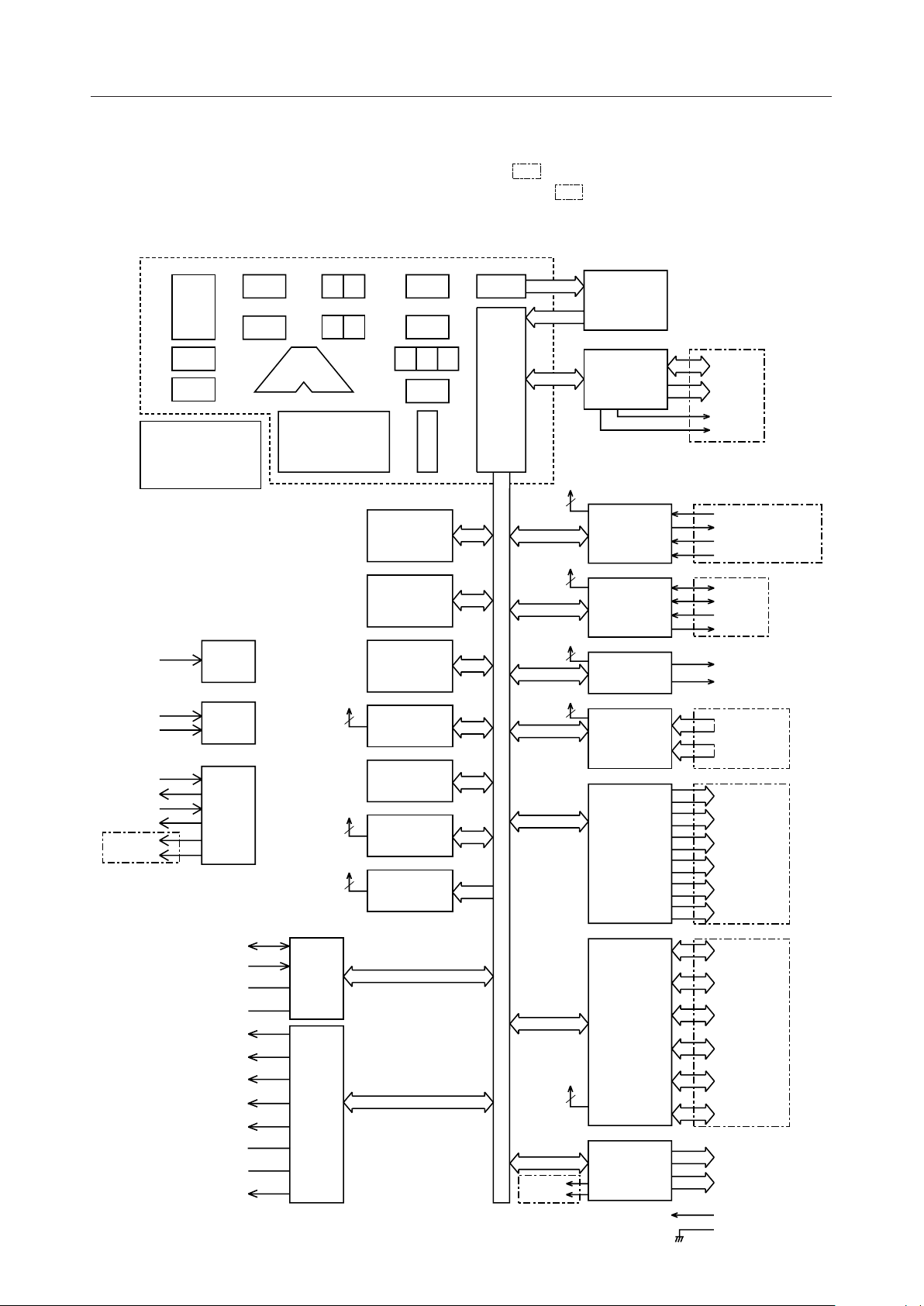
BLOCK DIAGRAM
An asterisk (*) indicates the port secondary function. indicates that the power is supplied
to the circuits corresponding to the signal names inside from V
interface).
nX-4/250
H
RESET
TST1
TST2
TIMING
CONTROL
SP
RSP
STACK
CAL : 16-level
REG : 16-level
RST
TST
CBR
EBR
ALU
INSTRUCTION
DECODER
4
INT
L
YX
C G
RAM
3584N
INT188
MULDIV
TBC
RA
A
Z
MIE
IR
PC
BUS
CONTROL
DATA BUS
ROM
16KW
EXTMEM
INT
4
TIMER
8bit ¥ 4
INT
2
SIO
INT
1
MELODY
INT
1
INPUT
PORT
(power supply for
DDI
D0-7*
A0-15*
RD*
WR*
TM0CAP/TM1CAP*
TM0OVF/TM1OVF*
T02CK*
T13CK*
RXC*
TXC*
RXD*
TXD*
MD
MDB
P0.0-P0.3
P1.0-P1.3
XT0
XT1
OSC0
OSC1
TBCCLK*
HSCLK*
OSC
V
CB1
CB2
V
V
V
V
V
V
DDH
V
DD1
DD2
DD3
DD4
DD5
DDL
DD
C1
C2
BACK
UP
BIAS
BLD
INT
1
INT
1
100HzTC
WDT
LCLK*
FRAME*
OUTPUT
PORT
I/O
PORT
INT
3
LCD
&
DSPR
P2.0-P2.3
P3.0-P3.3
P4.0-P4.3
P5.0-P5.3
P6.0-P6.3
P7.0-P7.3
P8.0-P8.3
P9.0-P9.3
PA.0-PA.3
PB.0-PB.3
PC.0-PC.3
PD.0-PD.3
COM1-16
SEG0-63
V
DDI
V
SS
4/32
Page 5
¡ Semiconductor MSM63188A
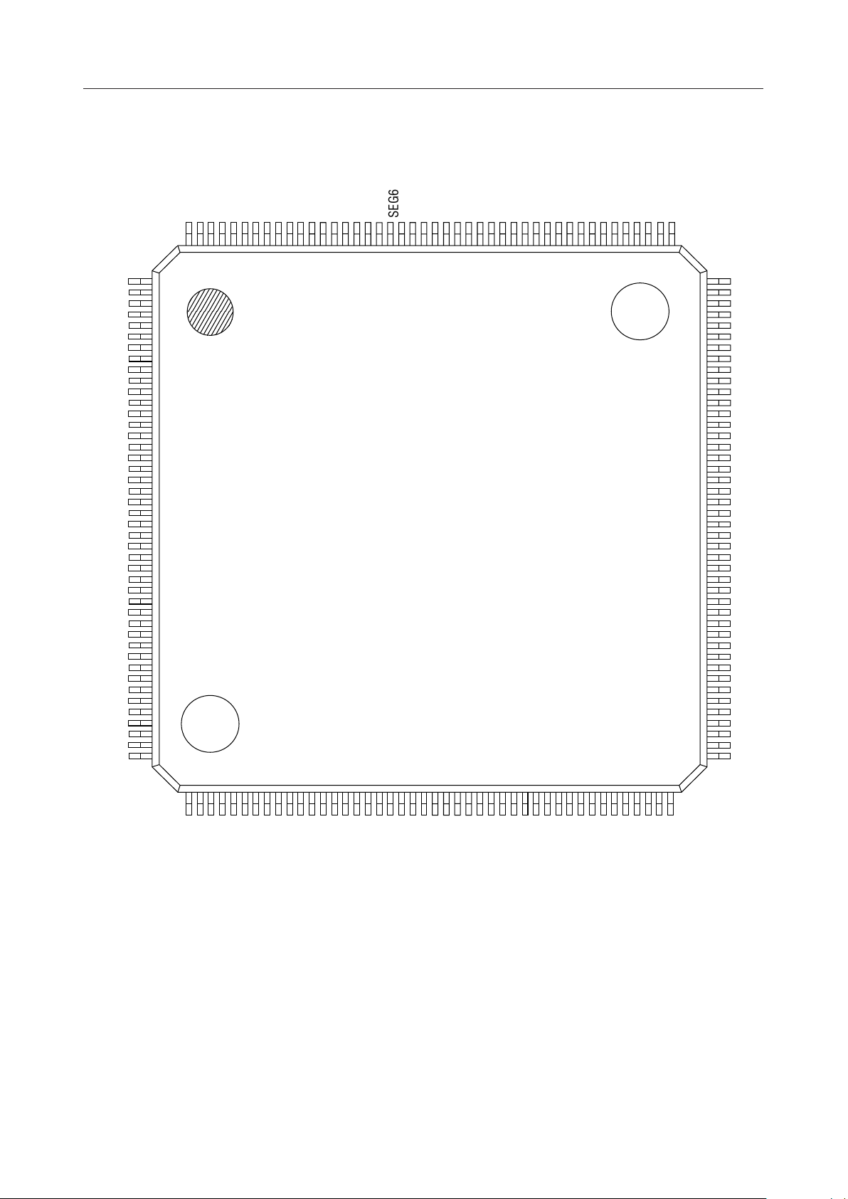
PIN CONFIGURATION (TOP VIEW)
SEG61
SEG62
SEG63
(NC)
P0.0
P0.1
P0.2
P0.3
P1.0
P1.1
P1.2
P1.3
P2.0
P2.1
P2.2
P2.3
P3.0
P3.1
P3.2
P3.3
P4.0
P4.1
P4.2
P4.3
(NC)
SEG43
SEG42
SEG41
SEG40
SEG39
SEG38
SEG37
SEG36
SEG35
SEG34
SEG33
SEG32
SEG31
SEG30
SEG29
SEG28
SEG27
SEG26
SEG25
SEG24
SEG23
SEG22
SEG21
SEG20
SEG19
SEG18
SEG17
SEG16
SEG15
SEG14
SEG13
SEG12
SEG11
SEG10
SEG9
SEG8
SEG7
SEG6
SEG5
SEG4
SEG3
SEG2
SEG1
SEG0
11
2
3
4
5
6
7
8
9
10
11
12
13
14
15
16
17
18
19
20
21
22
23
24
25
26
27
28
29
30
31
32
33
34
35
36
37
38
39
40
41
42
43
44
SEG45
SEG46
SEG47
SEG48
SEG49
SEG50
SEG51
SEG52
SEG53
168
167
SEG54
166
165
(NC)
SEG44
174
173
172
171
170
176
175
474849505152535455565758596061
45
46
169
SEG55
SEG56
SEG57
164
163
162
SEG58
SEG59
SEG60
158
157
156
155
154
153
152
151
150
149
148
147
146
145
144
143
142
141
161
160
159
63646566676869707172737475767778798081828384858687
62
140
139
138
137
136
135
134
(NC)
133
132
131
130
129
128
127
126
125
124
123
122
121
120
119
118
117
116
115
114
113
112
111
110
109
108
107
106
105
104
103
102
101
100
99
98
97
96
95
94
93
92
91
90
89
88
P5.0
P5.1
P5.2
P5.3
P6.0
P6.1
P6.2
P6.3
P7.0
P7.1
P7.2
P7.3
P8.0
P8.1
P8.2
P8.3
P9.0
P9.1
P9.2
P9.3
PA.0
PA.1
PA.2
PA.3
PB.0
PB.1
PB.2
PB.3
PC.0
PC.1
PC.2
PC.3
PD.0
PD.1
PD.2
PD.3
(NC)
(NC)
(NC)
(NC)
(NC)
(NC)
(NC)
(NC)
(NC)
COM16
COM15
COM14
COM13
COM12
COM11
COM10
COM9
COM8
COM7
COM6
COM5
COM4
COM3
COM2
SS
DD1VDD2VDD3VDD4VDD5
V
V
COM1
C1
C2
DDH
V
CB1
CB2
DD
DDL
V
V
OSC1
OSC0
XT1
XT0
RESET
TST2
176-Pin Plastic LQFP
Note: Pins marked as (NC) are no-connection pins which are left open.
(NC)
TST1
MD
(NC)
(NC)
MDB
V
DDI
(NC)
5/32
Page 6
¡ Semiconductor MSM63188A
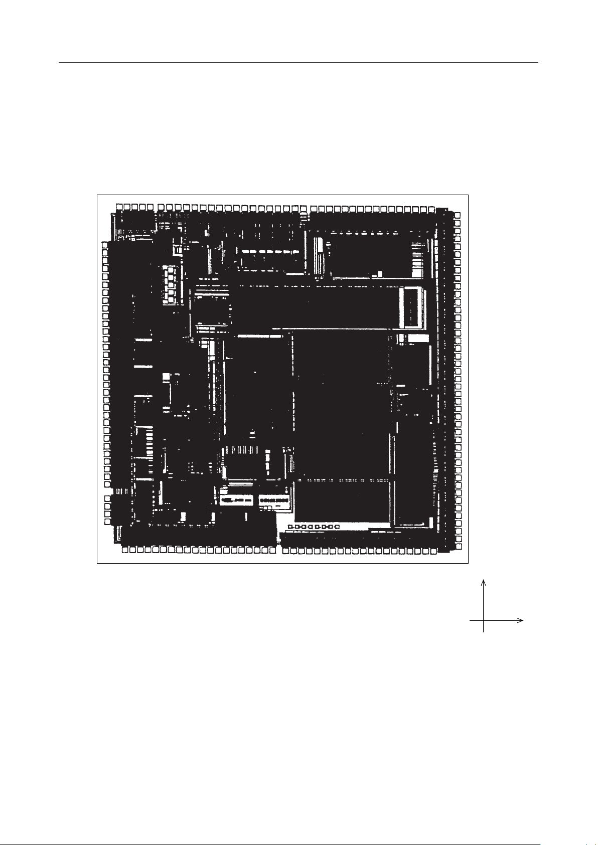
PAD CONFIGURATION
Pad Layout
PD.3
PD.2
PD.1
PD.0
PC.3
PC.2
PC.1
PC.0
PB.3
PB.2
PB.1
PB.0
PA.3
PA.2
PA.1
PA.0
P9.3
P9.2
P9.1
P9.0
P8.3
P8.2
P8.1
P8.0
P7.3
P7.2
P7.1
P7.0
P6.3
P6.2
P6.1
P6.0
P5.3
P5.2
P5.1
P5.0
124
125
126
127
128
129
130
131
132
133
134
135
136
137
138
139
140
141
142
143
144
145
146
147
148
149
150
151
152
153
154
155
156
157
158
159
DDI
122 MDB
121 MD
123 V
118 XT0
117 XT1
119 TST2
120 TST1
DDL
116 RESET
112 V
113 V
115 OSC0
114 OSC1
DD
110 CB1
111 CB2
DDH
108 C2
109 V
DD5
DD4
106 V
105 V
107 C1
DD3
DD2
104 V
103 V
DD1
SS
102 V
101 V
100 COM1
98 COM3
97 COM4
99 COM2
96 COM5
93 COM8
95 COM6
92 COM9
94 COM7
89 COM12
91 COM10
87 COM14
88 COM13
90 COM11
85 COM16
86 COM15
84 SEG0
83 SEG1
82 SEG2
81 SEG3
80 SEG4
79 SEG5
78 SEG6
77 SEG7
76 SEG8
75 SEG9
74 SEG10
73 SEG11
72 SEG12
71 SEG13
70 SEG14
69 SEG15
68 SEG16
67 SEG17
66 SEG18
65 SEG19
64 SEG20
63 SEG21
62 SEG22
61 SEG23
60 SEG24
59 SEG25
58 SEG26
57 SEG27
56 SEG28
55 SEG29
54 SEG30
53 SEG31
52 SEG32
51 SEG33
50 SEG34
49 SEG35
48 SEG36
47 SEG37
46 SEG38
45 SEG39
44 SEG40
43 SEG41
42 SEG42
41 SEG43
Y
P4.3 1
P4.2 2
P4.1 3
P4.0 4
P3.3 5
P3.2 6
P3.1 7
P3.0 8
P2.3 9
P2.2 10
P2.1 11
P2.0 12
P1.3 13
P1.2 14
P1.1 15
P1.0 16
P0.3 17
P0.2 18
P0.1 19
P0.0 20
SEG63 21
SEG62 22
SEG61 23
SEG60 24
SEG59 25
SEG58 26
SEG57 27
SEG56 28
SEG55 29
SEG54 30
SEG53 31
SEG52 32
SEG51 33
SEG50 34
SEG49 35
SEG48 36
SEG47 37
SEG46 38
SEG45 39
SEG44 40
X
Chip Size : 6.60 mm ¥ 6.60 mm
Chip Thickness : 350 mm (typ.)
Coordinate Origin : Chip center
Pad Hole Size : 100 mm ¥ 100 mm
Pad Size : 110 mm ¥ 110 mm
Minimum Pad Pitch : 140 mm
Note: The chip substrate voltage is VSS.
6/32
Page 7
¡ Semiconductor MSM63188A
Pad Coordinates
Pad No.
Name
X (µm) Y (µm)
1 P4.3 –2837 –3105
Pad
2 –2697
3 –2557
4 –2417
5 –2277
6 –2137
7 –1997
8 –1857
9 –1717
10 –1577
11 –1437
12 –1297
13 –1157
14 –1017
15 –877
16 –737
17 –597
18 –457
19 –317
20 –177
21 54
22 194
P4.2 –3105 SEG41 3155
P4.1 –3105 SEG40 3155
P4.0 –3105 SEG39 3155
P3.3 –3105 SEG38 3155
P3.2 –3105 SEG37 3155
P3.1 –3105 SEG36 3155
P3.0 –3105 SEG35 3155
P2.3 –3105 SEG34 3155
P2.2 –3105 SEG33 3155
P2.1 –3105 SEG32 3155
P2.0 –3105 SEG31 3155
P1.3 –3105 SEG30 3155
P1.2 –3105 SEG29 3155
P1.1 –3105 SEG28 3155
P1.0 –3105 SEG27 3155
P0.3 –3105 SEG26 3155
P0.2 –3105 SEG25 3155
P0.1 –3105 SEG24 3155
P0.0 –3105 SEG23 3155
SEG63
SEG62
23 SEG61 334
24 SEG60 474
25 SEG59 614
26 SEG58 754
27 SEG57 894
28 SEG56 1034
29 SEG55 1174
30 SEG54 1314
31 SEG53 1454
32 SEG52 1594
33 SEG51 1734
34 SEG50 1874
35 SEG49 2014
36 SEG48 2154
37 SEG47 2294
38 SEG46 2434
39 SEG45 2574
40 SEG44 2714
41 SEG43 3155
Pad No.
42
Name
SEG42 3155 –2870
X (µm) Y (µm)
43
44
45
46
47
48
49
50
51
52
53
54
55
56
57
58
59
60
61
Pad
–3105 SEG22 3155
–3105 SEG21 3155
–3105 SEG20 3155
–3105 SEG19 3155
–3105 SEG18 3155
–3105 SEG17 3155
–3105 SEG16 3155
–3105 SEG15 3155
–3105 SEG14 3155
–3105 SEG13 3155
–3105 SEG12 3155
–3105 SEG11 3155
–3105 SEG10 3155
–3105 SEG9 3155
–3105 SEG8 3155
–3105 SEG7 3155
–3105 SEG6 3155
–3105 SEG5 3155
–3105 SEG4 3155
–3105 SEG3 3155
–3010 SEG2 3155
62
63
64
65
66
67
68
69
70
71
72
73
74
75
76
77
78
79
80
81
82
–2730
–2590
–2450
–2310
–2170
–2030
–1890
–1750
–1610
–1470
–1330
–1190
–1050
–910
–770
–630
–490
–350
–210
–70
70
210
350
490
630
770
910
1050
1190
1330
1470
1610
1750
1890
2030
2170
2310
2450
2590
2730
Pad No.
83
84
85
86
87
88
89
90
91
92
93
94
95
96
97
98
99
100
101
102
103
104
105
106
107
108
109
110
111
112
113
114
115
116
117
118
119
120
121
122
123
Pad
Name
X (µm) Y (µm)
SEG1 3155 2870
SEG0 3155
COM16
COM15
COM14
COM13
COM12
COM11
COM10
COM9 3105
COM8 3105
COM7 3105
COM6 3105
COM5 3105
COM4 3105
COM3 3105
COM2 3105
COM1 3105
V
SS
V
DD1
V
DD2
V
DD3
V
DD4
V
DD5
C1
C2
V
DDH
CB1
CB2
V
DD
V
DDL
OSC1
OSC0
RESET
XT1
XT0
TST2
TST1
MD
MDB
V
DDI
2705
2565
2425
2285
2145
2005
1865
1725
1585
1445
1305
1165
1025
885
745
605
420
270
120
–30
–179
–329
–479
–629
–779
–929
–1079
–1229
–1379
–1529
–1679
–1829
–1979
–2129
–2324
–2464
–2604
–2744
–2884
3010
3105
3105
3105
3105
3105
3105
3105
3105
3105
3105
3105
3105
3105
3105
3105
3105
3105
3105
3105
3105
3105
3105
3105
3105
3105
3105
3105
3105
3105
3105
7/32
Page 8
¡ Semiconductor MSM63188A
Pad Coordinates (continued)
Pad No.
124 PD.3 –3155 2428
125
126
127
128
129
130
131
132
133
134
135
Pad
Name
PD.2 2288
PD.1 2148
PD.0
PC.3
PC.2
PC.1
PC.0
PB.3
PB.2
PB.1
PB.0
X (µm) Y (µm)
–3155 –3155 –3155
–3155 –3155 –3155
–3155 –3155 –3155
–3155 –3155 –3155
–3155 –3155 –3155
–3155 –3155 –3155
–3155 –3155 –3155
–3155 –3155 –3155
–3155 –3155 –3155
–3155 –3155 –3155
–3155 –3155 –3155
2008
1868
1728
1588
1448
1308
1168
1028
888
Pad No.
136
137
138
139
140
141
142
143
144
145
146
147
Pad
Name
PA.3
PA.2
PA.1
PA.0
P9.3
P9.2
P9.1
P9.0
P8.3
P8.2
P8.1
P8.0
X (µm) Y (µm)
–3155 748
608
468
328
188
48
–92
–232
–372
–512
–652
–792
Pad No.
149
150
151
152
153
154
155
156
157
158
159
Pad
Name
P7.3
P7.2
P7.1
P7.0
P6.3
P6.2
P6.1
P6.0
P5.3
P5.2
P5.1
P5.0
X (µm) Y (µm)
–3155 –932148
–1072
–1212
–1352
–1492
–1632
–1772
–1912
–2172
–2312
–2452
–2592
8/32
Page 9
¡ Semiconductor MSM63188A
PIN DESCRIPTIONS
The basic functions of each pin of the MSM63188A are described in Table 1.
A symbol with a slash (/) denotes a pin that has a secondary function.
Refer to Table 2 for secondary functions.
For type, "—" denotes a power supply pin, "I" an input pin, "O" an output pin, and "I/O" an inputoutput pin.
Table 1 Pin Descriptions (Basic Functions)
Function Symbol Pin Type
73 —
62 —
63
64
65 —
66
67
V
V
V
V
V
V
V
DD
SS
DD1
DD2
DD3
DD4
DD5
C1 68 —
Power
Supply
C2 69 —
V
V
V
DDI
DDL
DDH
87 —
74 —
70 —
CB1 71 —
CB2 72 —
XT0 79 I
XT1 78 O
Oscillation
OSC0 76 I
OSC1 75 O
TST1 81 I
Test
TST2 80 I
Reset RESET 77 I
Description
Positive power supply
Negative power supply
Power supply pins for LCD bias (internally generated).
Capacitors (0.1 mF) should be connected between these pins and
V
.
SS
Capacitor connection pins for LCD bias generation.
A capacitor (0.1 mF) should be connected between C1 and C2.
Positive power supply pin for external interface
(power supply for input, output, and input-output ports)
Positive power supply pin for internal logic (internally generated).
A capacitor (0.1 mF) should be connected between this pin and V
SS
.
Voltage multiplier pin for power supply backup (internally generated).
A capacitor (1.0 mF) should be connected between this pin and VSS.
Pins to connect a capacitor for voltage multiplier.
A capacitor (1.0 mF) should be connected between CB1 and CB2.
Low-speed clock oscillation pins.
A 32.768 kHz crystal should be connected between XT0 and XT1,
(5 to 25 pF) should be connected between XT0 and VSS.
and C
G
High-speed clock oscillation pins.
A ceramic resonator and capacitors (C
oscillation resistor (R
) should be connected to these pins.
OS
, CL1) or external
L0
Input pins for testing.
A pull-down resistor is internally connected to these pins.
The user cannot use these pins.
Reset input pin.
Setting this pin to "H" level puts this device into a reset state.
Then, setting this pin to "L" level starts executing an instruction
from address 0000H.
A pull-down resistor is internally connected to this pin.
Melody
MD 84 O
MDB 85 O
Melody output pin (non-inverted output)
Melody output pin (inverted output)
9/32
Page 10
¡ Semiconductor MSM63188A
Table 1 Pin Descriptions (Basic Functions) (continued)
Function Symbol
P0.0/INT5
P0.1/INT5
P0.2/INT5
P0.3/INT5
P1.0/INT5
P1.1/INT5
P1.2/INT5
P1.3/INT5
P2.0
P2.1
P2.2
P2.3
P3.0
P3.1
P3.2
Port
P3.3
P4.0/A0
P4.1/A1
P4.2/A2
P4.3/A3
P5.0/A4
P5.1/A5
P5.2/A6
P5.3/A7
P6.0/A8
P6.1/A9
P6.2/A10
P6.3/A11
P7.0/A12
P7.1/A13
P7.2/A14
P7.3/A15
Pin
154
153
152
151
150
149
148
147
146
145
144
143
142
141
140
139
138
137
136
135
132
131
130
129
128
127
126
125
124
123
122
121
Type Description
4-bit input ports.
Pull-up resistor input, pull-down resistor input, or
I
high-impedance input is selectable for each bit.
I
4-bit output ports.
P-channel open drain output, N-channel open drain output,
O
CMOS output, or high-impedance output is selectable for each
bit.
O
O
O
O
O
10/32
Page 11

¡ Semiconductor MSM63188A
Table 1 Pin Descriptions (Basic Functions) (continued)
Function Symbol
P8.0/RD
P8.1/WR
P8.2
P8.3/INT4
P9.0/D0
P9.1/D1
P9.2/D2
P9.3/D3
PA.0/D4
PA.1/D5
PA.2/D6
PA.3/D7
PB.0/INT0/
Port
TM0CAP/
TM0OVF
PB.1/INT0/
TM1CAP/
TM1OVF
PB.2/INT0/T02CK
PB.3/INT0/T13CK
PC.0/INT1/RXD
PC.1/INT1/TXC
PC.2/INT1/RXC
PC.3/INT1/TXD
PD.0/FRAME
PD.1/LCLK
PD.2/TBCCLK
PD.3/HSCLK
Pin
120
119
118
117
116
115
114
113
112
111
110
109
108
107
106
105
104
103
102
101
100
99
98
97
Type Description
4-bit input-output ports.
In input mode, pull-up resistor input, pull-down resistor input,
I/O
or high-impedance input is selectable for each bit.
In output mode, P-channel open drain output, N-channel open
drain output, CMOS output, or high-impedance output is
selectable for each bit.
I/O
I/O
I/O
I/O
I/O
11/32
Page 12

¡ Semiconductor MSM63188A
Table 1 Pin Descriptions (Basic Functions) (continued)
Function Symbol
COM1
COM2
COM3
COM4
COM5
COM6
COM7
COM8
COM9
COM10
COM11
COM12
COM13
COM14
COM15
COM16
SEG0
SEG1
SEG2
SEG3
LCD
SEG4
SEG5
SEG6
SEG7
SEG8
SEG9
SEG10
SEG11
SEG12
SEG13
SEG14
SEG15
SEG16
SEG17
SEG18
SEG19
SEG20
SEG21
SEG22
SEG23
SEG24
Pin Type
61
60
59
58
57
56
55
54
53
52
51
50
49
48
47
46
44
43
42
41
40
39
38
37
36
35
34
33
32
31
30
29
28
27
26
25
24
23
22
21
20
O
O
Description
LCD common signal output pins
LCD segment signal output pins
12/32
Page 13

¡ Semiconductor MSM63188A
Table 1 Pin Descriptions (Basic Functions) (continued)
Function Symbol
SEG25
SEG26
SEG27
SEG28
SEG29
SEG30
SEG31
SEG32
SEG33
SEG34
SEG35
SEG36
SEG37
SEG38
SEG39
SEG40
SEG41
SEG42
SEG43
LCD
SEG44
SEG45
SEG46
SEG47
SEG48
SEG49
SEG50
SEG51
SEG52
SEG53
SEG54
SEG55
SEG56
SEG57
SEG58
SEG59
SEG60
SEG61
SEG62
SEG63
Pin Type
19
18
17
16
15
14
13
12
11
10
9
8
7
6
5
4
3
2
1
O
175
174
173
172
171
170
169
168
167
166
165
164
163
162
161
160
159
158
157
156
Description
LCD segment signal output pins
13/32
Page 14

¡ Semiconductor MSM63188A
Table 2 shows the secondary functions of each pin of the MSM63188A.
Table 2 Pin Descriptions (Secondary Functions)
Function Symbol
PB.0/INT0
PB.1/INT0
PB.2/INT0
PB.3/INT0
PC.0/INT1
PC.1/INT1
PC.2/INT1
External
Interrupt
PC.3/INT1
P8.3/INT4
P0.0/INT5
P0.1/INT5
P0.2/INT5
P0.3/INT5
P1.0/INT5
P1.1/INT5
P1.2/INT5
P1.3/INT5
Pin
108
107
106
105
104
103
102
101
117
154
153
152
151
150
149
148
147
Type Description
External 0 interrupt input pins.
The change of input signal level causes an interrupt to occur.
I
The Port B Interrupt Enable register (PBIE) enables or disables
an interrupt for each bit.
External 1 interrupt input pins.
The change of input signal level causes an interrupt to occur.
I
The Port C Interrupt Enable register (PCIE) enables or disables
an interrupt for each bit.
External 4 interrupt input pins.
I
The change of input signal level causes an interrupt to occur.
External 5 interrupt input pins.
The change of input signal level causes an interrupt to occur.
The Port 0 Interrupt Enable register (P0IE) and Port 1 Interrupt
Enable register (P1IE) enable or disable an interrupt for each bit.
I
14/32
Page 15

¡ Semiconductor MSM63188A
Table 2 Pin Descriptions (Secondary Functions) (continued)
Function Symbol
Capture
Timer
LCD
External
Expansion
Oscillation
Output
Serial
Port
PB.0/TM0CAP
PB.1/TM1CAP
PB.0/TM0OVF
PB.1/TM1OVF
PB.2/T02CK
PB.3/T13CK
PD.0/FRAME
PD.1/LCLK
PD.2/TBCCLK
PD.3/HSCLK
PC.0/RXD
PC.1/TXC
PC.2/RXC
PC.3/TXD
Pin
108
107
108
107
106
105
100
99
98
97
104
103
102
101
Type Description
Timer 0 capture input pin.
I
Timer 1 capture input pin.
I
Timer 0 overflow flag output pin.
O
Timer 1 overflow flag output pin.
O
External clock input pin for timer 0 and timer 2.
I
External clock input pin for timer 1 and timer 3.
I
Frame output pin for LCD driver expansion
O
Clock output pin for LCD driver expansion
O
Low-speed oscillation clock output pin
O
High-speed oscillation clock output pin
O
Serial port receive data input pin
I
Sync serial port clock input-output pin.
Transmit clock output when this device is used as a master processor.
I/O
Transmit clock input when this device is used as a slave processor.
Sync serial port clock input-output pin.
I/O
Receive clock output when this device is used as a master processor.
Receive clock input when this device is used as a slave processor.
Serial port transmit data output pin.
O
15/32
Page 16

¡ Semiconductor MSM63188A
Table 2 Pin Descriptions (Secondary Functions) (continued)
Function Symbol
P4.0/A0
P4.1/A1
P4.2/A2
P4.3/A3
P5.0/A4
P5.1/A5
P5.2/A6
P5.3/A7
P6.0/A8
P6.1/A9
P6.2/A10
P6.3/A11
External
P7.0/A12
Memory
P7.1/A13
P7.2/A14
P7.3/A15
P9.0/D0
P9.1/D1
P9.2/D2
P9.3/D3
PA.0/D4
PA.1/D5
PA.2/D6
PA.3/D7
P8.0/RD
P8.1/WR
Pin
138
137
136
135
132
131
130
129
128
127
126
125
124
123
122
121
116
115
114
113
112
111
110
109
120
119
Type
Address output bus for external memory
O
Data bus for external memory
I/O
O Read signal output pin for external memory (negative logic)
O Write signal output pin for external memory (negative logic)
Description
16/32
Page 17

¡ Semiconductor MSM63188A
ABSOLUTE MAXIMUM RATINGS
= 0 V)
(V
SS
Parameter Symbol Condition Rating Unit
Power Supply Voltage 6
DD1
V
DD2
V
DD3
V
DD4
V
DD5
V
V
DDH
DDL
OUT1
OUT2
OUT3
OUT4
OUT5
OUT6
OUT7
OUT8
T
STG
DD
DDI
IN1
IN2
DDI
DD1
DD2
DD3
DD4
DD5
DDI
DDH
–0.3 to +1.6Power Supply Voltage 1 Ta = 25°CV
–0.3 to +2.9Power Supply Voltage 2 Ta = 25°C
–0.3 to +4.2Power Supply Voltage 3 Ta = 25°C
–0.3 to +5.5Power Supply Voltage 4 Ta = 25°C
–0.3 to +6.8Power Supply Voltage 5 Ta = 25°C
V
V
V
V
V
–0.3 to +6.0Ta = 25°C V
–0.3 to +6.0Power Supply Voltage 7 Ta = 25°CV
–0.3 to +6.0Power Supply Voltage 8 Ta = 25°C
–0.3 to +6.0Power Supply Voltage 9 Ta = 25°CV
–0.3 to V
Input, Ta = 25°CV
Output, Ta = 25°CV
Output, Ta = 25°CV
Output, Ta = 25°CV
Output, Ta = 25°CV
Output, Ta = 25°CV
–0.3 to V
–0.3 to V
–0.3 to V
–0.3 to V
–0.3 to V
–0.3 to V
–0.3 to V
Output, Ta = 25°CV
Output, Ta = 25°CV
–0.3 to V
–0.3 to V
DD
DDI
DD1
DD2
DD3
DD4
DD5
DD
DDI
DDH
+ 0.3Input Voltage 1 VDD Input, Ta = 25°CV
+ 0.3Input Voltage 2 V
+ 0.3Output Voltage 1 V
+ 0.3Output Voltage 2 V
+ 0.3Output Voltage 3 V
+ 0.3Output Voltage 4 V
+ 0.3Output Voltage 5 V
+ 0.3Output Voltage 6 VDD Output, Ta = 25°CV
+ 0.3Output Voltage 7 V
+ 0.3Output Voltage 8 V
–55 to +150Storage Temperature —
V
V
V
V
V
V
V
V
V
V
V
V
V
°C
17/32
Page 18

¡ Semiconductor MSM63188A
RECOMMENDED OPERATING CONDITIONS
• When backup is used
(V
= 0 V)
SS
Parameter Symbol Condition Range Unit
Operating Temperature T
Operating Voltage
Crystal Oscillation Frequency f
Ceramic Oscillation Frequency
External RC Oscillator Resistance
• When backup is not used
op
V
DD
V
DDI
XT
—
— 0.9 to 2.7 V
—
—
VDD = 1.2 to 2.7 V
f
CM
VDD = 1.2 to 2.7 V
R
OS
–20 to +70 °C
0.9 to 5.5 V
30 to 35 kHz
300k to 500k
Hz
200k to 1MVDD = 1.5 to 2.7 V
100 to 300
kW
50 to 300VDD = 1.5 to 2.7 V
Parameter Symbol Condition Range Unit
Operating Temperature T
Operating Voltage
Crystal Oscillation Frequency f
Ceramic Oscillation Frequency
External RC Oscillator Resistance
(V
= 0 V)
SS
op
V
DD
V
DDI
XT
—
— 1.8 to 5.5 V
—
—
–20 to +70 °C
1.8 to 5.5 V
30 to 35 kHz
300k to 500kVDD = 1.8 to 5.5 V
f
CM
300k to 1M HzVDD = 2.2 to 5.5 V
200k to 2MVDD = 2.7 to 5.5 V
100 to 300VDD = 1.8 to 5.5 V
R
OS
50 to 300 kWVDD = 2.2 to 5.5 V
30 to 300VDD = 2.7 to 5.5 V
18/32
Page 19

¡ Semiconductor MSM63188A
ELECTRICAL CHARACTERISTICS
DC Characteristics
Parameter Symbol Condition
Voltage
DD2
Voltage Temperature Deviation DV
DD2
V
Voltage V
DD1
V
Voltage V
DD3
V
Voltage V
DD4
V
Voltage V
DD5
Voltage
V
DDH
(Backup used)
Voltage V
V
DDL
Crystal Oscillation Hold Voltage
External Crystal Oscillator Capacitance
Internal Crystal Oscillator Capacitance
External Ceramic Oscillator
Capacitance
POR Voltage V
Non-POR Voltage V
(V
V
V
V
T
C
DD
DD2
DD2
DD1
DD3
DD4
DD5
DDH
DDL
STA
HOLD
STOP
C
G
C
D
L0, 1
OS
POR1
POR2
= V
= 0.9 to 5.5 V, VSS = 0 V, Ta = –20 to +70°C unless otherwise specified)
DDI
Max.Typ.Min.
1/5 bias, 1/4 bias
(Ta = 25°C)
—
1/5 bias, 1/4 bias V
1/5 bias
1/4 bias (connect
V
DD3
and V
DD2
)
1/5 bias
1/4 bias
1/5 bias
1/4 bias
Typ.– 0.2
Typ.– 0.3
Typ.– 0.2
Typ.– 0.4
Typ.– 0.3
Typ.– 0.5
Typ.– 0.4
1/2 ¥ V
3/2 ¥ V
V
DD2
2 ¥ V
3/2 ¥ V
5/2 ¥ V
2 ¥ V
DD2
DD2
DD2
DD2
DD2
DD2
1.91.81.7V
—–4—V
Typ.+ 0.2
Typ.+ 0.3
Typ.+ 0.2
Typ.+ 0.4
Typ.+ 0.3
Typ.+ 0.5
Typ.+ 0.4
High-speed clock oscillation
stopped
V
DD
= 1.5 V
3.0—2.8 V
High-speed clock oscillation
(Ceramic oscillation, 1 MHz)
= 1.5 V
V
DD
High-speed clock
oscillation stopped
High-speed clock oscillation
(V
= 1.2 to 5.5 V)
DD
Oscillation start time:
within 5 seconds
Backup V
2.7—2.0
1.81.30.8
5.5—1.2
——1.0Crystal Oscillation Start Voltage V
——0.9
——1.7Backup not used V
—ms
—pF
—pF
5.0—0.1Crystal Oscillation Stop Detect Time
25—5
302520
CSA2.00MG (Murata
MFG.-make) used
V
= 3.0 V
DD
—pF
V
= 1.5 V V
DD
= 3.0 V V
DD
V
= 1.5 V V
DD
= 3.0 V V
DD
—30—
16128Internal RC Oscillator Capacitance C
0.4—0.0
0.7—0.0V
1.5—1.2
3.0—2.0V
Unit
V
mV/°C
V
V
V
V
V
V
V
pF
Mea-
suring
Circuit
1
Notes: 1. "T
reset occurs.
2. "POR" denotes Power On Reset.
3. "V
up to VDD.
4. "V
again rises up to VDD.
" indicates that if the crystal oscillator stops over the value of T
STOP
" indicates that POR occurs when VDD falls from VDD to V
POR1
" indicates that POR does not occur when VDD falls from VDD to V
POR2
, the system
STOP
and again rises
POR1
POR2
and
19/32
Page 20

¡ Semiconductor MSM63188A
DC Characteristics (continued)
• When backup is used
(VDD = V
= 1.5 V, VSS = 0 V, 1/5 bias, Ta = –20 to +70°C unless otherwise specified)
DDI
Parameter Symbol Condition
CPU is in HALT state.
Supply Current 1
(High-speed clock oscillation
I
DD1
stopped)
CPU is in HALT state.
Supply Current 2
LCD is in Power Down mode.
I
DD2
(High-speed clock oscillation
stopped)
Supply Current 3 I
DD3
CPU is in operation at low-speed oscillation.
(High-speed clock oscillation stopped)
CPU is in operation at high-speed oscillation
DD4
(RC oscillation, f = approx. 720 kHz, R
CPU is in operation at high-speed oscillation
DD5
(Ceramic oscillation, 1 MHz)
• When backup is not used
Ta = –20 to +50°C
Ta = –20 to +70°C
Ta = –20 to +50°C
Ta = –20 to +70°C
= 51 kW)
OS
—
—
—
—
—
Mea-
Max.Typ.Min.
Unit
suring
Circuit
7.05.6
mA
8.55.6
5.54.5
mA
7.04.5
1
2218
mA
900700—Supply Current 4 I
1000800—Supply Current 5 I
mA
mA
(VDD = V
= 3.0 V, VSS = 0 V, 1/5 bias, Ta = –20 to +70°C unless otherwise specified)
DDI
Parameter Symbol Condition
CPU is in HALT state.
Supply Current 1
(High-speed clock oscillation
I
DD1
stopped)
CPU is in HALT state.
LCD is in Power Down mode.
Supply Current 2
I
DD2
(High-speed clock oscillation
stopped)
Supply Current 3 I
DD3
CPU is in operation at low-speed oscillation.
(High-speed clock oscillation stopped)
CPU is in operation at
Supply Current 4 I
DD4
high-speed oscillation
(RC oscillation)
CPU is in operation at high-speed oscillation
DD5
(Ceramic oscillation, 2 MHz)
Ta = –20 to +50°C
Ta = –20 to +70°C
Ta = –20 to +50°C
Ta = –20 to +70°C
f = approx. 800 kHz,
= 51 kW
R
OS
f = approx. 500 kHz,
= 100 kW
R
OS
—
—
—
—
—
—
—
Mea-
Max.Typ.Min.
Unit
suring
Circuit
3.02.7
mA
3.52.7
2.42.1
mA
3.02.1
10.58.5
mA
1
800550
mA
450390
15001000—Supply Current 5 I
mA
20/32
Page 21

¡ Semiconductor MSM63188A
DC Characteristics (continued)
(VDD = V
DDI
V
DD4
= V
= 4.4 V, V
Parameter Symbol Condition
Output Current 1
(P2.0 to P2.3)
(P3.0 to P3.3)
(P4.0 to P4.3)
··· ···
(PC.0 to PC.3)
I
OH1
I
OL1
V
= V
OH1
V
OL1
– 0.5 V –1.0 mA
DDI
= 0.5 V 5.0 mA
(PD.0 to PD.3)
Output Current 2
(MD, MDB)
Output Current 3
(SEG0 to SEG63)
(COM1 to COM16)
Output Current 4
(OSC1)
I
OH2
I
OL2
I
OH3
I
OHM3
I
OHM3S
I
OMH3
I
OMH3S
I
OML3
OML3S
OLM3
OLM3S
OL3
I
OH4R
I
OL4R
I
OH4C
I
OL4C
V
= VDD – 0.7 V –2.0 mA
OH2
V
= 0.7 V 6.0 mA
OL2
V
= V
OH3
V
OHM3
V
OHM3S
V
OMH3
V
OMH3S
V
OML3
V
OML3S
V
OLM3
V
OLM3S
= VSS + 0.2 V (VSS level)
V
OL3
V
OH4R
= V
= V
= V
= V
= V
= V
= V
= V
= V
– 0.2 V (V
DD5
+ 0.2 V (V
DD4
DD4
+ 0.2 V (V
DD3
DD3
+ 0.2 V (V
DD2
DD2
+ 0.2 V (V
DD1
DD1
– 0.5 V
DDH
– 0.2 V (V
– 0.2 V (V
– 0.2 V (V
– 0.2 V (V
(RC oscillation)
V
= 0.5 V
OL4R
(RC oscillation)
V
= V
OH4C
DDH
– 0.5 V
(ceramic oscillation)
V
= 0.5 V
OL4C
(ceramic oscillation)
Output Leakage
(P2.0 to P2.3)
I
OOH
VOH = V
DDI
(P3.0 to P3.3)
(P4.0 to P4.3)
I
OOL
VOL = V
SS
(PD.0 to PD.3)
= 3.0 V, VSS = 0 V, V
DDH
= 5.5 V, Ta = –20 to +70°C unless otherwise specified)
DD5
= 1.5 V
V
DDI
= 3.0 V
V
DDI
= 5.0 V
V
DDI
V
= 1.5 V
DDI
= 3.0 V
V
DDI
= 5.0 V
V
DDI
V
= 1.5 V
DD
= 3.0 V
V
DD
= V
V
DD
DDH
V
= 1.5 V
DD
= 3.0 V
V
DD
= V
V
DD
DDH
level)
DD5
level)
DD4
level)
DD4
level)
DD3
level)
DD3
level)
DD2
level)
DD2
level)
DD1
level)
DD1
= V
V
DD
DDH
= V
V
DD
DDH
DDH
= V
V
DD
DDH
DDH
= V
V
DD
DDH
DDH
= V
V
DD
DDH
= 1.1 V, V
DD1
Min.
–2.0
–5.0
–8.0
0.2
1.0
1.5
–2.5
–6.0
= 5.0 V
–9.0
0.4
2.0
= 5.0 V
3.0
—
4
—
4
—
4
—
4
—
4
= 3.0 V
–2.5
= 5.0 V –1.0 mA–2.0–3.5
= 3.0 V
= 5.0 V 3.5 mA2.01.0
= 3.0 V
= 5.0 V –100 mA–280–450
= 3.0 V
= 5.0 V 450 mA200100
—
–0.3
Typ.
–1.2
–3.0
–4.0
1.2
3.0
4.0
–1.3
–4.0
–5.5
1.3
4.0
5.5
—
—
—
—
—
—
—
—
—
—
–1.5
—
—
= 2.2 V, V
DD2
Max.
–0.2 mA
–1.5 mA
–0.4 mA
–3.0 mA
–0.75 mA
Unit
2.0 mA
8.0 mA
2.5 mA
9.0 mA
–4 mA
— mA
–4
mA
—
mA
mA
–4
mA
—
mAI
–4
mAI
—
mAI
–4
mAI
—
2.5 mA1.50.75VDD = V
–60 mA–180–300VDD = V
300 mA12060VDD = V
0.3 mA
— mA
= 3.3 V,
DD3
Mea-
suring
Circuit
2
21/32
Page 22

¡ Semiconductor MSM63188A
DC Characteristics (continued)
(VDD = V
V
DDI
DD4
= V
= 4.4 V, V
Parameter Symbol Condition
Input Current 1
V
= V
IH1
(P0.0 to P0.3)
(P1.0 to P1.3)
I
IH1
(when pulled down)
DDI
(P8.0 to P8.3)
(P9.0 to P9.3)
···
(PD.0 to PD.3)
Input Current 2
(OSC0)
I
IL1
I
IH1Z
I
IL1Z
I
IL2
I
IH2R
I
IL2R
I
IH2C
I
IL2C
V
= V
IL1
SS
(when pulled up)
V
= V
IH1
V
= V
IL1
V
= V
IL2
(in a high impedance state) 1.0 mA—0.0
DDI
(in a high impedance state) 0.0 mA—–1.0
SS
SS
(when pulled up)
V
= V
IH2R
V
= VSS (RC oscillation) 0.0 mA—–1.0
IL2R
V
= V
IH2C
(RC oscillation) 1.0 mA—0.0
DDH
DDH
(ceramic oscillation)
V
= V
IL2C
SS
(ceramic oscillation)
Input Current 3
(RESET)
I
I
IH3
IL3
V
= V
IH3
DD
V
= V
IL3
SS
Input Current 4
(TST1, TST2)
I
I
IH4
IL4
V
= V
IH4
DD
V
= V
IL4
SS
= 3.0 V, VSS = 0 V, V
DDH
= 5.5 V, Ta = –20 to +70°C unless otherwise specified)
DD5
= 1.5 V
V
DDI
= 3.0 V
V
DDI
= 5.0 V
V
DDI
V
= 1.5 V
DDI
= 3.0 V
V
DDI
= 5.0 V
V
DDI
V
= V
DD
DDH
= V
V
DD
DDH
V
= V
DD
DDH
= V
V
DD
DDH
V
= V
DD
DDH
= V
V
DD
DDH
= 1.5 V
V
DD
= 3.0 V 600 mA350150
V
DD
V
= V
DD
DDH
= 3.0 V 1.5 mA1.00.5
V
DD
= V
V
DD
DDH
= 1.1 V, V
DD1
Min.
2
30
70
–30
–180
–600
= 3.0 V
= 5.0 V
= 3.0 V
= 5.0 V
= 3.0 V
= 5.0 V
–200
–600
0.1
0.75
–1.0
–3.0
10
= 5.0 V 2.0 mA1.00.5
= 5.0 V 4.0 mA2.51.25
Typ.
10
90
250
–10
–90
–250
–110
–350
0.5
1.5
–0.5
–1.5
50
= 2.2 V, V
DD2
Max.
180 mA
600 mA
–30 mA
–70 mA
–30 mA
–150 mA
–0.1 mA
–0.75 mA
300 mA15050VDD = 1.5 V
DD3
Unit
30 mA
–2 mA
1.0 mA
3.0 mA
80 mA
0.0 mA—–1.0
0.0 mA—–1.0
= 3.3 V,
Measuring
Circuit
3
22/32
Page 23

¡ Semiconductor MSM63188A
DC Characteristics (continued)
Parameter Symbol Condition
Input Voltage 1
(P0.0 to P0.3)
(P1.0 to P1.3)
(P8.0 to P8.3)
(P9.0 to P9.3)
··· ······
(PD.0 to PD.3)
Input Voltage 2
(OSC0)
Input Voltage 3
(RESET, TST1, TST2)
Hysteresis Width 1
(P0.0 to P0.3)
(P1.0 to P1.3)
(P8.0 to P8.3)
(VDD = V
V
IH1
V
IL1
V
IH2
V
IL2
V
IH3
V
IL3
DV
T1
DDI
V
DD4
= V
= 4.4 V, V
= 3.0 V, VSS = 0 V, V
DDH
= 5.5 V, Ta = –20 to +70°C unless otherwise specified)
DD5
= 1.5 V 1.2 — 1.5 V
V
DDI
V
= 3.0 V 2.4 — 3.0 V
DDI
= 5.0 V 4.0 — 5.0 V
V
DDI
V
= 1.5 V 0.0 — 0.3 V
DDI
V
= 3.0 V 0.0 — 0.6 V
DDI
= 5.0 V 0.0 — 1.0 V
V
DDI
VDD = V
VDD = V
VDD = V
VDD = V
V
= 3.0 V 2.4 — 3.0 V
DDH
= 5.0 V 4.0 — 5.0 V
DDH
= 3.0 V 0.0 — 0.6 V
DDH
= 5.0 V 0.0 — 1.0 V
DDH
= 1.5 V 1.35 — 1.5 V
DD
= 1.1 V, V
DD1
DD2
VDD = 3.0 V 2.4 — 3.0 V
= V
V
DD
= 5.0 V 4.0 — 5.0 V
DDH
VDD = 1.5 V 0.0 — 0.15 V
VDD = 3.0 V 0.0 — 0.6 V
= V
V
DD
V
V
= 5.0 V 0.0 — 1.0 V
DDH
= 1.5 V 0.05 0.1 0.3 V
DDI
= 3.0 V 0.2 0.5 1.0 V
DDI
= 2.2 V, V
Max.Typ.Min.
Unit
DD3
= 3.3 V,
Mea-
suring
Circuit
4
(PD.0 to PD.3)
Hysteresis Width 2
(RESET, TST1, TST2)
Input Pin Capacitance
(P0.0 to P0.3)
(P1.0 to P1.3)
(P8.0 to P8.3)
(P9.0 to P9.3)
(PC.0 to PC.3)
(PD.0 to PD.3)
DV
C
= 5.0 V 0.25 1.0 1.5 V
V
DDI
VDD = 1.5 V 0.05 0.1 0.3 V
= 3.0 V 0.2 0.5 1.0 V
T2
IN
V
DD
= V
V
DD
= 5.0 V 0.25 1.0 1.5 V
DDH
———5pF
1
23/32
Page 24

¡ Semiconductor MSM63188A
p
Measuring circuit 1
CB1
C
b12
CB2
C1
C
12
C2
q
OSC0
*1
w
OSC1
Ca, Cb, Cc, Cd, Ce, Cl, C
C
, C
b12
h
C
G
C
L0
C
L1
Ceramic Resonator
V
V
SS
DDVDDIVDD1
A
12
: 0.1 mF
C
a
: 1 mF
: 15 pF
: 30 pF
: 30 pF
: CSA2.00MG (2 MHz)
CSB1000J (1 MHz)
(Murata MFG.-make)
C
G
XT0
XT1
V
C
b
V
DD2
V
C
V
DD3
c
V
C
d
V
DD4
V
C
V
DD5
e
V
V
DDH
DDL
C
V
C
h
l
V
V
32.768 kHz
Crystal
*1 RC Oscillator
q
R
OS
w
Ceramic Oscillator
q
C
L0
Ceramic Resonator
Measuring circuit 2
V
IH
*2
V
IL
C
L1
INPUT OUTPUT
w
V
SS
VDDV
DDIVDD1VDD2VDD3VDD4VDD5VDDH
V
DDL
*2 Input logic circuit to determine the specified measuring conditions.
*3 Measured at the s
ecified output pins.
*3
A
24/32
Page 25

¡ Semiconductor MSM63188A
Measuring circuit 3
*4
A
Measuring circuit 4
V
IH
*4
INPUT OUTPUT
VSSVDDV
DDIVDD1VDD2VDD3VDD4VDD5VDDH
INPUT OUTPUT
V
DDL
Waveform
Monitoring
V
IL
V
V
SS
DDVDDIVDD1VDD2VDD3VDD4VDD5VDDH
V
DDL
*4 Measured at the specified input pins.
25/32
Page 26

¡ Semiconductor MSM63188A
AC Characteristics (Serial Interface, Serial Port)
(VDD = 0.9 to 5.5 V, V
= 1.8 to 5.5 V, VSS = 0 V, V
DDH
specified)
(1) Synchronous Communication
Parameter Symbol Condition Unit
t
f
r
TXC/RXC Input "L" Level
Pulse Width
TXC/RXC Input "H" Level
Pulse Width
TXC/RXC Output Cycle Time
t
CWL
t
CWH
CYC
t
CYC1(O)
CYC2(O)
DDR
DS
DH
= 5.0 V, Ta = –20 to +70°C unless otherwise
DDI
Max.Typ.Min.
— ms— 1.0
— ms— 1.0
— ms——
— ms——
— ms——
CPU in operation state at 32 kHz ms30.5 —
—TXC/RXC Input Fall Time
—TXC/RXC Input Rise Time t
0.8
0.8
2.0TXC/RXC Input Cycle Time t
—
CPU in operation at 2 MHz
= V
V
DD
= 2.7 V to 5.5 V
DDH
Output load capacitance 10 pF ms— 0.4
— ms——
— ms——
—t
—TXD Output Delay Time t
0.5RXD Input Setup Time t
0.8RXD Input Hold Time t
ms0.5 —
Synchronous communication timing
("H" level = 4.0 V, "L" level = 1.0 V)
t
CYC
TXC (PC.1)/
RXC (PC.2)
t
DDR
TXD (PC.3)
t
DS
RXD (PC.0)
5 V (V
DDI
)
0 V (VSS)
t
r
t
CWH
t
DDR
t
f
t
CWL
5 V (V
DDI
)
0 V (VSS)
t
DH
t
DS
5 V (V
DDI
)
0 V (VSS)
26/32
Page 27

¡ Semiconductor MSM63188A
(2) UART Communication
Parameter Symbol Condition Unit
Transmit Baud Rate
T
BRT
BRT
UART communication timing
("H" level = 4.0 V, "L" level = 1.0 V)
TXD (PC.3)
RXD (PC.0)
T
= 1/f
BRT
TCR = 1/f
= 1/f
BRT
T
BRT
R
BRT
BRT
OSC
BRT
Max.Typ.Min.
T
BRT–TCR
R
¥0.97Receive Baud Rate R
BRT
f
: Baud rates (1200, 2400, 4800, 9600 bps)
BRT
BRT
BRT
T
R
BRT
5 V (V
BRT+TCR
¥1.03R
)
DDI
0 V (VSS)
5 V (V
DDI
)
0 V (VSS)
sT
sR
27/32
Page 28

¡ Semiconductor MSM63188A
AC Characteristics (External Memory Interface)
(VDD = 0.9 to 5.5 V, V
= 1.8 to 5.5 V, VSS = 0 V, V
DDH
specified)
(1) Reading from External Memory
(a) When CPU operates at 32.768 kHz
Parameter
Read Cycle Time
RD Output Delay Time
Output Valid Time
External Memory Output Delay Time
(b) When CPU operates at 2 MHz (V
Parameter
Read Cycle Time
RD Output Delay Time
Output Valid Time
External Memory Output Delay Time
Symbol Condition Min. Typ. Max. Unit
t
RC
t
OE
t
OHA
t
DO
= 2.7 to 5.5 V)
DDH
Symbol Condition Min. Typ. Max. Unit
t
RC
t
OE
t
OHA
t
DO
= 5.0 V, Ta = –20 to +70°C unless otherwise
DDI
—
—
—
—
—
—
—
—
—
—
—
—
1.0 ms
—
—
—
61.0 ms
—
—
—
—
—
—
—
—
5.0
5.0
5.0
—
100
100
150
ms
ms
ms
ns
ns
ns
AC characteristics timing
("H" level = 4.0 V, "L" level = 1.0 V)
System clock
P7 - P4
(A15 - A0)
P8.0
(RD)
PA, P9
(D7 - D0)
Port setup value
Port setup value
MOVXB obj, xadr16
MOVXB obj, [RA]
Address output Port setup value
t
OE
S2S1S2S1S2S1
t
RC
5 V (V
0 V (V
5 V (V
0 V (V
t
OHA
5 V (V
Port setup valueInput data
t
DO
0 V (V
DDI
SS
DDI
SS
DDI
SS
)
)
)
)
)
)
28/32
Page 29

¡ Semiconductor MSM63188A
(2) Writing to External Memory
(a) When CPU operates at 32.768 kHz
Parameter
Write Cycle Time
Address Setup Time
Write Time
Write Recovery Time
Data Setup Time
Data Hold Time
Symbol Condition Min. Typ. Max. Unit
t
t
WC
t
t
WR
t
t
AS
W
DS
DH
—
—
—
—
—
—
—
—
—
—
—
—
61.0 ms
30.5
15.3
15.3
45.8
15.3
—
—
—
—
—
—
ms
ms
ms
ms
ms
(b) When CPU operates at 2 MHz (V
Parameter
Write Cycle Time
Address Setup Time
Write Time
Write Recovery Time
Data Setup Time
Data Hold Time
= 2.7 to 5.5 V)
DDH
Symbol Condition Min. Typ. Max. Unit
t
WC
t
AS
t
W
t
WR
t
DS
t
DH
AC characteristics timing
("H" level = 4.0 V, "L" level = 1.0 V)
MOVXB [RA], obj or MOVXB xadr16, obj
System clock
—
—
—
—
—
—
1.0 ms
0.4
0.2
0.2
0.7
0.2
—
—
—
—
—
—
—
—
—
—
—
—
ms
ms
ms
ms
ms
S2S1S2S1S2S1
t
WC
(A15 - A0)
PA, P9
(D7 - D0)
P8.1
(WR)
Address output Port setup valuePort setup valueP7 - P4
5 V (V
0 V (V
5 V (V
Output data Port setup valuePort setup value
t
DS
t
DH
0 V (V
5 V (V
0 V (V
t
tWt
AS
WR
DDI
SS
DDI
SS
DDI
SS
)
)
)
)
)
)
29/32
Page 30

¡ Semiconductor MSM63188A
APPLICATION CIRCUITS
•RC oscillation is selected as high-speed
LCD
oscillation.
•Ports are powered from external memory
power source.
•C
is an IC power supply bypass capacitor.
v
•Values of C
C
, and CG, are for reference only.
h
, Cb, Cc, Cd, Ce, Cl, C
a
b12
, C12,
Crystal
32.768 kHz
COM1-16
XT0
C
G
5 to
25 pF
C
1.5 V
v
C
C
l
C
e
C
d
C
c
C
b
C
a
C
h
0.1 mF
b12
1.0 mF
1.0 mF
0.1 mF
0.1 mF
0.1 mF
0.1 mF
0.1 mF
0.1 mF
XT1
V
DDH
V
DD
CB1
CB2
V
DDL
V
DD5
V
DD4
V
DD3
V
DD2
V
DD1
MSM63188A
C1
C
12
Push SW
0.1 mF
C2
SEG0-63
OSC0
OSC1
P3.3
P3.2
P3.1
P3.0
P2.3
P2.2
P2.1
P2.0
P1.3
P1.2
P1.1
P1.0
P0.3
P0.2
P0.1
P0.0
R
OS
SW Matrix
(8 ¥ 8)
RESET
Buzzer
Open
TST1
TST2
V
DDI
MD
Note: V
Be sure to connect the V
device or to the positive power supply pin of the external memory.
V
MDB
P4-7
A15-0
DD
External
V
SS
P9, PA
P8.0
P8.1
is the power supply pin for the input, output, and input-output ports.
DDI
pin either to the positive power supply pin (VDD) of this
DDI
Memory
D7-0
(64K ¥ 8 bits)
RD
WR
V
SS
Application Circuit Example with Power Supply Backup
5.0 V
30/32
Page 31

¡ Semiconductor MSM63188A
APPLICATION CIRCUITS (continued)
•Ceramic oscillation is selected as high-speed
LCD
oscillation.
•Ports, external memory, and IC share their
power supply.
•C
is an IC power supply bypass capacitor.
v
•Values of C
C
, and CL1 are for reference only.
L0
, Cb, Cc, Cd, Ce, Cl, C12, CG,
a
C
V
DD
G
5 to 25 pF
5.0 V
C
v
C
l
C
e
C
d
C
c
C
b
C
a
Buzzer
Crystal
32.768 kHz
Open
0.1 mF
0.1 mF
0.1 mF
0.1 mF
0.1 mF
0.1 mF
0.1 mF
C
12
Push SW
Open
0.1 mF
XT0
XT1
V
DDH
V
DD
CB1
CB2
V
DDL
V
DD5
V
DD4
V
DD3
V
DD2
V
DD1
C1
C2
RESET
TST1
TST2
MD
COM1-16
SEG0-63
MSM63188A
OSC0
OSC1
P3.3
P3.2
P3.1
P3.0
P2.3
P2.2
P2.1
P2.0
P1.3
P1.2
P1.1
P1.0
P0.3
P0.2
P0.1
P0.0
V
DDI
CL0 30 pF
C
L1
30 pF
Ceramic
Resonator
(Example: 1 MHz)
SW Matrix
(8 ¥ 8)
V
DD
Note: V
Be sure to connect the V
device or to the positive power supply pin of the external memory.
V
DD
MDB
P4-7
A15-0
External
V
SS
P9, PA
P8.0
P8.1
is the power supply pin for the input, output, and input-output ports.
DDI
pin either to the positive power supply pin (VDD) of this
DDI
D7-0
Memory
(64K ¥ 8 bits)
RD
WR
V
SS
Application Circuit Example with No Power Supply Backup
31/32
Page 32

¡ Semiconductor MSM63188A
PACKAGE DIMENSIONS
(Unit : mm)
LQFP176-P-2424-0.50-BK
Mirror finish
Package material
Lead frame material
Pin treatment
Solder plate thickness
Package weight (g)
Epoxy resin
42 alloy
Solder plating
5 mm or more
1.87 TYP.
Notes for Mounting the Surface Mount Type Package
The SOP, QFP, TSOP, TQFP, LQFP, SOJ, QFJ (PLCC), SHP, and BGA are surface mount type
packages, which are very susceptible to heat in reflow mounting and humidity absorbed in
storage. Therefore, before you perform reflow mounting, contact Oki’s responsible sales person
on the product name, package name, pin number, package code and desired mounting conditions
(reflow method, temperature and times).
32/32
Page 33

E2Y0002-29-62
NOTICE
1. The information contained herein can change without notice owing to product and/or
technical improvements. Before using the product, please make sure that the information
being referred to is up-to-date.
2. The outline of action and examples for application circuits described herein have been
chosen as an explanation for the standard action and performance of the product. When
planning to use the product, please ensure that the external conditions are reflected in the
actual circuit, assembly, and program designs.
3. When designing your product, please use our product below the specified maximum
ratings and within the specified operating ranges including, but not limited to, operating
voltage, power dissipation, and operating temperature.
4. Oki assumes no responsibility or liability whatsoever for any failure or unusual or
unexpected operation resulting from misuse, neglect, improper installation, repair, alteration
or accident, improper handling, or unusual physical or electrical stress including, but not
limited to, exposure to parameters beyond the specified maximum ratings or operation
outside the specified operating range.
5. Neither indemnity against nor license of a third party’s industrial and intellectual property
right, etc. is granted by us in connection with the use of the product and/or the information
and drawings contained herein. No responsibility is assumed by us for any infringement
of a third party’s right which may result from the use thereof.
6. The products listed in this document are intended for use in general electronics equipment
for commercial applications (e.g., office automation, communication equipment,
measurement equipment, consumer electronics, etc.). These products are not authorized
for use in any system or application that requires special or enhanced quality and reliability
characteristics nor in any system or application where the failure of such system or
application may result in the loss or damage of property, or death or injury to humans.
Such applications include, but are not limited to, traffic and automotive equipment, safety
devices, aerospace equipment, nuclear power control, medical equipment, and life-support
systems.
7. Certain products in this document may need government approval before they can be
exported to particular countries. The purchaser assumes the responsibility of determining
the legality of export of these products and will take appropriate and necessary steps at their
own expense for these.
8. No part of the contents contained herein may be reprinted or reproduced without our prior
permission.
9. MS-DOS is a registered trademark of Microsoft Corporation.
Copyright 1999 Oki Electric Industry Co., Ltd.
Printed in Japan
 Loading...