

Page 1
¡ Semiconductor MSM62X42B
¡ Semiconductor
MSM62X42B
REAL TIME CLOCK IC WITH BUILT-IN CRYSTAL
DESCRIPTION
The MSM62X42B is a bus-connection Microcomputer peripheral IC of a Real Time Clock
with built-in crystal in the perpetual calendar
which can be read and written from a second
unit. The interface between this IC and a
microcomputer uses 4 data buses, 4 address
buses, 3 control buses and 2 chip selects and
carries out setting up, amending and reading
time.
ALE input is available for 8048 system, 8051
system or 8085 system and is used for other
microcomputers if this input is fixed at "H".
FEATURES
• 32.768kHz built-in crystal oscillator
(2 ranks of ±10PPM and ±50PPM --DIP)
(2 ranks of ±20PPM and ±50PPM --SOP)
• Real time clock of second, minute, date,
month, year and day of week
• Interface corresponding to microcomputer bus
• 30-second compensation controlled by
software
• Periodical interrupt function (or
periodical waveform output) for alarm
The clock function provides seconds, minutes, hours, day of week, date, month, year,
12/24 hour selectable, automatic leap year in
the Christian Era and 30-second compensation controlled by software. The periodical
interrupt function (or periodical waveform
output) and the STOP/START function of the
clock are also provided. The device is a silicon
gate CMOS and the current consumption is
low. The built-in crystal oscillator is 32.768
kHz and battery backup operation is considered.
• STOP/START function for clock
• 12/24 hour selectable
• AEL input for 8048 system, 8051 system
or 8085 system (when a microcomputer
does not provide the ALE output, fix the
AEL input at "H".)
• Low current consumption for CMOS
device
• Low STANDBY voltage and small
STANDBY current
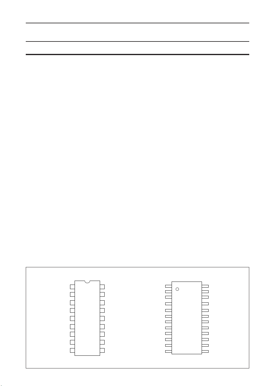
• 18-pin plastic DIP(DIP18-P-300)
• 24-pin plastic SOP
PIN CONFIGURATION
MSM62X42BRS
(TOP View) 18 Lead Plastic DIP
1
STD.P
2
CS
0
ALE
3
4
A
0
5
A
1
6
A
2
A
7
3
8
RD D
910
GND
Note: The actual type name indicates the abbreviated one, M62X42B.
MSM62X42BGS-1K
(TOP View) 24 Lead Plastic SOP
1
18
V
DD
17
(VDD)
16
)
(V
DD
15
CS
1
14
D
0
13
D
1
D
12
2
11
3
WR
STD.P
2
CS
0
3
NC
4
ALE
5
A0
6
NC
7
A
1
8
NC
9
A
2
10
A
3
11
RD
12
GND WR
NC : NO CONNECTION (unused pins)
24
V
DD
(VDD)
23
(V
)
DD
22
21
NC
20
CS
1
19
0
D
18
NC
17
NC
16
D
1
15
D
2
14
D
3
13
41
Page 2
RANK
¡ SemiconductorMSM62X42B
M62X42B
JAPAN xxxxA
Lot no. Stability A or B
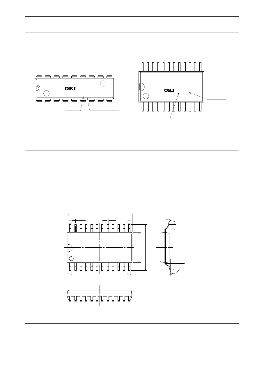
EXTERNAL DIMENSION
1.27 0.35
24 13
A: 10PPM
B: 50PPM
16.3 MAX
M62X42B
xxxxS
Stability S or B
±
S: 20PPM
±
B: 50PPM
±
±
Lot no.
(UNIT : mm)
0.2
1.0
42
8.0MAX
12.2MAX
0.3MAX
10
2.58
~
0
1
12
MAX
Page 3
¡ Semiconductor MSM62X42B
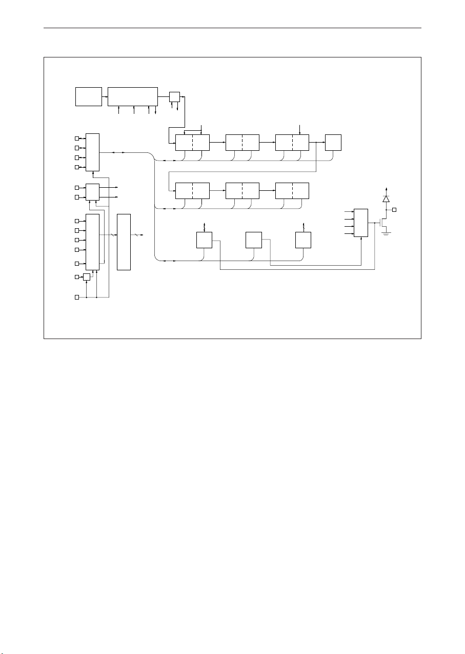
FUNCTION BLOCK DIAGRAM
CS
ALE
CS
D
D
D
D
WR
RD
A
A
A
A
3
2
1
0
3
2
1
0
32.768kHz
0
1
X'tal
OSC
&
T
E
COUNTER
RESET
STOP
bit
bit
G
A
T
E
G
A
G
A
T
E
&
L
A
T
C
H
D
E
C
O
D
E
R
1Hz
30 sec ADJ
bit
S
1
~
C
F
HOLD
bit
BUSY
bit
30 sec ADJ bit
S
1S10
D
1D10
MI1MI
10
MO1MO
10
C
D
C
E
* S1 ~ W ~ Y10 are time counter register.
~ CF are control register.
* C
D
24/12 bit
H1H
Y1Y
10
10
C
F
W
64Hz
1 sec carry
1 min carry
1 hour carry
V
DD
STD.P
43
Page 4

REGISTER TABLE
¡ SemiconductorMSM62X42B
Address
Input
0
1
2
3
4
5
6
7
8
9
A
B
C
D
S
SI
mi
mi
h
PM/
AM
d
*
mo
*
y
y
w
2
4
40
40
4
4
4
40
4
Data
4
4
D
S
S
mi
mi
h
d
mo
y
w
Count
value
D
1
0
0 to 9
S
2
1
0 to 5
S
20
10
0 to 9
mi
2
1
0 to 5
mi
20
10
h
d
mo
MO
0 to 9
h
1
0 to 2
10
or 0 to 1
0 to 9
d
1
0 to 3
10
0 to 9
1
0 to 1
10
0 to 9
y
1
0 to 9
y
10
0 to 6
w
1
h
2
20
d
2
20
2
*
y
2
20
2
Description
1-second digit register
10-second digit register
1-minute digit register
10-minute digit register
1-hour digit register
PM/AM,
10-hour digit register
1-day digit register
10-day digit register
1-month digit register
10-month digit register
1-year digit register
10-year digit register
Week register
A
A
A
3
2
0
0
0
0
0
0
0
0
0
1
0
1
0
1
0
1
r
0
1
0
1
0
1
0
1
1
Register
A
1
0
Name
0
0
S
0
1
S
1
0
MI
1
1
MI
0
0
0
1
H
1
0
D
1
1
D
0
0
MO
0
1
MO
1
0
Y
1
1
Y
0
0
D
3
S
1
10
10
H
i
10
1
10
1
10
W
8
*
mi
1
8
*
h
8
*
d
8
*
mo
1
10
8
*
y
8
y
80
*
D
1
1
0
1
E
1
1
1
0
F
1
1
1
1
0 = "L" level, 1 = "H" level
REST = RESET
PM/AM = 1/0
ITRPT/STND = INTERRUPT/STANDARD
Notes:
1) The writing of bit * is at discretion, but it is handled as "0" in the internal. In addition, it is
unconditionally held at "0" during a read.
2) The writings of "1" to IRQ FLAG bit, and "0" and "1" to BUSY bit are at discretion, but they are not
carried out. The reading can be done. The writing of "0" to the IRQ FLAG bit is carried out.
3) The bits except bit * and the BUSY bit can fully be read and written. However, the writing to the IRQ
FLAG is effective for "0" only.
4) PM/AM bit is 1 at PM and 0 at AM.
44
30 sec.
C
D
C
E
C
F
ADJ
t
1
TEST
IRQ
FLAG
t
0
24/12
BUSY
ITRPT
/STND
STOP
HOLD
MASK
REST
—
—
—
r
r
r
Page 5
¡ Semiconductor MSM62X42B
ELECTRICAL CHARACTERISTICS
Absolute Maximum Ratings
Parameter Symbol Conditions Rating Unit
Power supply voltage
Input voltage V
I
Output voltage Vo
Storage temperature
Soldering conditions (lead)
Operating Conditions
Parameter Symbol Conditions Rating Unit
Power supply voltage
Time Recording Supply Voltage
Crystal Frequency
Operating Temperature
Note:
Time Recording Supply Voltage: Power supply voltage to guarantee a crystal oscillator and time recording
Frequency Accuracy
Item Conditions Rating Unit
V
DD
Ta = 25°
T
STG
T
SOL
V
DD
V
CLK
f
(XT)
T
OP
—
—
—
—
—
—
– 0.3 to 7
-03 to VDD +0.3
-03 to VDD +0.3
–55 to +85
Temp.:under 260°C
Time :within 10 seconds
4.5 to 5.5
2.0 to 5.5
32.768
–40 to +85
V
V
V
°C
V
V
kHz
°C
Frequency stability
Temperature Characteristics
OCS starting time
Frequency Drift
Voltage characteristics
Rank A : 18pin DIP only
*
Rank S : 24pin SOP only
Rank B : 18pin DIP, 24pin SOP
Rank A
Rank S
Rank B
Ta = 25°C
VDD = 5V
–10 to +70°C (25°C standard)
–40 to +85°C (
´´
At 4.5V, let "t" make "0"
Ta=25°C, V
DD
= 5V
First year
Ta=25°C
V
= 4.5~5.5V
DD
± 10
± 20
PPM
± 50
+10/ –120
)
+10/ –220
MAX 1
± 5
± 5
PPM
Sec.
PPM/year
PPM/V
45
Page 6

D.C. Characteristics
(V
DD
Parameter Symbol Conditions Applicable TerminalUnit
Min.
Typ.
¡ SemiconductorMSM62X42B
= 5V ± 10%, Ta = –40 to +85°C)
ax
"H" Input voltage (1)
"L" Input voltage (1)
Input leak current (1)
Input leak current (2)
"L" output voltage (1)
"H" output voltage
"L" output voltage (2)
OFF leak current
Input capacitance (1)
Input capacitance (2)
Current
consumption (1)
Current
consumption (2)
"H" input voltage (2)
"L" input voltage (2)
V
IH1
V
IL1
I
LK1
I
LK2
V
OL1
V
OH
V
OL2
I
OFFLK
C11
C12
I
DD1
I
DD2
V
1H2
V
1L2
V1 = VDD/0V
IOL = 2.5mA
IOH = 400µ A
IOL = 2.5mA
VI = VDD/0V
Input frequency 1MHz
f(xt) =
32.768
V
DD
= 5V
kHz
~
CS1
~
V
=2~5.5V
DD
DD
= 2V
0V
V
4/5V
2.2
—
—
—
—
2.4
—
—
—
—
—
—
—
—
—
—
0.8
—
1/–1
—
10/–10
—
0.4
—
—
—
0.4
All input terminals
V
except CS
Input terminals other
than D0 ~D
µA
D0 ~ D
V
D0 ~ D
V
1
3
3
3
STD. P
—
10
µA
5
—
5
—
—
30
—
1.8
—
DD
—
—
1/5V
DD
Input terminals other
than D
PF
D0 ~D
V
µA
DD
CS1
V
3
to D
0
3
46
Page 7
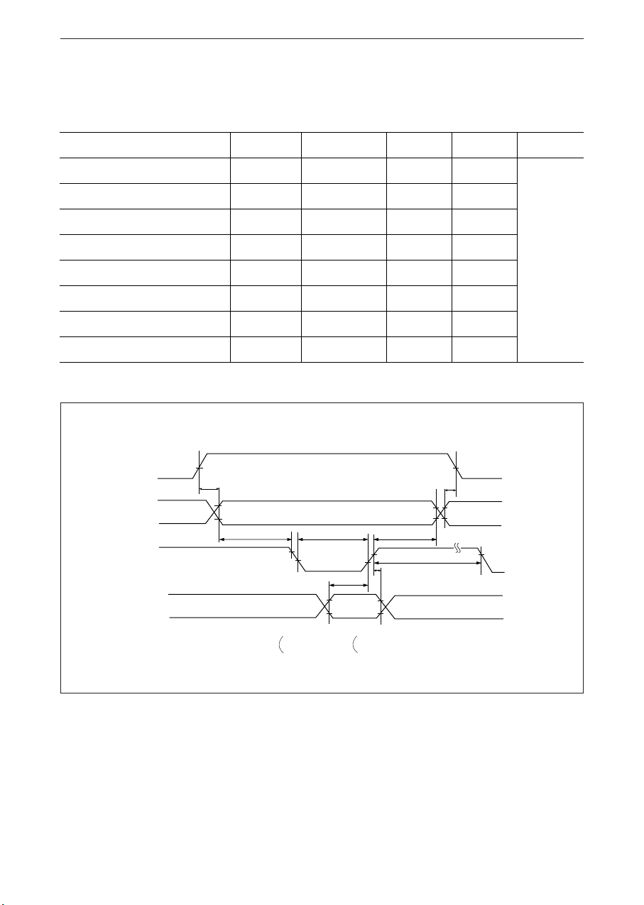
¡ Semiconductor MSM62X42B
Switching Characteristics
WRITE mode (ALE = VDD)
(V
= 5V ± 10%, Ta = –40 to +85°C)
DD
Parameter Symbol Conditions Min. Unit
Max.
CS1 Set up Time
CS1 Hold Time
Address Stable Before WRITE
Address Stable After WRITE
WRITE Pulse Width
Data Set up Time
Data Hold Time
RD/WR Recovery Time
CS
1
A0~A
3
CS
0
WR
D0~D
3
(INPUT)
t
C1S
t
C1H
t
AW
t
WA
—
—
—
—
1000
1000
20
10
—
—
—
—
ns
t
WW
t
DS
t
DH
t
RCV
V
IH2
t
C1S
V
IH1
V
IL1
t
Aw
V
IH1
—
—
—
—
t
ww
V
V
IL1
t
DS
V
IH1VIH1
V
IL1VIL1
IL1
120
100
10
60
t
wA
V
IH1
t
RCV
t
DH
—
—
—
—
V
IH2
t
C1H
V
IH1
V
IL1
V
IH1
V
V
IH1
IL1
= 2.2V
= 0.8V
V
=
4
/5
V
IH2
V
DD
1
/5
V
=
DD
IL2
47
Page 8
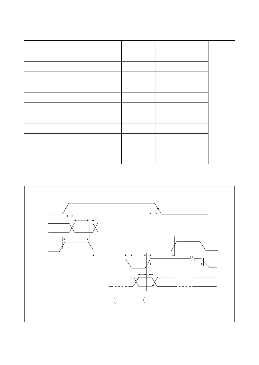
WRITE mode (with use of ALE)
Parameter Symbol Conditions Min. Unit
¡ SemiconductorMSM62X42B
(V
= 5V ± 10%, Ta = –40 to +80°C)
DD
Max.
CS1 Set up Time
Address Set up Time
Address Hold Time
ALE Pulse Width
ALE Before WRITE
WRITE Pulse Width
ALE After WRITE
Data Set up Time
Data Hold Time
CS1 Hold Time
RD/WR Recovery Time
CS
1
A0~A
3
CS
0
ALE
WR
D
0~D3
(Input)
t
C1S
t
AS
t
AH
t
AW
t
ALW
t
WW
t
WAL
t
DS
t
DH
t
C1H
t
RCV
V
IH2
t
C1S
t
t
AS
AH
V
IH1
V
IL1
t AW
V
V
IH1
V
IH1
V
IL1
IH1
V
IL1
t
ALW
V
—
—
—
—
—
—
—
—
—
—
—
t
WW
IH1
V
IL1
t
DS
V
IH1
V
IL1
1000
25
25
40
10
120
20
100
10
1000
60
V
IH2
t
C1H
t
WAL
V
IH1
V
IL1
t
t
RCV
DH
V
IH1
V
IL1
—
—
—
—
—
—
ns
—
—
—
—
—
V
IH1
48
V
V
IH1
IL1
= 2.2V
= 0.8V
V
=
4
/5
V
IH2
V
IL2
DD
1
/5
V
=
DD
Page 9
¡ Semiconductor MSM62X42B
READ mode (ALE = VDD)
(V
= 5V ± 10%, Ta = –40 to +85°C)
DD
Parameter Symbol Conditions Min. Unit
Max.
CS1 Set up Time
CS1 Hold Time
Address Stable Before READ
Address Stable After READ
RD to Data
Data Hold
RD/WR Recovery Time
CS
1
A0~A
3
CS
0
RD
D0~D
3
(Output)
t
C1S
t
C1H
t
AR
t
RA
t
RD
t
DR
t
RCV
V
IH2
t
C1S
t
AR
V
IH1
V
IL1
V
IH1
V
t
IL1
RD
—
—
—
—
CL = 150 pF
—
—
V
IL1
V
OH
V
OH
V
V
OL
OL
1000
1000
20
0
—
0
60
t
C1H
t
RA
V
IH1
t
RCV
t
DR
—
—
—
ns
120
—
—
V
IH2
V
IH1
" Z "
V
V
IH1
IL1
= 2.2V
= 0.8V
V
=
4
/5
V
IH2
1
/5
V
=
V
IL2
VOH = 2.2V
DD
DD
V
= 0.8V
OL
49
Page 10

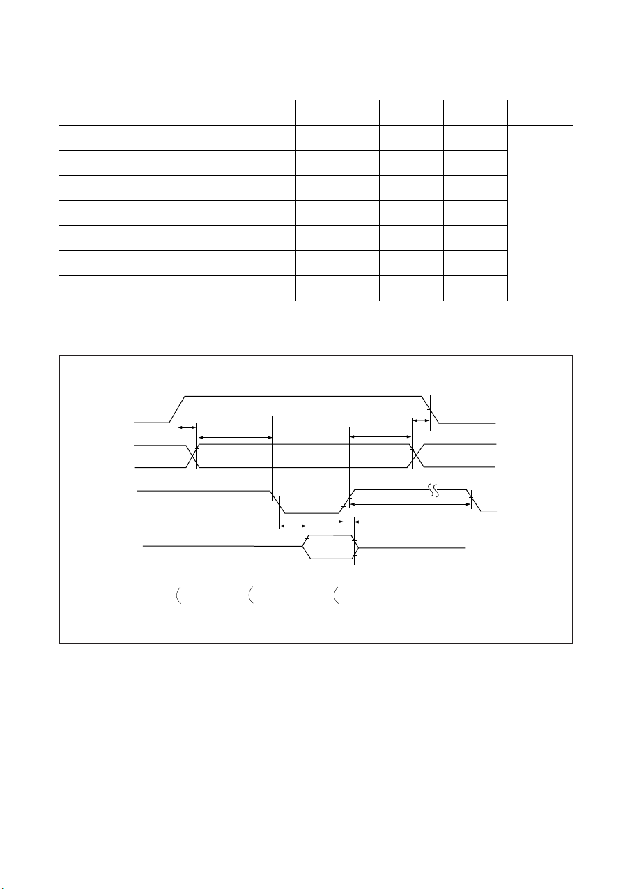
READ mode (with use of ALE)
Parameter Symbol Conditions Min. Unit
¡ SemiconductorMSM62X42B
(V
= 5V ± 10%, Ta = –40 to +85°C)
DD
Max.
CS1 Set up Time
Address Set up Time
Address Hold Time
ALE Pulse Width
ALE Before READ
ALE After READ
RD to Data
DATA Hold
CS1 Hold Time
RD/WR Recovery Time
CS
1
A0~A
3
CS
0
ALE
RD
D
0~D3
(Output)
t
C1S
t
AS
t
AH
t
AW
t
ALR
—
—
—
—
—
1000
25
25
40
10
—
—
—
—
—
ns
t
RAL
t
RD
t
DR
t
C1H
t
RCV
V
IH2
t
C1S
t AS
V
IH1
V
IL1
t
AW
V
IH1
V
IH1
t
AH
V
IH1
V
IL1
V
IL1
t
ALR
—
CL = 150pF
—
—
—
V
IH1
t
DR
10
–
0
1000
60
V
IH2
t
C1H
t
RAL
V
V
IH1
IL1
V
IL1
t
DR
V
OH
V
OL
—
120
—
—
—
V
IL1
V
t
RCV
" Z "
IH1
50
V
V
IH1
IL1
= 2.2V
= 0.8V
V
=
4
/5
V
IH2
1
/5
V
=
V
IL2
VOH = 2.2V
DD
DD
V
OL
= 0.8V
Page 11

¡ Semiconductor MSM62X42B
PIN DESCRIPTION
D0 to D3 (Data buses 0 to 3)
Data input/output pins to be directly connected to a microcomputer data bus for reading
and writing of the register controlled by the microcomputer. The interface serves as positive
logic and CS0=L, 1=H, RD=L, and as output mode when WR=H. It becomes high impedance
except these cases.
A0 to A3 (Address buses 0 to 3)
These are input pins to be directly connected to a microcomputer address bus for register
assignment which is read and written by a microcomputer. These address data are used in
combination with ALE for addressing registers.
ALE (Address Latch Enable)
This is an input pin to read address data and CS0.
The address bus andCS0 are read into a IC when ALE="H". The address data in the case of
ALE=L in the IC is held. CS1 functions to ALE independently.
When the microcomputer of MSC-48, 51 or 80 system having an ALE output is used, this pin
is connected to the ALE output of the microcomputer. When 4 Bits of A0 to A3 in a 4 Bit
microcomputer are commonly used with an another peripheral IC. When the microcomputer does not have the ALE output, the ALE input of this IC is fixed to "H".
WR (WRITE)
This is a input pin for which the data is written into this IC by a microcomputer. When
CS1=H, D0 ~ D3 data are written into the designated registers by A0 to A3 and ALE at the
rising edge of WR.
RD (READ)
This is an input pin to read this IC data by a microcomputer. When CS1=H, RD outputs the
register data designated by A0 to A3 and ALE during "L". If both WR and RD are set at "L",
this should be inhibited because it becomes the cause for malfunction.
CS0, CS1(Chip Select
0•1
)
These pins enable/disable ALE, RD and WR operation, when CS1=H at CS0=L, these pins
become effective. In other combination except this, the pins become equivalent to ALE=L
and WR=RD=H unconditionally in the IC internal. However, CS0 needs operation related
with ALE, while CS1 works independently to ALE. CS1 must be connected to the power
supply voltage detector. Refer to the item, “CS1 of APPLICATION NOTE”.
STD • P (STANDRD Pulse)
Output pin of N-CH OPEN DRAIN type. The output data is controlled by the D1 data
content of CE register. This pin has a priority to CS0 and CS1. Refer to the item "CE REGISTER
FOR FUNCTIONAL DESCRIPTION OF REGISTERS".
V
DD
STD.P Output
N-CH
51
Page 12

¡ SemiconductorMSM62X42B
(VDD)
Both pins are shorted to VDD. They should be left open or connected to 18 pin (DIP) or 24
pin (SOP).
VDD • V
SS
These are a positive power supply pin VDD and a ground pin VSS.
FUNCTIONAL DESCRIPTION OF REGISTERS
Register names: S1, S10, MI1, MI10, H1, H10, D1, D10, MO1, MO10, Y1 Y10, W
a) These are abbreviations for Second1, Second10, MI nute1, MI nute10, Day1, Day10, Month1,
Month10, Year1, Year10 and week. These values are in BCD notation.
b) Refer to the Register table for details. All registers are logically positive. For example, (S8,
S4, S2, S1) = 1001 which means 9 seconds. In addition, the * mark in the rgister table is good
for either case of "1" or "0" in the case of writing and becomes “0” automatically in the case
of reading.
c) If data is written which is out of the clock register data limits, it can result in erroneous clock
data being read back. Therefore, avoid to set not existing data.
d) PM/AM h20, h
In 12-hour mode, the time of AM12 ~ AM11 and PM12~ PM11 exists. In 24-hour mode, the
time exists from 0 hour to 23 hour.
In the mode setting of 24-hour mode, PM/AM bit is ignored, while in the mode setting of 12hour mode, h20 is to be set. Otherwise it causes discrepancy.
In reading out the PM/AM bit in the 24-hour mode, it is continuously read out as 0. In
reading out h20 bit in the 12-hour mode, 0 is written into this bit first, then it is continuously
read out as 0 unless 1 is being written into this bit.
10
e) Registers Y1, Y10 and Leap Year
This IC is designed exclusively for the Christian Era and is capable of identifying a leap year
automatically.
80, 84 88 ------- leap years
When a non-existant day of the month less than 31 day is set, for example, if the data February
29, or November 31, 1983 was written, it would be changed automatically to March 1 or
December 1, 1983 at the exact time at which a carry pulse occurs for the day's digit.
52
Page 13

¡ Semiconductor MSM62X42B
f) Regarding W
The Register W data limits are up-counted from 0 to 6. The following Table 1 shows a possible
data definition.
TABLE 1
W4
W2
W1
Day of Week
0
0
0
0
1
1
1
0
0
1
1
0
0
1
0
1
0
1
0
1
0
Sunday
Monday
Tuesday
Wednesday
Thursday
Friday
Saturday
CD REGISTER (Control D Register)
a) HOLD (D0)
• This Register is one means used for reading out registers S1 to W (addresses 0 to C) and
a bit used for writing. "1" bit to this bit is written and when BUSY bit shows "0", the clock
more than 1 second digit stops and the reading and writing become possible (Refer to the
item APPLICATION NOTE for reading which does not use HOLD bit). When BUSY was
"1" and after reading have finished, "0" is written to HOLD bit. If the writing of "0" is
omitted, then this results in the cause for erroneous data. Setting this bit to "1" inhibits
a carry to 1 second counter in the IC internal, but a carry to a second counter caused during
the duration of "1" is automatically compensated (+1 second) by only one time at the time
when "0" is written to this bit. However, the carry after the second is disregarded and is
not compensated (loss second).
• If CS1 makes "L", the HOLD bit becomes equivalent to the writing to "0" and becomes "0".
b) BUSY (D1)
• The status bit in the IC internal which shows the interface condition with a microcomputer. When the registers S1 to W (addresses 0 to C) is written, when HOLD bit is always
"1" and when BUSY bit is surely "0", in case the HOLD bit is used for reading, this is
performed when the BUSY bit is "0". "0" of the BUSY bit continues while the HOLD bit
is "1". When the HOLD bit makes "0", the BUSY bit becomes "1".
• The operation for the registers CD, CE and CF is irrespectively performed for the HOLD
bit and BUSY bit.
• The BUSY bit is "1" uncondiotinally when the HOLD bit=0 and when "1" written into the
HOLD bit, BUSY or not BUSY can be confirmed and when BUSY="1", "0" is once written
into the HOLD bit, and then "1" is again written. BUSY is checked. The routine procedure
like this [HOLD ¨ "0", HOLD ¨ "1", BUSY check] is repeated, or after "0" is written into
the HOLD bit, "1" is again written into the HOLD bit after 190µs and BUSY=0 is
confirmed.
• The time when this IC is BUSY is 190µs per one second
• The writing into the BUSY bit cannot be performed.
53
Page 14

¡ SemiconductorMSM62X42B
c) IRQ FLAG (D2) (Interrupt Request FLAG)
This status bit corresponds to "L" or "OPEN" of the STD.P output pin. When STD.P="L", then
this bit=1 and when STD.P=OPEN, then this bit=0.
This bit indicates that an interrupt has occurred to a microcomputer mainly. When D0 of
register CE(MASK)=0, then the STD.P output changes from OPEN to "L" and this bit changes
from "0" to "1" according to the timing set by D3(t1) and D2(t0) of the register CE.
When D1(ITRPT/STND) of the register CE is 1 (interrupt mode), the "1" of this bit (the "L" of
the STD.P output) remains until "0" is written into this bit. When this bit is "1" and timing
for a new interrupt occurs, the new interrupt is ignored. When D1(ITRPT/STND)=0 (fixed
cycle output waveform mode), the "1" of this bit (the "L" of the STD.P output) keeps "1" until
either "0" is written to this bit, or this bit automatically returns after 7.8125ms. The using
examples for the alarm are shown in the item "Set STD.P at alarm mode of APPLICATION
NOTE".
d) 30 sec. ADJ bit (30 sec. ADJUST)
This is a bit for 30-second adjustment. When "1" is written into this bit, the compensation for
30 seconds is performed. The duration for 125µs from the time written into this bit should
not be read from or written into registeres S1 ~ W (addresses 0 ~ C).
This bit for 125µs from the time written into this bit is kept in "1" and then it will automatically
return to "0". After "1" is written into this bit, the registeres S0 ~ W (addresses 0 ~ C) are
operationed with confirmation of automatical return to "0" of this bit.
CE REGISTER (Control E Register)
a) MASK (D0)
This bit controls the STD.P output. When this bit=1, then the STD.P output becomes open.
When this bit=0, then the STD.P output=output mode. The relationship between the MASK
bit and STD.P output is shown as follows.
• In the case of interrupt mode (ITRPT/STND bit="1")
• In the case of fixed cycle output waveform mode (ITRPT/STND bit="0")
54
MASK BIT
STD.P OUTPUT
IN TRT/STND BIT = "1"
"1" "1"
"0""0"
WRITE “0” INTO IRQ FLAG BIT
"INTERRUPT" DOES
NOT OCCUR BECAUSE
MASK BIT IS "1"
OPEN
LOW LEVEL
"INTERRUPT" TIMING
Page 15

¡ Semiconductor MSM62X42B
OUTPUT DOES NOT OCCUR
"1"
AT LOW LEVEL BECAUSE
MASK BIT IS "1"
OPEN
LOW LEVEL
OUTPUT TIMING
AUTOMATIC RETURN
(When “0” is written to IRQ FLAG bit, at that time, STD.P
output becomes open without awaiting automatic return.)
MASK BIT
STD.P
OUTPUT
IN TRT/STND BIT = "0"
"1"
"0""0"
b) ITRPT/STND (D1) (INTERRUPT/STANDARD PULSE)
This is a bit which gives the meaning for STD.P output. When this bit="1", the request for
interrupt is outputted at the STD.P output and when this bit="0", a fixed cycle waveform with
a low-level pulse width of 7.8125ms is present at the STD.P output. However, at this time,
the MASK bit must equal 0, while the period in either modes is determined by t0 (D2) and
t1(D3) of register CE.
c) t0 (D2), t1 (D2) (time 0, 1)
• When ITRPT/STND bit="1", this bit determines the interrupt period. When ITRPT/
STND bit="0", this bit determines the period of fixed timing waveform. The periods are
shown in the table below.
t
t
1
0
Period
Duty CYCLE of "L" level when
INRPT/STND bit is "0".
0
0
0
1
1
0
1
1
1/64 second
1 second
1 minute
1 hour
1/2
1/128
1/7680
1/460800
• The timing of the STD.P output designated by t1 and t2 occurs at the moment that a carry
occurs to a clock digit.
(EXAMPLE) WHEN t1 = 1, t0 = 1 and MASK = 0
PM12:00 PM1:00
WHEN ITRPT/STND
BIT is "1"
STD.P OUTPUT
WHEN ITRPT/STND
BIT is "0"
OPEN
LOW LEVEL
OPEN
LOW LEVEL
The special counter is not included for t1 and t0.
55
Page 16

¡ SemiconductorMSM62X42B
• The low-level pulse width of the fixed cycle waveform is 7.8125ms independent of t0/t
inputs.
• The fixed cycle output waveform mode is available for the confirmation of the crystal
oscilltor frequency.
• During ±30 second adjustment a carry can occur that will cause the STD.P output to go
"L" when t0/t1=1,0 or 1,1. However, when ITRPT/STND bit=0, the "L" is kept from
clearing under the second of 30-second ADJ to resuming a carry to 1/64-second digit.
• No STD.P output change occurs as a result of writing data to registers S1 ~ H1.
CF REGISTER (control F Register)
a) REST (D0) (RESET)
This bit is used to reset the clock's internal counter of less than a second. When RTEST=1, the
counter is Reset for the duration of REST. In order to release this counter from Reset, a "0"
must be written to the REST bit. If CS1=0, then REST=0 automatically.
b) STOP (D1) (STOP)
This bit is used for the integrating clock. When "1" is written, the timing after 8,192Hz stops
and swhen "0" is written, the timing starts again.
"1"
STOP BIT
TIMING OF
"CARRY"
TO 8192Hz
"1"
"0""0" "0" "0"
"1"
"CARRY" EXECUTED
1
"CARRY" NOT EXECUTED
c) 24/12 (D2) (24 Hour/12 Hour)
• This bit is for selection of 24/12 hour time modes, if D2=1, 24 hour mode is selected and
the PM/AM bit is invalid. If D2=0,12 hour mode is selected and the PM/AM bit is valid.
• The writing into the 24/12 hour bit is performed only when RESET bit=1. [24/12 hour
bit=*1 and RESET bit="1"] must be written and then [24/12 hour bit=*2 and RESET
bit="0"] must be written continuously. However, in the case of *1=*2 and *1≠*2, the 24/
12 hour bit becomes indefinite.
• When 24/12 hour bit is rewritten, the data of more than H1 may be destroyed. Therefore,
the data of more than H1 must be newly rewritten.
• When REST bit=0, the 24/12 hour bit cannot be written.
d) TEST (D3)
• This is a bit for the test. This bit is used in the state of TEST bit=0.
• When TEST bit is "1", because of the test function based on our company's convenience,
the user's function is not guaranteed.
56
Page 17

¡ Semiconductor MSM62X42B
APPLICATION NOTE
Power Supply
Start
V
= 0 to VDD= 5V
DD
Power On
TEST bit
REST bit
24/12 bit
STOP bit
REST bit
24/12 bit
Set the current Time
HOLD bit
STOP bit
¨
¨
¨
*1
¨
¨
¨
¨
0
1
1
0*2¨
0
0
All registers and STD,P
output=undefined
*1=*2(=1 or 0)
Start Operation
Pattern Layout
The oscillation circuit of 32.768kHz consists of high impedance in the oscillation stage to
realize the minimum current consumption. In addition, it is a feature that the time when the
oscillation waveform passes the threshold vicinity is long. For this reason, the power supply
anti-noise by the same method as an analog IC must be considered. As an actual example,
set a tantalum capacitor (4.7µF) and a ceramic capacitor (0.01µF) near this IC. In case that an
another IC, for instance, RAM for backup, exists in battery backup circuit, set a bypass
capacitor close to it.
Maximum value of allowable power supply noise should be 300mV.
57
Page 18

¡ SemiconductorMSM62X42B
Reading and Writing of Registers S1 ~ W and Writing of 30-Second ADJ Bit
Registers S1 ~ W (Addresses 0 ~ C)
Reading and writing in the case of using HOLD bit
HOLD bit ¨ 1
READ BUSY bit
BUSY bit = 0 ?
YES
Write data into or
Read data from
registers S1~W
HOLD bit ¨ 0
In the inside of LSI, the CLEAR of BUSY bit is performed when
*
HOLD bit = 0, but, if the period of HOLD bit =0 is extermely
narrow as compared with the period of HOLD bit = 1, there is
some case that the CLEAR of BUSY bit delays so that the
BUSY bit can be cleared by sampling HOLD bit = 0 at approximate
16KHz. It is recommended to allow an idling time of 62ms or more.
NO
HOLD bit ¨ 0
Idling time
*
58
Page 19

¡ Semiconductor MSM62X42B
Reading method 1 in the case of not using HOLD bit
Reading from
Registers S1~W
DATA1 ¨
Reading from
Registers S1~W
DATA2 ¨
DATA1=DATA2
END
Data of
Registers
S1~ W
Data of
Registers
S1~ W
YES
First
Second
NO
The reason why the registers are read
*
twice is to avoid the case during the
variation of information because a
carry has occurred accidentlly.
Reading method 2 in the case of not using HOLD bit
*1
←
t
1
←
t
0
ITRPT/STND ←
MASK ←
*2
1
0
Initial setting only at power On
• *1 and *2 represent the minimum required time unit.
For example
t
=0 and t0=1 when required to a unit of second
1
t
=1 and t0=0 when required to a unit of minute
1
t
=1 and t0=1 when required to a unit of hour
1
Note
IRQ FLAG ← 0
WAIT t
TIME DATA READ
See Note below
REGISTER CD READ
IRQ FLAG=0
YES
Normal read
t : 12 hour mode 35µs
24 hour mode 3µs
~
Retried the reading since a carry occurred during the operation.
(Note)
NO
Do this process within the following time requirements
by combination between t
t1=0, t0=1 within 1 second
t
=1, t0=0 within 1 minute
1
t
=1, t0=1 within 1 hour
1
1
and t
.
0
59
Page 20

(B)
Reading mehtod 3 in the cass of not using HOLD bit
¡ SemiconductorMSM62X42B
END
YES
*1
*2
1
0
CPU senses the
interruption.
NO
¨
t
1
¨
t
0
ITRPT/STND ¨
MASK ¨
REGISTER CD READ
IRQ FLAG=1
WAIT t
TIME DATA READ
IRQ FLAG ¨ 0
Writing 30-Second ADJ bit (Two Ways A, B)
START
• Initial setting only in power On
• *1 and *2 represent the minimum required time unit.
For example
t
=0 and t0 =1 when required to a unit of second
1
=1 and t0 = 0 when required to a unit of minute
t
1
t
=1 and t0 =1 when required to a unit of hour
1
The other IC causes the interruption.
The interruption is caused by this IC due to
the occurrence of a carry
t : 12 hour mode 35µs
24 hour mode 3µs
The IRQ FLAG is cleared to read the next
time data.
60
30-SECOND ADJ BIT ¨ 1
READ 30-SECOND ADJ BIT
30-SECOND ADJ BIT=0?
YES
END
(A)
START
30-SECOND ADJ BIT ¨ 1
120µs PASS ?
YES
END
NO
NO
•
The reading from or writing into all
bits of registers C
out without any relation to HOLD
bit.
and CP can carry
D
Page 21

¡ Semiconductor MSM62X42B
CS1 (Chip Select)
VIH and VIL of CS1 have 3 functions:
1. To accomplish the interface with a microcomputer in 5V operation.
2. To inhibit the control bus, data bus and address bus and to reduce input gate pass current
in the stand-by mode.
3. To protect internal data when the mode is moved to and from stand-by mode.
To realize the above functions:
1. More than 4/5 VDD should be applied to this IC for the interface with a microcomputer in
5V operation.
2. In moving to the stand-by mode, 1/5 VDD should be applied so that all data buses should
be disabled. In the stand-by mode, approx. 0V should be applied.
3. To and from the stand-by mode, obey the following Timing chart.
] The stand-by mode means the power supply voltages from 4V to 2V up to the minimum
value (2V) of the operating power supply voltage and the interface with the IC external is not
guaranteed while the clock time works.
To Standby Mode From Standby Mode
V
DD
CS
1
The CS
0
2
V
DD
5
of this IC does not
generate "H" or WR during
4V
2µs (MIN)
4~6V
2~4V
Less than
4V
1
V
DD
5
The interface with this IC
is available after this.
2µs (MIN)
4
V
DD
5
this duration.
As a matter of fact, regard this matter as the
data holding in the stand-by of STATIC RAM.
61
Page 22

Set STD.P at alarm mode
Set alarm at 9:00
¡ SemiconductorMSM62X42B
MASK BIT
ITRPT/STND BIT
t1 , t0
Read Register R
D2 =1 ?
YES
Read H
10 and
H1 Content
AM 9:00?
YES
¨
0
¨
1
¨
1, 1
Start interruption
CPU Activation
D
NO
NO
CPU HALT
CPU STAND BY
Repeat
or
62
Page 23

¡ Semiconductor MSM62X42B
TYPICAL APPLICATION - POWER SUPPLY CIRCUIT
(A capacitor for bypass should be attached near the IC.)
[When supplied from +5V power supply system.]
4.7µF
Tantalum capacitor
0.01µ
Ceramic
capacitor
V
DD
GND
MSM62X42B
51K
10K
+5.1V
10K
A495
100
C372
(sat) = 0.1v
V
CE
W
+
22µ
++
When the power is changed from ON to OFF, the
reverse-current flows temporally from collector to
emitter of a transistor. Therefore, use a capacitor
of large capacitance here.
W
100
0.01
4.7µF
+
Tantalum
capacitor
µF
Ceramic
capacitor
V
DD
GND
+ 5 V
1.2V ¥ 3 = 3.6V
Ni–Cd batteries
RL
M
RL
B
C
+
1.5¥2=3V
Dry cells
–
[When supplied from higher power supply system than +5V.]
+ V (Higher power
supply over about 1.5V than +5V)
+5V
(Power supply
of peripheral circuit)
R1
D1
(Ni–Cd batteries)
3.6V
R2
+5.7V
D2
100
+
–
4.7µ
W
+
Tantalum
capacitor
MSM62X42B
0.01µ
Ceramic
capacitor
V
DD
GND
MSM62X42B
(Note) In order to reduce the level difference to VDD between +5V and MSM62 x 42B, use the
same diodes for D1 and D2.
63
Page 24

¡ SemiconductorMSM62X42B
IS1588
= 0.69V
V
F
+5.7V
C372
V
= 0.69V
F
or
100 W
+
–
4.7µF
+
Tantalum
capacitor
0.01µ
Ceramic
capacitor
V
DD
GND
MSM62X42BRS
1.2 ¥ 3 = 3.6V
Ni–Cd batteries
TYPICAL APPLICATION INTERFACE WITH MSM62X42B AND MICROCOMPUTER
(8085)
8085
A4~A
IO/M
AD
AD
AD
AD
ALE
RD
WR
MSM62X42B
3
2
1
0
15
S
1
S
2
DECODER
D
3
D
2
D
1
D
0
A
3
A
2
A
1
A
0
CS
0
ALE
R
1
RD
R
2
WR
or
8085
AD0~AD
A0~A
A12~A
IO/M
RD
WR
11
15
S
S0
3
1
MSM62X42B
DECODER
R
1
R
2
D
D
D
D
A
A
A
A
CS
ALE
RD
WR
3
2
1
0
3
2
1
0
0
Note 1) If the address of program memory and the address of MSM62X42B do not overlap, the
S1 and S0 of the Decoder are not required.
Note 2) If the address of IO/MSM62X42B for the decoder does not overlap with other
addresses, this is not required.
Note 3) If 8085 does not enter into the state of HALT or HOLD during CS1 = "H" of MSM62X42B,
R1 and R2 are not required.
64
Page 25

¡ Semiconductor MSM62X42B
(Z80)
Z80
A0~A
or
MREQ
(MCS48)
MCS48
BUS
BUS
BUS
BUS
BUS
D
D
D
D
A
A
A
A
IORQ
RD
WR
4~7
MSM62X42B
3
2
1
0
3
2
1
0
DECODER
15
G
1
G
2
D
3
D
2
D
1
D
0
A
3
A
2
A
1
A
0
CS
0
V
DD
ALE
Note) It depends upon the switch-
ing characteristics decided by
a X’tal used for a Z80 that
either of IORQ and MREQ is
used.
RD
WR
MSM62X42B
D
3
2
1
0
DECODER
D
D
D
CS
3
2
1
0
A
3
A
2
A
1
A
0
0
ALE
RD
WR
ALE
RD
WR
65
Page 26

REFERENCE DATA
(1) Frequency vs. Temperature
¡ SemiconductorMSM62X42B
Temp. (°C)
–20 –10 0 10 20 30 40 50 60 70
0
–10
–20
–30
–40
–50
–60
Frequency Df/f (ppm)
–70
Typical
qT = 25°C
a = –0.035ppm/°C2
(2) Current Consumption vs. Supply Voltage
I
DD
[µA]
CS1 = 0V
30
at 25°C
25
20
15
10
5
2.0 3.0 4.0 5.0 [V]
Frequency temperature characteristics can be
estimated as follows:
Dfx (PPM) = f0T + a(qT – qx)
2
Dfx (PPM) : frequency shift at arbitrary
: temperature
f0T (PPM) : frequency shift at qT
a(PPM) : temperature coefficient
: (–0.035 ppm/°C2 ± 0.005
: (ppm/°C
2
)
qT (°C) : turning point temperature
: (25°C ± 5°C)
qx (°C) : arbitrary temperature
11.574 ppm equals to the error of a second/
day.
Voltage
(3) Frequency vs. Supply Voltage
D fx
[PPM]
at 25°C
4
2
0
–2
–4
–6
–8
–10
2.0 3.0 4.0 5.0
66
[V]
Voltage
Page 27

¡ Semiconductor MSM62X42B
SUPPLEMENTARY DESCRIPTION
1. When "0" is written to the IRQ FLAG bit, the IRQ FLAG bit is cleared. However, if "0" is
assigned to the IRQ FLAG bit when written to the other bits, the 30-sec. ADJ bit and the
HOLD bit, the IRQ FLAG = 1 generated before the writing will be cleared. To avoid this,
always set "1" to the IRQ FLAG unless "0" is written to it intentionally. By writing "1" to it,
the IRQ FLAG bit does not become "1".
2. Since the IRQ FLAG bit becomes "1" in some cases when rewriting either of the t1, t0 or ITRPT/
STND bit of register CE, be sure to write "0" to the IRQ FLAG bit after writing to make valid
the IRQ FLAG = 1 to be generated after it.
3. The relationship between SDT.P OUT and IRQ FLAG bit is shown below:
open
STD.P OUT
IRQ FLAG Bit
SUGGESTIONS FOR P.C.B ASSEMBLY
1. This IC can bear shock of fall from a height of 75 cm. However, the shock power of IC inserters
might destroy resonators. It depends on the machines and conditions at your Company. We
recommended to adjust the machine conditions before mass production.
" L "
1
0
Approx. 1.95ms
2. The notice for soldering differs in DIP product and SOP product.
• DIP Product
Since the eutectic solder (melting point 183°C) is used for soldering the crystal resonator,
destruction of crystal resonator or degradation of characteristics of resonators can be
induced by high temperature (more than 150°C) inside the package. Soldering with
solder dip bath or manual soldering is recommendable. Please refrain from soldering by
hot air, reflow, infrared rays, etc. Soldering heat resistance test conditions : 260°C x 10
seconds. (Soldering for the lead must leave 1 mm from its base.)
• SOP Product
Soldering by hand or soldering by infrared ray reflow based on the temperature profile
of our Company’s recommendation is desirable. (Refer to "Package information.)
3. The ultrasonic washing may damage the crystal resonator due to the use conditions.
Therefore, we can not guarantee your use for the ultrasonic washing because of unknown
factors about a kind of washing machine, electric power, hour, place to be set in a bath, etc.
Be sure to confirm the use conditions before your use as well as with condition change when
you have to use the ultrasonic washing machine unavoidably.
(The ultrasonic washing machine of frequency 40 kHz can not be used for built-in the tuning
- fork resonator of 32.768 kHz, but the one of frequency 28 kHz has the range available due
to the conditions. However, be sure to confirm the setting conditions sufficiently for the
abovementioned reasons.)
4. Please keep parts free from dew.
67
 Loading...