

Page 1

E2B0039-27-Y2
¡ Semiconductor
This version: Nov. 1997
Previous version: Mar. 1996
MSM6255¡ Semiconductor
MSM6255
DOT MATRIX LCD CONTROLLER
GENERAL DESCRIPTION
The MSM6255 is a CMOS si-gate LSI designed to display characters and graphics on a DOT
MATRIX LCD panel.
FEATURES
• Display control capacity
– Graphic mode : 512,000 dots (216 bytes)
Memory address MA0 to MA
– Character mode : 65,536 characters (216 bytes)
Display address MA0 to MA
• Direct interface with 8085 or Z80 CPU
• Duty : 1/2 to 1/256 selectable
• Attributes
– Screen clear
– Cursor ON/OFF/blink
• Scrolling and paging
• Display system : AC inversion at each frame
• Data output (upper and lower display outputs)
4-bit parallel output, 2-bit parallel output, 1-bit serial output
• Crystal oscillation/external clock selectable
• Single +5V power supply
• Package options:
80-pin plastic QFP (QFP80-P-1420-0.80-K) (Product name: MSM6255GS-K)
80-pin plastic QFP (QFP80-P-1420-0.80-BK) (Product name: MSM6255GS-BK)
15
15
1/39
Page 2
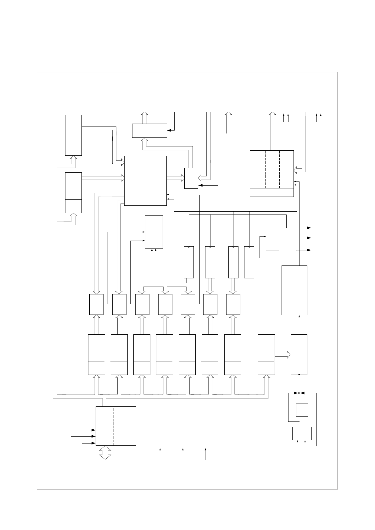
BLOCK DIAGRAM
MSM6255¡ Semiconductor
Start
Start
address
(upper)
SUAR
address
(lower)
SLR
15
- MA
0
MA
Linear
address
3-state
output
counter
Cursor
generation
circuit
ADF
MPX
counter
p
V
15
- A
0
A
DIEN
Duty counter
3
- RA
0
RA
Raster
address
Character
Shift clock sus-
counter
3
- UD
- LD
0
UD
LD
2-bit parallel
output
4-bit parallel
output
Timing
control
pension counter
3
0
CLP
8-bit parallel/
φ
CE
serial
φ
CH
7
- RD
0
RD
FRP
BUSY LIP
φ
CH
FRMB
RD
WR
CS
CMP
Cursor
address
CUP
Input register
7
- DB
0
DB
CMP
Cursor
address
CLR
Output register
R/W control
Instruction
register
CMP
Cursor
position
CPR
(upper)
CMP
Cursor
position
CPR
RES
(lower)
CMP
p
Number
of V
DPR
DD
V
CMP
Number
of duty
DUR
SS
V
CMP
Number of
characters hori-
zontal direction
HNR
p
Number
of H
PR
Timing generator
circuit for CHφ
PS and Load
Dot counter
Q
T
OSC
XT
XT
DIV
2/39
Page 3
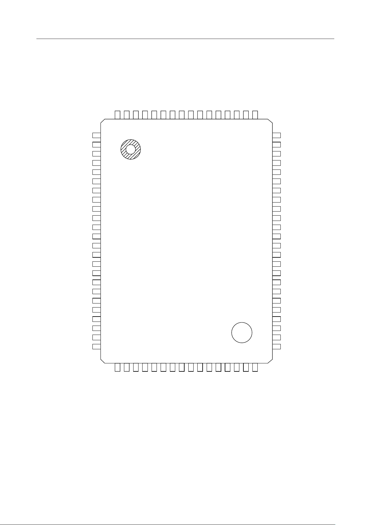
PIN CONFIGURATION (TOP VIEW)
10
6
MA
80
MA
79
9MA8
7
MA
MA
78
76
77
11
MA
75
12
MA
74
13
MA
73
14
MA
72
15
MA
71
DIV
70
2
TEST
69
1
TEST
68
V
67
SS
XT
66
MSM6255¡ Semiconductor
XT
65
MA
MA
MA
MA
MA
MA
A
A
A
A
A
A
FRP
LIP
1
5
2
4
3
3
4
2
5
1
6
0
7
15
8
14
9
13
10
12
11
11
12
10
13
A
9
14
A
8
15
A
7
16
A
6
17
A
5
18
A
4
19
A
3
20
A
2
21
A
1
22
A
0
23
24
64
RA
63
RA
62
RA
61
RA
60
RD
59
RD
58
RD
57
RD
56
RD
55
RD
54
RD
53
RD
52
DB
51 DB
50
DB
49
DB
48
DB
47
DB
46
DB
45
DB
44
RES
43
WR
42
RD
41
CS
3
2
1
0
7
6
5
4
3
2
1
0
7
6
5
4
3
2
1
0
25
CEf
26
CLP
31
30
29
28
27
3
2
1
0
LD
LD
LD
LD
FRMB
80-Pin Plastic QFP
32
V
DD
33
0
UD
34
1
UD
35
2
UD
36
3
UD
37
CHf
39
38
DIEN
BUSY
40
ADF
3/39
Page 4
PIN DESCRIPTIONS
Pin Symbol Type Description
1 - 6
71 - 80
7
22
23 FRP O
24 LIP O
25 CE
26 CLP O
27 FRMB O
28
31
32 V
33
36
37 CH
38 Busy O
39 DIEN I
40 ADF I
41 CS I
42 RD I
43 WR I
44 RES I
45
52
53
60
61
64
65
66
67 V
70 DIV I
MA
MA
A
LD
LD
UD
UD
DB
DB
RD
RD
RA
RA
A
DD
XT
XT
SS
15
0
O
15
0
Address output for displaying RAM.
MA
- MA15 are high impedance when ADF = "L".
0
Memory address input pins
I
Frame signal. Synchronization of display
Display data latch signal
φ
O
Chip enable clock for LCD segment driver
Display data shift clock
Alternate signal output pin
0
O
3
O
0
O
3
φ
O
Display data parallel output for lower side
Supply voltage
Display data parallel output, Upper display 4-bit output
(OD1, ED1, OD2 and ED2 outputs)
Character clock
Ready state signal. This signal is used while serial transmission stops.
Display enable signal. When this signal is "H", display is enabled.
Address floating input. When this signal is "L", MA0 - MA15, RA0 - RA3 are high impedance,
and when it is "H", A0 - A15 or a refresh address is output to MA0 - MA15.
Chip select. CS = "L"
Read. Reading data is valid when RD = "L"
Write. Data is written when WR = "H"
Reset. Resets each counter.
0
I/O
7
0
7
0
O
3
8-bit data bus. Common pins for 3-state I/O.
ROM/RAM data input. Dot pattern data for the character generator
I
Raster address output.
*This output is not used in the graphic mode.
RA
- RA3 are high impedance when ADF = "L".
0
I
X’tal osc. When an external clock is used by setting DIV to "H", feeds it to XT.
O
—
Ground pin.
"H" : EXT clock
"L" : Self oscillation
MSM6255¡ Semiconductor
4/39
Page 5
ABSOLUTE MAXIMUM RATINGS
Parameter Symbol Condition Rating Unit
Supply Voltage V
Input Voltage V
Storage Temperature T
DD
I
STG
Ta = 25°C –0.3 to +6 V
Ta = 25°C –0.3 to V
— –50 to +150 °C
RECOMMENDED OPERATING CONDITIONS
Parameter Symbol Condition Range Unit
Supply Voltage V
Operating Temperature T
Operating Frequency f
DD
op
osc
VSS = 0V 4.5 to 5.5 V
— –20 to +85 °C
VDD = 5V ±10% 0 to 11 MHz
ELECTRICAL CHARACTERISTICS
DD
MSM6255¡ Semiconductor
V
Input Characteristics
= 5V ± 5%, Ta = –20 to +85°C)
(V
DD
Parameter Symbol Min. Typ. Max. Unit Applicable pin
"H" Input Voltage V
"L" Input Voltage
"H" Input Voltage
"L" Input Voltage
"H" Input Current DB
"L" Input Current
"H" Input Current
"L" Input Current
IH
V
IL
V
IH
V
IL
I
IH
I
IL
I
IH
I
IL
2.4 — — V DB0 - DB7, CS, RD, WR, A0 - A15,
— — 0.7 V
DIEN, ADF, RD0 - RD7
4.5 — — V
RES, DIV, XT
— — 1.0 V
—— 1 mA
——–1mA
- DB7, CS, RD, WA, A0 - A15,
0
DIEN, ADF, RD
- RD7, RES, DIV
0
25 — 100 mA
TEST1, TEST2
——–1mA
Output Characteristics
= 5V ± 5%, Ta = –20 to +85°C)
(V
DD
Parameter Symbol Min. Typ. Max. Unit Applicable pin
"H" Output Current
"L" Output Current
I
OH
I
OL
Condition
V
= 2.8V
OH
V
= 0.4V
OL
–500 — — mA
2.4 — — mA
CHφ, CEφ, LIP, FRP
FRMB, BUSY, CLP
- LD
LD
0
UD0 - UD
MA0 - MA
RA0 - RA
DB
- DB
0
3
3
15
3
7
5/39
Page 6
Supply Current
= 5V ± 5%, Ta = –20 to +85°C)
(V
DD
Parameter Symbol V
Static Current I
Dynamic Current I
DDS
DD
DD
5f
5f
Condition Min. Typ. Max. Unit
= 0 Hz, no load — — 50 mA
osc
= 10 MHz, no load — — 15 mA
osc
Note: TEST 1 and TEST2 are open, and other inputs are either VDD or GND.
Switching Characteristics
MSM6255¡ Semiconductor
0.8 V
DD
0.2 V
DD
t
r
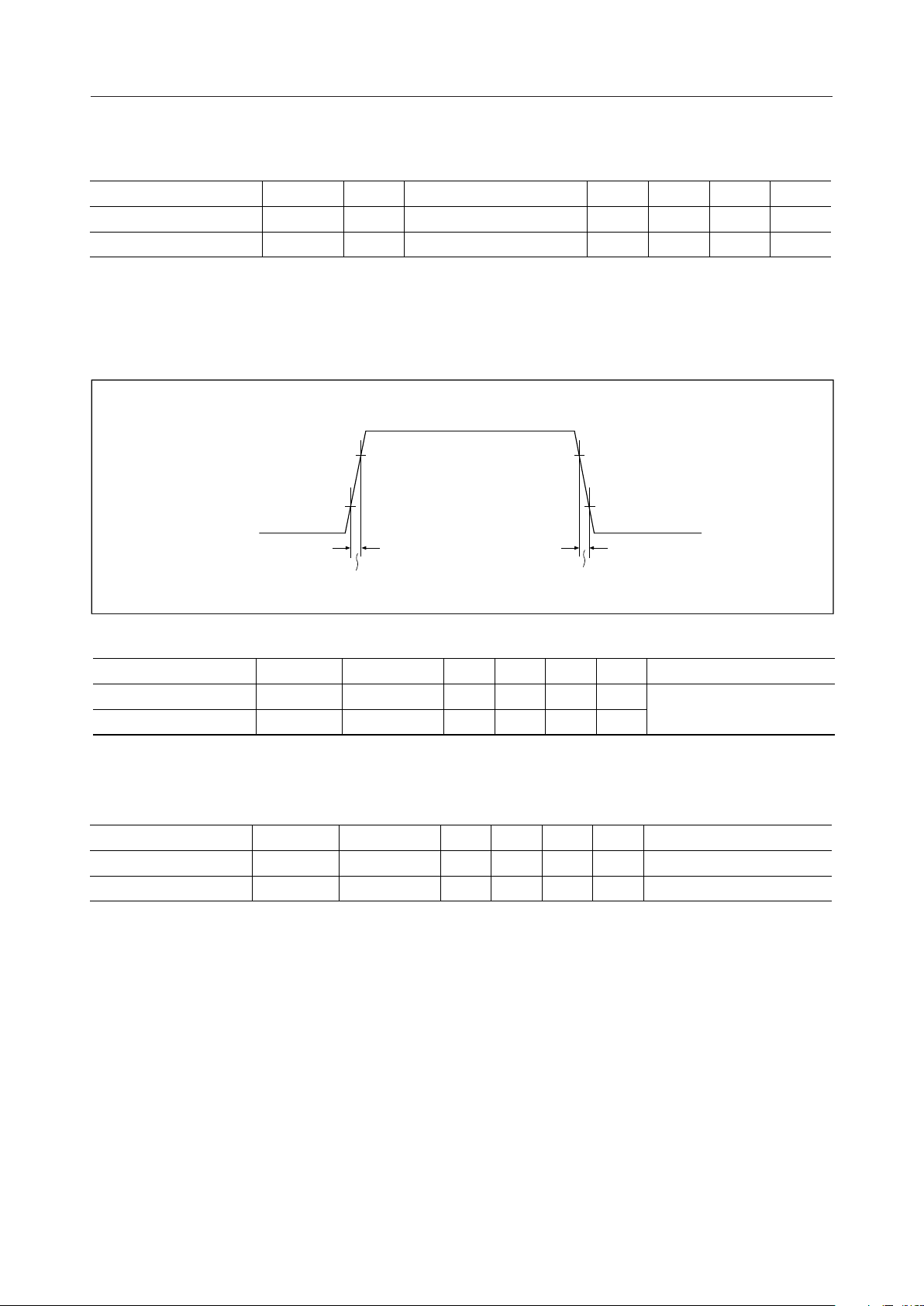
Parameter Symbol Min. Typ. Max. Unit Applicable pin
Rise Time t
Fall Time t
r
f
Condition
C
= 60 pF
L
— — 100 ns
— — 100 nsCL = 60 pF
0.8 V
t
f
DD
0.2 V
DD
= 5V ± 5%, Ta = –20 to +85°C)
(V
DD
All output pins
Operating Frequency
= 5V ± 5%, Ta = –20 to +85°C)
(V
DD
Parameter Symbol Min. Typ. Max. Unit Notes
Oscillating Frequency f
Basic Clock Frequency f
osc
s
Condition
DIV = "L"
——11MHz
— — 5.5 MHzDIV = "H"
Crystal oscillator
External clock
6/39
Page 7
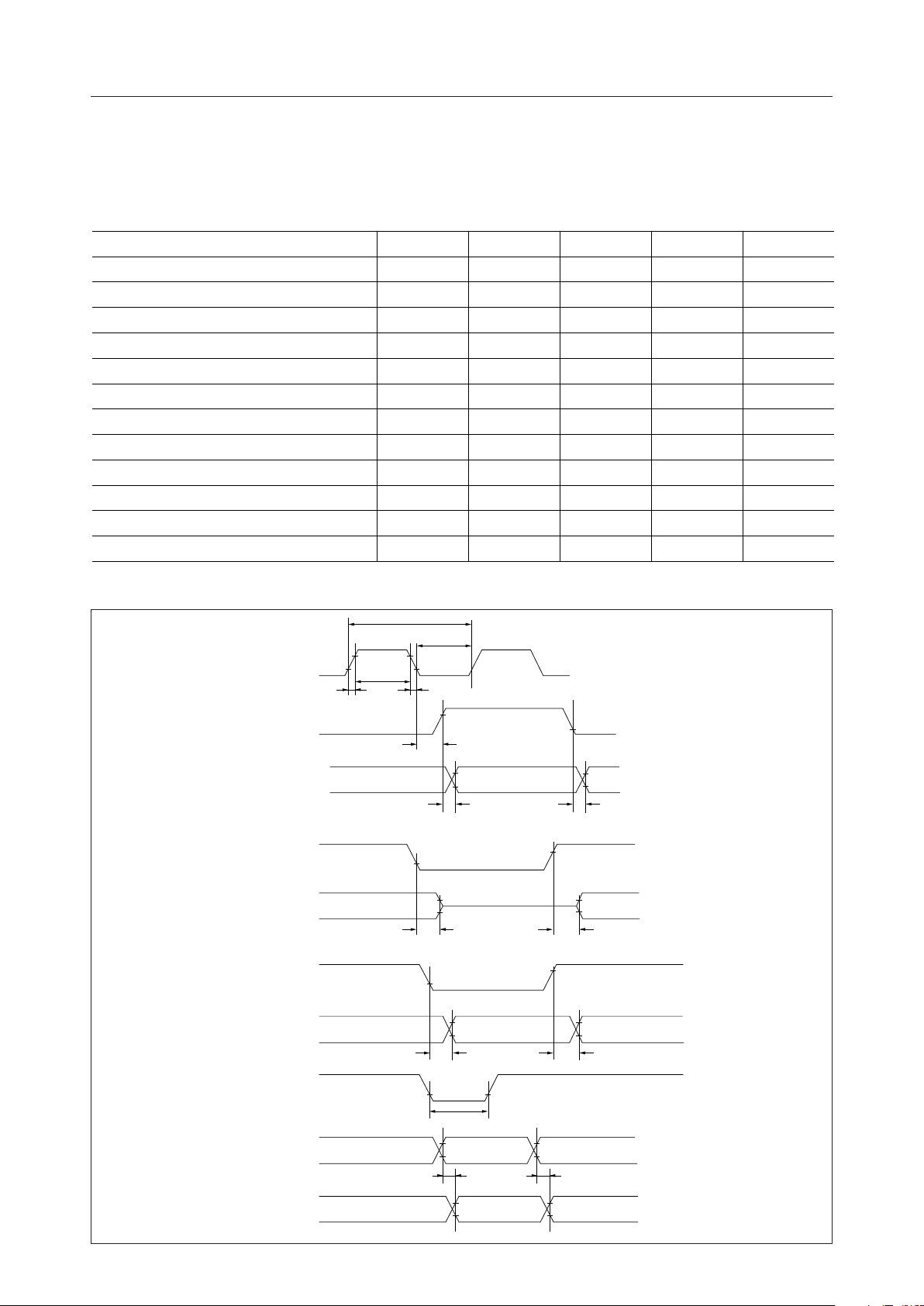
TIMING DIAGRAM
LCDC Control Signal Timing Characteristics
Parameter Symbol Min. Typ. Max. Unit
Clock Cycle Time t
Clock "H" Level Pulse Width P
Clock "L" Level Pulse Width P
Clock Rise/Fall Time t
Character Clock Delay Time t
Memory Address Clock Delay Time t
Memory Address Disable Delay Time t
Memory Address Enable Delay Time t
CPU Address Delay Time t
Refresh Address Delay Time t
Reset "H" Level Pulse Width t
CPU Address Delay Time t
CP
WH
WL
cr/tcf
CH
MA
AD1
AD2
AD3
AD4
RES
AD5
MSM6255¡ Semiconductor
= 30pF, VDD = 5V ± 5%, Ta = –20 to +85°C)
(C
L
180 — — ns
80 — — ns
80 — — ns
——20ns
— — 200 ns
— — 100 ns
——40ns
——40ns
— — 100 ns
— — 100 ns
1——ms
— — 100 ns
XT
(External clock)
CH
φ
MA0 - MA
15
ADF
MA0 - MA
15
RA0 - RA
3
DIEN
MA0 - MA
15
RES
t
CP
P
WL
P
WH
t
cr
Upper Side Address Lower Side Address
Refresh Address CPU Address Refresh Address
t
cf
t
CH
t
MA
VALID VALID
t
AD1
t
AD3
Floating
t
t
AD2
AD4
t
MA
A
- A
0
15
MA0 - MA
t
RES
t
AD5
15
t
AD5
7/39
Page 8
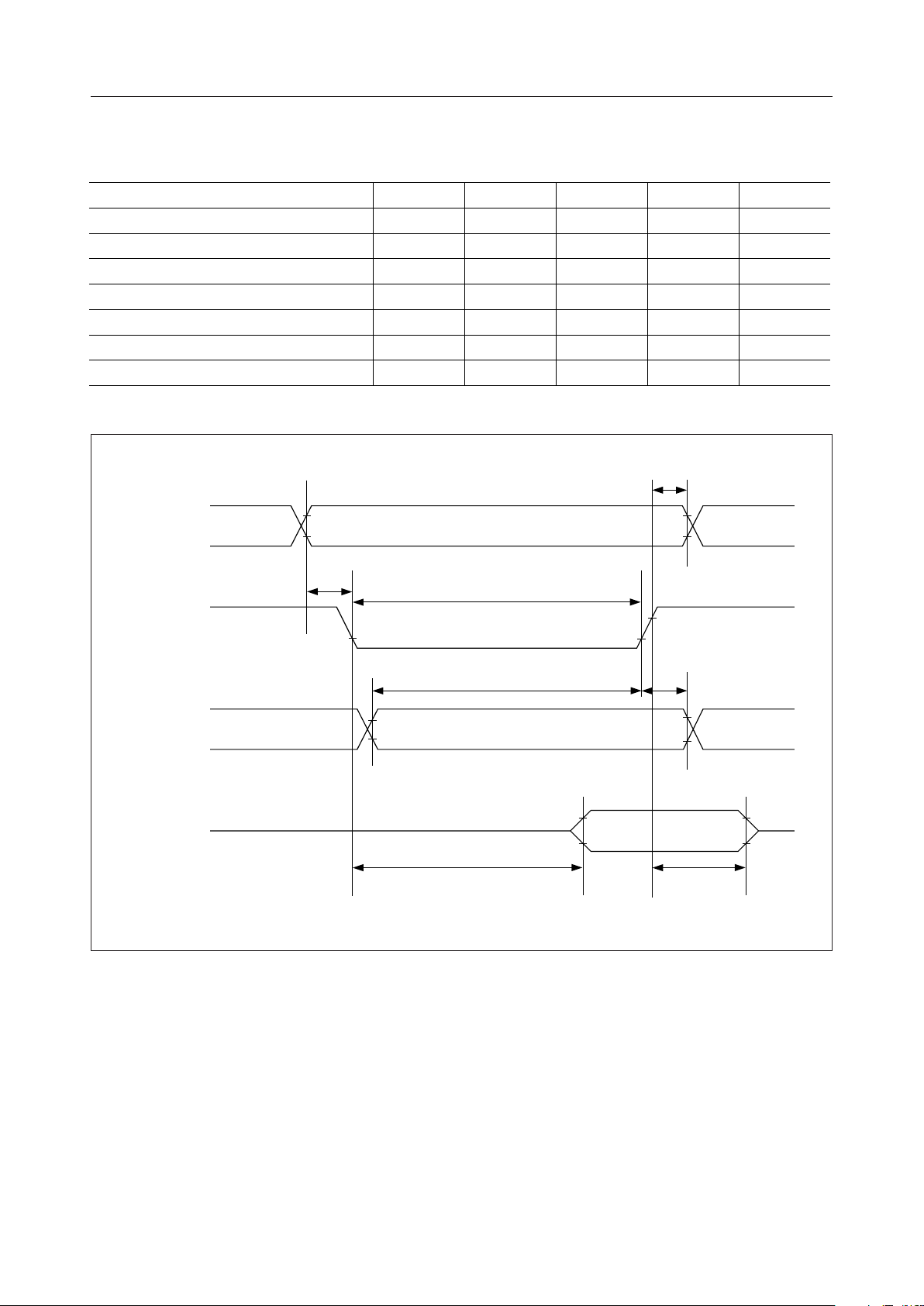
Bus Timing Characteristics
Parameter Symbol Min. Typ. Max. Unit
A
, CS Setup Time t
o
RD, WR Pulse Width t
Address Hold Time t
Data Setup Time t
Data Hold Time t
Output Disable Time t
Access Time t
A0, CS
CS
CW
AH
DS
DH
OH
ACC
MSM6255¡ Semiconductor
= 50pF, VDD = 5V ± 5%, Ta = –20 to +85°C)
(C
L
30——ns
200 — — ns
10——ns
60——ns
20——ns
0 — 40 ns
— — 200 ns
t
AH
WR, RD
- DB
DB
0
(WRITE)
DB
- DB
0
(READ)
t
cs
7
7
t
ACC
t
cw
t
DS
VALID
VALID
t
DH
t
OH
8/39
Page 9
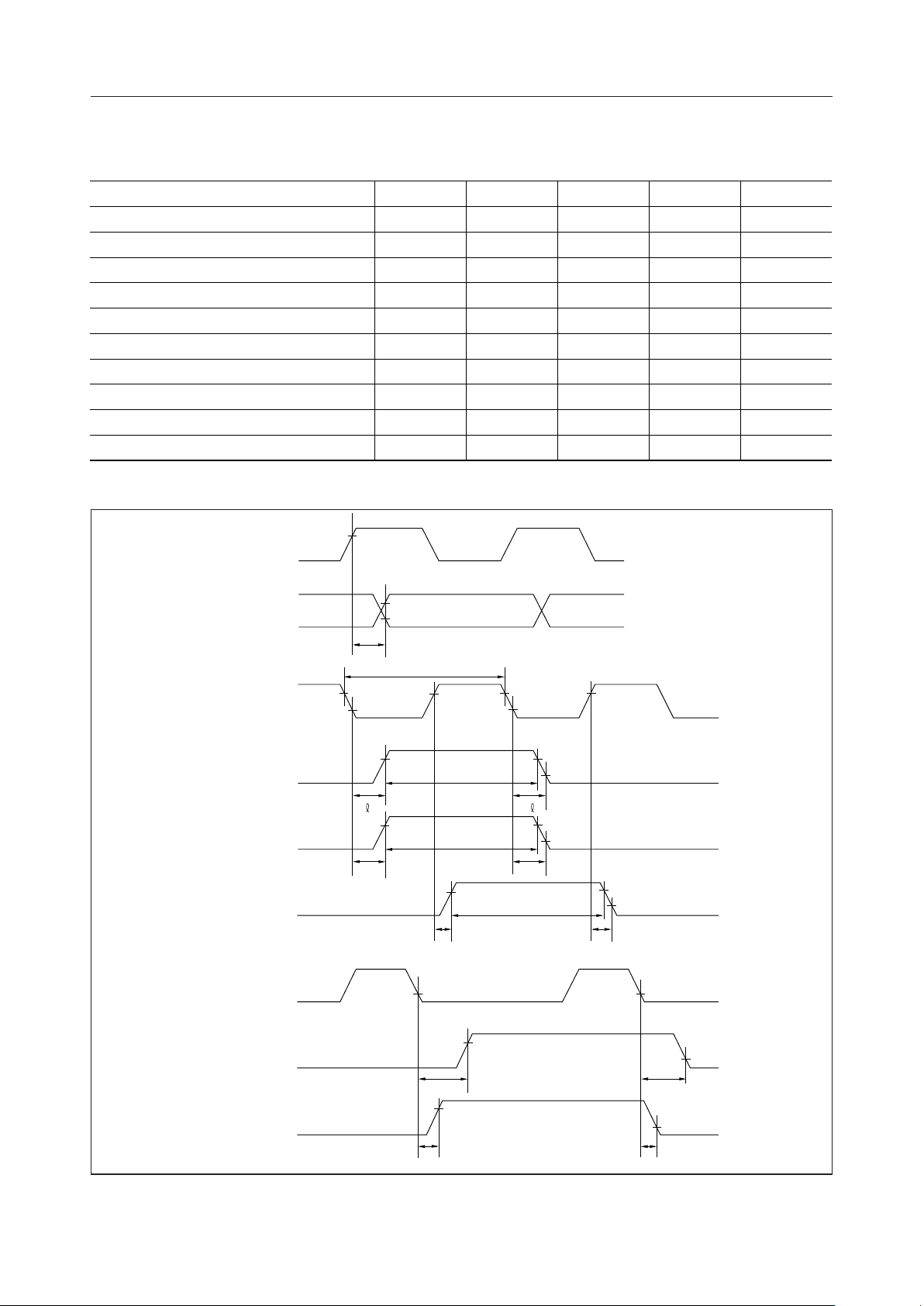
LCDC Driver Interface Timing Characteristics
Parameter Symbol Min. Typ. Max. Unit
Data Delay Time t
1 Character Cycle Time t
Latch Signal Delay Time t
Latch Signal "H" Time t
Chip Enable Clock Delay Time t
Chip Enable Clock "H" Time t
Ready Signal Delay Time t
Ready Signal "H" Time t
Frame Signal Delay Time t
Alternating Frame Signal Delay Time t
DA
CHφ
R
LIP
CE
CEφ
B
BUSY
FRP
FR
MSM6255¡ Semiconductor
(C
= 30pF, VDD = 5V ± 5%, Ta = –20 to +85°C)
L
— — 100 ns
730 — — ns
— — 200 ns
1.46 — — ms
— — 200 ns
730 — — ns
— — 200 ns
5.11 — — ms
2t
CHφ
— — 200 ns
—2t
+200 ns
CHφ
CLP
UD
0
LD
0
CHφ
LIP
CEφ
BUSY
LIP
- UD
- LD
3
3
t
DA
t t
t
CE
t
CHφ
t
LIP
t
CEφ
t
CE
t
BUSY
t
B
t
B
FRP
FRMB
t
FRP
t
FR
t
FRP
t
FR
9/39
Page 10
Timing for Fetching Pattern Data
Parameter Symbol Min. Typ. Max. Unit
Upper Side Data Setup Time t
Upper Side Data Hold Time t
Lower Side Data Setup Time t
Lower Side Data Hold Time t
CHφ
qw
UDS
UDH
LDS
LDH
MSM6255¡ Semiconductor
= 5V ± 5%, Ta = –20 to +85°C)
(V
DD
120 — — ns
0——ns
120 — — ns
0——ns
- MA
MA
0
RD0 - RD
15
7
Upper
side
Upper
side data
of q
t
UDS
Lower
side
t
UDH
t
Lower
side data
of q
LDS
Upper
side
t
LDH
Lower
side
Upper
side data
of w
Lower
side data
of w
10/39
Page 11
MSM6255¡ Semiconductor
FUNCTIONAL DESCRIPTION
LCDC Internal Registers
The internal registers include one instruction register (IR) and nine data registers. (See Table
1.)
Table 1 MSM6255 Internal Registers
Instruction
CS A
H X Invalid – –
register
0
3 2 1 0
X X X X
X X X XL H Instruction registerIR
L L L LL L Mode control register MOR X
L L L HL L Character pitch registerPR
L L H LL L
L L H HL L Duty number registerDVR
L H L LL L Cursor form registerCPR
L H L HL L
L H H LL L
L H H HL L
H L L LL L
Register Register name
–
HNR
SLR
SUR
CLR
CUR
Horizontal character number
register
Start address (lower) register
Start address (upper) register
Cursor address (lower)
register
Cursor address (upper)
register
X
Note: "L" is read if the data of the registers marked X is read.
WRITEREAD
7
X
X
X
Data bit
5432106
XXX
X
– Instruction register
The instruction register is a register for specifying the address of the data register which is
accessed.
This register is cleared when RES input is "L".
11/39
Page 12
– Mode control register
The mode control register is specified by writing "00H" in the instruction register.
MSM6255¡ Semiconductor
Register
Instruction register
Mode control register
D
D
6
D
5
D
4
H/L H/L H/L H/L
D
3
LL
HL
XH
XH
LL
HL
XH
XH
A
D
0
D
7
D
6
D
5
D
4
D
3
D
2
D
1
0
HLLLLLL LL
L L MODE DATA
D
2
D
1
0
Output mode
1-bit serial
2-bit parallel
L
Character display
4-bit parallel
1-bit serial
2-bit parallel
H
Graphics
4-bit parallel
Blink time
Cursor
ON/OFF
Cursor blink
Display
ON/OFF
2-bit parallel
4-bit parallel/
1-bit serial
Mode
H: Display ON
L: Display OFF
D
D
5
4
L L Cursor OFF
L H Cursor OFF
H L Cursor ON
H H Cursor blink
H: 16 frames
L: 32 frames
Half of blinking cycle
12/39
Page 13

– Character pitch register
MSM6255¡ Semiconductor
Register A
Instruction register H L
Character pitch register L
D
0
D
7
D
6
L
(V
– 1)
p
L
D
5
D
4
L
D
3
L
L
D
2
L
(H
p
1
L
– 1)
D
0
H
Hp represents the number of bits to be displayed among one byte display data sent from RAM.
The value of Hp is the following five types.
H
p
4LHH
5H L L
6H LH
7HHL
8HHH
D
2
D
1
D
0
– Horizontal character number register
Register A
Instruction register H L
Character number register L
D
0
D
7
L
D
6
L
D
5
L
D
4
L
(H
N
3
L
– 1)
D
D
2
L
D
1
H
0
L
Assuming that the total horizontal dot number of the display is nH,
nH = Hp x HN, where HN = 2 to 128.
The maximum value of nH = 8 x 128 = 128 bytes = 1,024 dots.
– Duty number register
Register A
Instruction register H L
Time division register L
D
0
D
7
D
6
L
D
5
L
4
L
(N
Nx = 2 to 256
– Cursor form register
Register A
Instruction register H L
Cursor position register L
D
0
D
7
L
(C
D
6
– 1)
pu
D
5
L
4
L
– 1)
X
D
D
3
L
D
D
3
L
D
2
L
D
2
H
(C
– 1)
pd
D
1
H
1
L
0
H
D
0
L
The cursor is displayed on the lines from Cpu to Cpd in the character display mode. The length
of the cursor in the horizontal direction is equal to the character pitch in the horizontal direction,
Hp. The cursor is not displayed in graphic mode. The relation between the cursor and Vp is as
follows.
13/39
Page 14

Font configuration of Hp = 7 and Vp = 8
MSM6255¡ Semiconductor
0
1
2
3
4
5
6
7
0
1
2
3
4
5
6
7
Cpu = 8, Cpd = 8 Cpu = 7, Cpd = 8
Notes: (1) Setting of Cpu, Cpd > Vp is not available.
(2) The cursor signal and pattern data are displayed subject to EX-OR.
– Start address (lower) register
Register A
Instruction register H L
Display start address register (lower byte) L
D
0
7
0
1
2
3
4
5
6
7
Cpu = 2, Cpd = 6
D
D
6
L
D
5
L
D
4
L
D
3
L
D
2
H
D
1
L
0
H
Start address (lower)
– Start address (upper) register
Register A
D
0
Instruction register H L
Display start address register (upper byte) L
D
7
D
6
L
D
5
L
D
4
L
D
3
L
D
2
H
D
1
H
0
L
Start address (upper)
The display start address shows an address of the RAM which stores data displayed at the left
end and the most upper position. The start address is composed of upper and lower 8 bits (16
bits in total).
– Cursor address (lower) register
Register A
D
0
Instruction register H L
Cursor address register (lower byte) L
D
7
D
6
L
D
5
L
D
4
L
D
3
L
D
2
H
D
1
H
0
H
Cursor address (lower)
– Cursor address (upper) register
Register A
Instruction register H L
Cursor address register (upper byte) L
D
0
D
7
D
6
L
D
5
L
D
4
L
D
3
H
D
2
L
D
1
L
0
L
Cursor address (upper)
By this instruction, the value of the cursor address is written in the cursor address register. The
cursor is displayed at the position specified by the cursor address register.
14/39
Page 15

MSM6255¡ Semiconductor
H
N
V
(Upper)
V
(Lower)
RD
p
V
H
7
p
RD
0
C
pu
C
pd
Symbol
H
p
V
p
H
N
V
C
pu
C
pd
Fig. 1 Cursor Address (Upper) Register
Name Meaning Value
Horizontal pitch
Vertical pitch
Number of characters in one line
Number of rows
Cursor start position
Cursor end position
Table 2 Legend
Pitch of characters in horizontal
direction
Pitch of characters in vertical
direction
Number of characters per line or
number of words per line
Display duty
A position where the cursor starts
display
A position where the cursor stops
display
4 - 8 dots
1 - 16 dots
2 - 128 characters
2 - 256
Line 1 - 16
Line 1 - 16
15/39
Page 16

MSM6255¡ Semiconductor
– Built-in Bus Averter
The bus averter which switches the address buses A0 - A15 of the CPU with the memory
address buses of the refresh. The refresh memory addresses are output to MA0 - MA15 when
the DIEN pin is set at high level and A0 - A15 are output to MA0 - MA15 when the DIEN pin
is set at low level.
– External Clock Operation
An external clock enables the MSM6255 to operate when the DIV pin is set at high level. Input
the external clock to XT.(Leave XT open.)
When the DIV pin is set at low level, the IC enters the crystal oscillation mode.
– Address Output Floating
MA0 - MA15 and RA0 - RA3 become high impedance when the ADF pin is set at low level.
MA0 - MA15 and RA0 - RA3 become normal impedance when the ADF pin is set at high level.
– Power Down Function
The chip select function becomes enabled for the segment driver by connecting the CEf pin
to the ECLK input of the MSM5279. The power down function is valid only in 4-bit parallel
output mode.
– Refresh Memory Address (MA0 - MA15) Operation
In the horizontal direction, MAxx is counted up at the falling edge of CHf. Upper side is
addressed while CHf is set at low level and lower side is addressed while CHf is set at high
level.
MAxx is counted up even if it exceeds the number of horizontal display characters, but this
does not affect the display since no data is being transferred at the time.
The period in which the data transfer is suspended corresponds to eight characters. When the
period passes, one horizontal cycle is completed and the next cycle is commenced.
Memory address operation in the graphic mode is shown in Fig. 2 and that in the character
mode is shown in Fig. 3.
16/39
Page 17

Address configuration of display RAM
MSB LSB
MA14MA13MA12MA11MA10MA9MA8MA7MA6MA5MA4MA3MA2MA1MA
MA
15
H
N
1 word
0000 0001 004E 004F
0050 0051 009E 009F
1EF0 1EF1 1F3E 1F3F
1F40 1F41 1F8E 1F8F
1F90 1F91 1FDE 1FDF
Suspension of
data transfer
Upper
Lower
MSM6255¡ Semiconductor
0
3E30 3E31 3E7E 3E7F
Fig. 2 Memory Address in Graphic Mode (640 x 200)
Note: "L" is output for RA0 - RA3.
17/39
Page 18

Line 1
Line 2
Raster
address
000
001
010
011
100
101
110
111
000
111
HN (Number of characters in horizontal display line)
1 character
0000
0000
0000
0050
0050 0051 009E 009F
0001
0001
0001
0051
004E
004E
004E
009E
004F
004F
004F
009F
MSM6255¡ Semiconductor
Suspension of
data transfer
Upper
Line 12
Line 13
0370 0371 03BE 03BF
000
0370
111
000
03C0
03C0 03C1 040E 040F
111
0730 0731 077E 077F
000
0371
03C1
03BE
040E
03BF
040F
Lower
Line 24
0730 0731 077E 077F
111
Note : Start address is 0000, 80 characters x 24 lines and V
Fig. 3 Memory Address in Character Mode (80 characters x 24 lines)
p
= 8
18/39
Page 19

MSM6255¡ Semiconductor
– Output Mode
Three kinds of modes, 1-bit serial, 2-bit parallel and 4-bit parallel, are available as output
modes. Data flows of each mode are shown below.
Segment
driver
Segment
driver
Data shift
Upper
Lower
Data shift
Fig. 4 1-Bit Serial Data Transfer
Data shift
LCD panel
UD
UD
UD
UD
0
1
1
0
Upper
LCD panel
Lower
Data shift
Fig. 5 2-Bit Parallel Data Transfer
UD
UD
2
3
19/39
Page 20

MSM6255¡ Semiconductor
CE
4
3
φ
UD0 - UD
Upper
LCD panel
Lower
- LD
LD
0
3
4
Fig. 6 4-bit Parallel Data Transfer
Time charts corresponding to data transfers shown in Fig. 4 - Fig. 6 are shown in Fig. 7 - Fig. 9.
fs, the dot clock, shown in Figs.7-9, is a signal inside the IC. For more information see "Relation
between Reference Clock (fs) and External Clock" on page 601.
20/39
Page 21

MSM6255¡ Semiconductor
STAN STAM STAN+1 STAM+1ENDMENDN
0
654321D
7
D
0
654321D
7
D
0
STAN+1 data
654321D
7
D
0
STAN data
654321D
7
D
STAM+1 data
STAM data
Fig. 7 1-bit Serial Data Transfer
ENDN data
0
Suspension of data transfer
654321D
7
D
s
f
φ
CH
15
MA
0
CLP
0
UD
0
654321D
7
D
1
UD
ENDM data
STAN: First memory address of one horizontal line in the upper side
STAM: First memory address of one horizontal line in the lower side
ENDN: Last memory address of one horizontal line in the upper side
ENDM: Last memory address of one horizontal line in the lower side
MA
21/39
Page 22

MSM6255¡ Semiconductor
STAM+1STAN+1STAMSTANENDMENDN
1
D
3
D
5
D
7
D
1
D
3
D
5
D
7
D
0
D
2
D
4
D
6
D
0
D
2
D
4
D
STAN data STAN+1 data
6
D
1
D
3
D
5
D
7
D
1
D
3
D
5
D
7
D
0
D
2
D
4
D
6
D
0
D
2
D
4
D
STAM data STAM+1 data
6
D
Fig. 8 2-bit Parallel Data Transfer
ENDN data
ENDM data
1
D
3
D
5
Suspension of data transfer
s
f
φ
CH
15
MA
0
CLP
D
D
7
0
UD
0
D
2
D
4
D
6
D
1
UD
D
D
D
D
1
3
5
7
2
UD
0
D
2
D
4
D
6
D
3
UD
STAN: First memory address of one horizontal line in the upper side
STAM: First memory address of one horizontal line in the lower side
ENDN: Last memory address of one horizontal line in the upper side
ENDM: Last memory address of one horizontal line in the lower side
MA
22/39
Page 23

MSM6255¡ Semiconductor
3
D
7
D
3
D
7
D
2
D
6
D
2
D
6
D
1
D
5
D
1
D
5
D
0
D
4
D
0
D
4
D
3
D
7
D
3
D
7
D
2
D
6
D
2
D
6
D
1
D
5
D
1
D
5
D
0
D
4
D
0
D
4
D
Fig. 9 4-bit Parallel Data Transfer
Suspension of data transfer
3
D
7
D
3
D
7
D
2
D
6
D
2
D
6
D
1
D
5
D
1
D
5
D
0
D
4
D
0
D
4
D
ENDN ENDM ENDN+1 ENDM+1 STAN STAM STAN+1 STAM+1
s
f
φ
CH
15
- MA
0
MA
CLP
3
UD
2
UD
1
UD
0
UD
3
D
7
D
3
D
7
D
ENDN-1 data ENDN data STAN data STAN+1 data
3
UD
2
D
6
D
2
D
6
D
2
UD
1
D
5
D
1
D
5
D
1
UD
0
D
4
D
0
D
4
D
0
UD
ENDM-1 data ENDM data STAM data STAM+1 data
23/39
Page 24

MSM6255¡ Semiconductor
– Relation Between Duty and Number of Lines
Number of lines is determined by Vr, number of lines in vertical direction(display duty).
Number of lines = Vr x 2
Note: In the character display mode, number of lines should not be odd number.
– Calculation of Crystal Oscillation Frequency (f
Table 3 Calculation Formula of f
DIV Output mode Calculation formula of f
L
q FRP x (H
w FRP x (H
q FRP x (H
H
w FRP x (H
+ 8) x Hp x Vr x 2 9.856
N
+ 8) x Vr x 4 2.464
N
+ 8) x Hp x V
N
+ 8) x Vr x 2 1.232
N
osc
)
osc
osc
r
Calculation exmaple (MHz)
4.928
Note: (1) Table 3 shows a calculation example assuming that FRP = 70 Hz, HN = 80, Hp = 8 and
Vr = 100. However, the example of Hp = 4 to 7 in 4-bit parallel is not included.
(2) Output mode q :Hp = 4 to 7 in 1-bit serial, 2-bit parallel and 4-bit parallel
Output mode w :Hp = 8 in 4-bit parallel
– Calculation of Character Clock (CHf) Frequency
CHφ = FRP x (HN + 8) x V
r
Example: Assuming FRP = 70 Hz, HN = 80 and Vr= 100, CHf = 1.62 (ms)
– Calculation of Shift Clock (CLP) Frequency
Table 4 Calculation Formula of CLP
Output mode Calculation formula of CLP Calculation exmaple (MHz)
1-bit serial RP x (H
2-bit parallel FRP x (H
4-bit parallel FRP x (H
+ 8) x Hp x Vr 4.928
N
+ 8) x Hp x Vr x 1/2 2.464
N
+ 8) x Hp x Vr x 1/4 1.232
N
Note: Table 4 shows a calculation example assuming that FRP = 70 Hz, HN = 80, Hp = 8 and
Vr= 100.
24/39
Page 25

– Relation Between Reference Clock (fs) and External Clock
DIV
XT
Q
XT
XT
T
MSM6255¡ Semiconductor
f
s
f
s
(DIV = 1)
fs functions as a dot clock in LCDC and the dot counter inside the IC is counted up at the trailing
edge of fs.
The dot counter operates as a N-ary counter on a basis of HP and generates the character clocks
(CHf).
(Refer to the time charts Fig. 7 - 9 and Fig. 14.)
– Access to the Display RAM
In writing/reading the data to/from the display RAM, DIEN should be low level. By setting
DIEN signal at low level, the address from the CPU are output from MA0 - MA15, and this
enables the access to the display RAM.
There are three methods of accessing display RAM from the CPU.
(1) Direct access from CPU
Display RAM is accessed directly from the CPU, irrespective of the condition of MSM6255
(refresh cycle or not).
In this method, the RAM address changes to the CPU address when the display is on the
screen. So, frequent access to the RAM causes flickering on the screen.
(2) Access while BUSY signal is high
BUSY signal indicates the period when the data transfer stops, and BUSY signal is set high
when the data transfer stops. The period when BUSY signal is high corresponds to that of
seven characters’. If display RAM is accesed during this period (when BUSY is high), the
display on the screen does not flicker.
Note: This method is effective when the size of screen is small. In the case of big size
screen, 640 x 200 dots, 1character needs approx. 1.6ms. So, in this case, the period
when BUSY is at high level is 11.2ms, which is impossible to write or read a lot of
data.
(3) Synchronized access (only for operating the IC by external clock)
Refresh cycle and CPU cycle are alternately performed. So, there is not flickering on the
screen and there is no need to sense the BUSY signal.
When using this method, however, some external circuitry is necessary. The timing chart
of this method is described in the Figure 10 below.
25/39
Page 26

CH
MSM6255¡ Semiconductor
φ
DIEN
display
RAM
OUT
T
C
CPU LCDC CPU LCDC CPU LCDC CPU LCDC
t
RAM
T
L
fetching the
pattern data
t
UDS
t
MN
UDH
N + 1 M + 1
Fig. 10 Basic Timing of Synchronized Access to Display RAM
Legend
T
C
T
L
t
RAM
t
UDS
t
UDH
: Period when the address bus is occupied by CPU
: Period when the LCDC fetches the refreshed data
: Refresh address delay time + memory access time
: Upper side data set-up time
: Upper side data hold time
When DIEN is high, MA0 - MA15 output address to the upper side when CHf is low and to the
lower side when CHf is high.
To perform synchronized access method, the timing between DIEN and CHf should be as
described in Figure 10.
WR
V
DD
PR
DQ
PR
DQ
PR
DQ
PR
DQ
M-WR
M-RD
V-RAM
CL
Q
CL
Q
CL
Q
CL
Q
SELECT
DIEN
READY
DATA LATCH
Fig. 11 Wait Function Controlling Circuit
Display RAM must meet the following condition:
TL > t
RAM
+ t
UDS
In writing data into the display RAM, LCDC should be synchronized so that the write pulse
occurs during the period of TC. In reading the pattern data from the CPU, the data of display RAM
should be latched first.
Figure 11 shows the controlling circuit.
26/39
Page 27

MSM6255¡ Semiconductor
)
– DIEN
DIEN has to be generated when the display RAM is accessed by Synchronized access method.
(1) When the LCD screen is not split into upper and lower ones
If, for example, an LCD panel with a total of 64 dots in vertical direction is displayed at
1/64 duty, either the upper side data or the lower side data becomes unnecessary, and
then the CHf signal can be used as a DIEN signal.
(2) When the LCD screen is split into upper and lower ones
If 4-bit parallel output mode is set and HP=8, the timing diagram of the dot clock and the
character clock is as shown below.
XT
(dot clock)
CH
φ
t
CH
DIEN signal is generated by XT and CHφ.
DIEN signal generating circuit is shown below.
DIEN
D Q
φ
Q
XT(dot clock
When H
CH
π 8 in the 1-bit serial, 2-bit parallel and 4-bit parallel mode, the relation between
p
XT and CHφ should be referred to Figures 7 and 8.
– Scroll◊Paging
Scroll◊paging is enabled by setting the display start address to the scroll address register.
(1) Memory address of vertical scroll◊paging
Figure 2 shows the memory address when the start address is 0000. When the start address
is set at 0050, the display will be vertically shifted by +1.
By setting the starting address one by one, the screen will scroll vertically.
paging will be performed by setting the start address as 3E80.
(2) Memory address of horizontal scroll
When the starting address is set at 0001 in Figure 2, the display on the screen will be shifted
by +1 byte horizontally. The data shown as 004F in Figure 2 corresponds to the memory
data in the 2nd line shown as 0050.
27/39
Page 28

APPLICATION CIRCUITS
Interface With CPU
MSM6255¡ Semiconductor
MSM6255
8085
AD
0
A
WR
IO/M
- AD
ALE
HLDA
- A
8
RD
15
WR
RD
A1 - A
7
OC
Decoder
7
CS
- DB
DB
0
A0 - A
7
15
Z80
IORQ
- D
D
0
A0 - A
WR
RD
15
MSM6255
WR
RD
A1 - A
7
Decoder
7
CS
- DB
DB
0
A0 - A
7
15
28/39
Page 29

MSM6255¡ Semiconductor
MSM6255
8086
M/IO
DT/R
DEN
AD0 - AD
A
- A
16
BHE
ALE
*Minimum mode
15
19
Transceiver
Latch
D0 - D
A0 - A
WR
RD
A1 - A
15
BHE
19
Decoder
15
D
- D
1
7
CS
DB0 - DB
- A
A
0
15
7
6800
VMA
RD/WR
D0 - D
A0 - A
MSM6255
φ
2
RD
WR
Decoder
CS
DB
- DB
0
A0 - A
7
15
15
A1 - A
15
7
29/39
Page 30

System Configuration
MSM
5299C
MSM6255¡ Semiconductor
CS RD WR
0
UD
- DB
DB
~
7
0
4 bit
3
UD
MSM
6698
CLP
φ
CE
LIP
FRP
FRMB
3
- LD
0
LD
15
- MA
0
MA
15
- A
0
A
DIEN
7
- RD
0
RD
MSM6255
Fig. 12 System Configuration in Graphic Mode
40H245
15
- A
I/O
B
A
Display
RAM
WR
0
A
CPU
Decoder
30/39
Page 31

MSM
MSM6255¡ Semiconductor
5299C
CS RD WR
0
UD
4 bit
~
3
UD
CLP
7
- DB
0
RD
φ
CE
MSM
LIP
3
- RA
0
RA
Character
generator
6698
FRP
FRMB
MSM6255
DIEN
7
- DB
0
DB
Display
WR
15
- MA
0
MA
RAM
15
- A
0
A
Fig. 13 System Configuration in Character Mode
CPU
DIEN
Decoder
31/39
Page 32

MSM6255¡ Semiconductor
32/39
N N + 1 N + 2 STA STA STA STA STA STA STA STA + 1 STA + 2 STA + 3
CH
T
BUSY
T
CEφ
T
LIP
Start address
f
s
Memory
address
LIP
BUSY
FRP
CE
φ
CH
φ
T
s
Fig. 14 Timing Chart During Suspension of Shift Clock
CH = T
s
x Hp
T
LIP
= 2CH
T
CEφ
= CH
T
BUSY
= 7CH
Condition : 4-bit parallel output mode
H
P
= 5
Page 33

MSM6255¡ Semiconductor
33/39
Fig. 15 Timing Chart of LIP, FRP and FRMB
Y
1
Y
2
Y
N
Line N Line 1 Line 2X driver
Y driver
•••••••• •• ••••• •• •••••••••••••••
Line 1 Line 2
Suspension of
shift clock
FRMB
FRP
LIP
Memory
address
– – –
Page 34

LIP
CLP
Counter
(Inside the IC)
CEf
Carry output
of segment driver
MSM6255¡ Semiconductor
012190
Valid
Fig.16 Timing Chart of CLP and CEf
34/39
Page 35

MSM6255¡ Semiconductor
Figures 17-1, 17-2, and 18 show application circuits.
In these examples, the size of LCD module is 640 x 200 dots.
4-bit data transfer is applied and Hp = 8.
The synchronized access method is used as a method of access to the display VRAM.
VRAMSEL
.
.
.
.
M RD
M WR
IO RD
IO WR
1Y2Y3Y
HC257
4Y
G
1A3B2A4B1B2B3A4ASEL(A)
+5V
9
ADR- 5ADR-14ADR-13ADR-12ADR-11ADR-10ADR-
+5V
LCDC-CS
0
1
2
3
Y
HC138
ABC
ADR- 8ADR-7ADR-6ADR-5ADR-4ADR-3ADR-2ADR-1ADR-
HCT373
4
A
B
2
2
G
G
0
Q
D
PR
DQ
5
6
7
1
G
OE
CL
+5V
7
6
.
.......
D BUS-
D BUS-
D BUS-5D BUS-4D BUS-3D BUS-2D BUS-1D BUS-
B
HCT245
A
CLK
RES
CLK-OUT
Q
PR
+5V
0
CL
HC74
DQ
HC04
Fig. 17-1
OE
DIR
15
14 13 12 11 9
A
2
X1X
50 pF
50 pF
6.144 MHz
8
7
6 5 4 3 2 1
D
80C85A
+5V
READY
0
ALE
RST-IN
51 kW
2.2µF
SW
RESET
RD
WR
CLK
IO/M
READY
RSTOUT
35/39
Page 36

MSM6255¡ Semiconductor
φ
UD0UD1UD2UD3LD0LD1LD2LD
CH
RES
MA0MA1MA2MA3MA4MA5MA6MA7MA8MA9MA10MA11MA12MA
MSM5165
A0A1A2A3A4A5A6A7A8A9A10A11A
MSM5165
LCD
15
ADR-0ADR-1ADR-2ADR-3ADR-4ADR-5ADR-6ADR-7ADR-8ADR-9ADR-10ADR-11ADR-12ADR-13ADR-14ADR-
+5V
3
FRP
FRMB
φ
LIP
CE
CIP
A0A1A2A3A4A5A6A7A8A9A10A11A12A13A14A
DIV
ADF
15
MSM6255
13
RD0RD1RD2RD3RD4RD5RD6RD
1
CE
WE
OE
HC04
1
12
CE
0
WE
OE
1 2 3 4 5 6
D
7
DB0DB1DB2DB3DB4DB5DB6DB7DIENXTCSRDWR
7
+5V
Q
RP
HC74
DQ
Q
RP
HC74
DQ
Q
RP
HC74
DQ
HC08
HC08
HC04
HC04
Fig. 17-2
HCT244
CL
+5V
HC08
CL
CL
HC86
QD
PR
HC08
+5V
HC00
2
G1G
AY
Q
CL
HC74
+5V
HCT374
QD
HC32
OE
HC32
HC32
HC32
HC32
HC04
ADR-14
ADR-15
M-WR
M-RD
RES
READY
VRAMSEL
CLK-OUT
0
.......
D BUS-
D BUS-1D BUS-2D BUS-3D BUS-4D BUS-5D BUS-6D BUS-
7
CLK
.
IO-RD
LCDC-CS
IO-WR
36/39
Page 37

30pF
XT
2.5 MHz
XT
MSM6255¡ Semiconductor
DIV
12
- MA
0
MA
15
- MA
0
MA
ADF
15
- MA
12
MA
- A
A
15
0
RES
7
- DB
0
CS
DB
BUSYRDWR
DIEN
7
- RD
0
RD
3
- RA
0
RA
MSM6255
MAM5165RS
(8K x 8 bit)
for CGROM
5V5V5V5V
8
11
~
A
A
A
LS245
OE
7
- A
0
A
12
CE
LS244
AY
RD
7
- DO
0
DO
1G 2G
→
A
B
“H” =
DIR
B
A
G
LS125
1
DB
LS74
CK
DQ
4
2764
8
- I/O
1
I/O
8
- I/O
1
I/O
8
- I/O
1
I/O
8
- I/O
1
I/O
7
~ DO
0
DO
WE
WE
WE
WE
1
2
OE
CE
CE
12
- A
0
A
1
2
OE
CE
CE
12
- A
0
A
1
2
OE
CE
CE
12
- A
0
A
1
2
OE
CE
CE
12
- A
0
A
OE
12
- A
0
A
CE
LS13B
7
Y
6
Y
5
Y
4
Y
3
Y
2
Y
1
Y
0
Y
5V
7
Y
5
Y
0
Y
5V
- MA
13
MA
Fig. 18
G2A G2B
G1
LS13B
15
- A
11
A
A~B A~B
G2A G2B
G1
12
- A
0
A
for software
7
- DB
0
DB
RD
WR
MREQ
Z80
- A
A
15
0
RES
37/39
Page 38

PACKAGE DIMENSIONS
QFP80-P-1420-0.80-K
Mirror finish
MSM6255¡ Semiconductor
(Unit : mm)
Package material
Lead frame material
Pin treatment
Solder plate thickness
Package weight (g)
Epoxy resin
42 alloy
Solder plating
5 mm or more
1.27 TYP.
Notes for Mounting the Surface Mount Type Package
The SOP, QFP, TSOP, SOJ, QFJ (PLCC), SHP and BGA are surface mount type packages, which
are very susceptible to heat in reflow mounting and humidity absorbed in storage.
Therefore, before you perform reflow mounting, contact Oki’s responsible sales person for the
product name, package name, pin number, package code and desired mounting conditions
(reflow method, temperature and times).
38/39
Page 39

QFP80-P-1420-0.80-BK
Mirror finish
MSM6255¡ Semiconductor
(Unit : mm)
Package material
Lead frame material
Pin treatment
Solder plate thickness
Package weight (g)
Epoxy resin
42 alloy
Solder plating
5 mm or more
1.27 TYP.
Notes for Mounting the Surface Mount Type Package
The SOP, QFP, TSOP, SOJ, QFJ (PLCC), SHP and BGA are surface mount type packages, which
are very susceptible to heat in reflow mounting and humidity absorbed in storage.
Therefore, before you perform reflow mounting, contact Oki’s responsible sales person for the
product name, package name, pin number, package code and desired mounting conditions
(reflow method, temperature and times).
39/39
 Loading...