

Page 1

¡ Semiconductor MSM6242B
¡ Semiconductor
MSM6242B
DIRECT BUS CONNECTED CMOS REAL TIME CLOCK/CALENDAR
DESCRIPTION
The MSM6242B is a silicon gate CMOS Real
Time Clock/Calendar for use in direct busconnection Microprocessor/Microcomputer
applications. An on-chip 32.768 KHz crystal
oscillator time base is divided to provide addressable 4-bit I/O data for SECONDS,
MINUTES, HOURS, DAY OF WEEK, DATE,
MONTH and YEAR. Data access is controlled
by 4-bit address, chip selects (CSO, CS1),
WRITE, READ, and ALE. Control Registers
D, E and F provide for 30 SECOND error
adjustment, INTERRUPT REQUEST (IRQ
FLAG) and BUSY status bits, clock STOP,
HOLD, and RESET FLAG bits, 4 selectable
INTERRUPTS rates are available at the STD.P
(STANDARD PULSE) output utilizing Control Register inputs T0, T1 and the ITRPT/
STND (INTERRUPT/STANDARD). Masking of the interrupt output (STD.P) can be
accomplished via the MASK bit. The
MSM6242B can operate in a 12/24 hour format and Leap Year timing is automatic.
The MSM6242B normally operates from a 5V
±10% supply at –40 to 85°C. Battery backup
operation down to 2.0V allows continuation
of time keeping when main power is off. The
MSM6242B is offered in a 18-pin plastic DIP
and a 24-pin plastic Small Outline package.
FEATURES
DIRECT MICROPROCESSOR/MICROCONTROLLER BUS CONNECTION
TIME MONTH DATE YEAR DAY OF WEEK
23:59:59 12 31 80 7
• 4-bit data bus
• 4-bit address bus
• READ, WRITE, ALE and CHIP SELECT
INPUTS
• Status registers – IRQ and BUSY
• Selectable interrupt outputs – 1/64
second, 1 second, 1 minute, 1 hour
• Interrupt masking
• 32.768 KHz crystal controlled operation
• 12/24 hour format
• Auto leap year
• ±30 second error correction
• Single 5V supply
• Battery backup down to VDD = 2.0V
• Low power dissipation:
20µW max at V
150µW max at V
• 18 pin Plastic DIP (DIP18-P-300)
• 24 Pin-V Plastic SOP (SOP24-P-430-VK)
DD
DD
= 2V
= 5V
23
Page 2
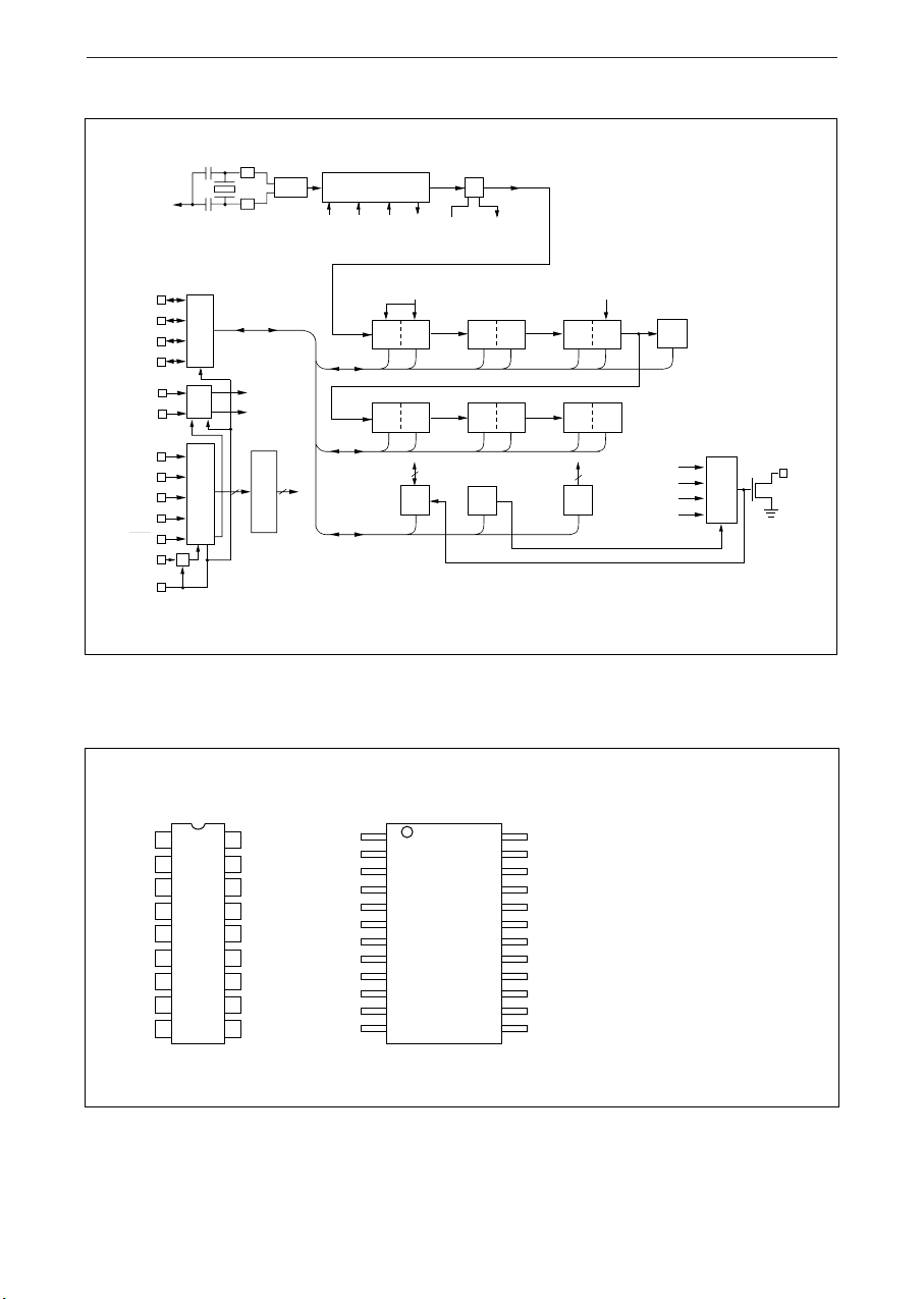
FUNCTIONAL BLOCK DIAGRAM
¡ SemiconductorMSM6242B
XT
32.768KHz
D
3
D
2
D
1
D
0
GATE
OSC
XT
WR
3
2
1
0
0
GATE
DECODER
GATE & LATCH
RD
A
A
A
A
CS
ALE
CS
1
PIN CONFIGURATION
COUNTER
30
STOP
RESET
bit
S
1
S
C
F
•
S
~W~Y10 are time counter register
1
C
•
0~CF
ADJ HOLD
bit
bit
30 sec
ADJ bit
S
S
10
1
D
D
10
1
C
D
are control register
1 Hz
BUSY
bit
bit
24/12bit
MI
MO
H
MI
1
10
MO
1
10
H
1
Y
Y
1
64Hz
W
10
10
STDP
1-sec carry
C
E
C
F
1-min carry
1-hour carry
STD.P
24
1
CS
2
0
3
ALE
4
A
0
5
A
1
A
6
2
A
7
3
8
RD
9
GND
18 pin Plastic DIP
STD.P
V
18
DD
17
XT
16
XT
15
CS
14
D
13
D
D
12
11
D
10
WR
CS
NC
ALE
1
0
1
2
3
NC
NC
RD
GND
1
2
0
3
4
5
A
0
6
A
7
1
8
A
9
2
A
10
3
11
12
24
23
22
21
20
19
18
17
16
15
14
13
V
XT
XT
NC
CS
D
NC
NC
D
D
D
WR
A
0-A3
DD
D
0-D3
CS
RD:
WR:
1
ALE:
0
STD.P:
XT, XT:
V
DD:
1
V
SS:
2
3
Data input/output
:
CHIP SELECTS 0,1
, CS1:
O
READ enable
WRITE enable
Address latch enable
Standard pulse output
XTAL oscillator input/output
+5V supply
ground
Address input
:
24 pin Plastic Small Outline
Package
Page 3
¡ Semiconductor MSM6242B
REGISTER TABLE
Address
Input
0
1
2
3
4
5
6
7
8
9
A
B
C
Address Input
A
A
3
0
0
0
0
0
0
0
0
1
1
1
1
1
A1A
2
0
0
0
0
0
1
0
1
1
0
1
0
1
1
1
1
0
0
0
0
0
1
0
1
1
0
0
0
1
0
1
0
1
0
1
0
1
0
1
0
Register
Name
S
1
S
10
MI
1
MI
10
H
1
H
10
D
1
D
10
MO
1
MO
10
Y
1
Y
10
W
D
mi
mo
y
Data
D
S
S
mi
mi
h
PM/
AM
d
mo
y
y
w
D
2
1
S
2
4
S
20
40
mi
2
4
mi
20
40
h
2
4
h
20
d
2
4
d
*
20
mo
2
4
*
*
y
2
4
y
20
40
w
2
4
3
S
8
*
8
*
h
8
*
d
8
*
8
*
y
8
80
*
D
S
mi
mi
h
d
mo
MO
y
Count
value
0
S
0 to 9
1
0 to 5
10
0 to 9
1
0 to 5
10
h
0 to 9
1
0 to 2
10
or 0 to 1
d
0 to 9
1
0 to 3
10
0 to 9
1
0 to 1
10
y
0 to 9
1
0 to 9
10
w
0 to 6
1
Description
1-second digit register
10-second digit register
1-minute digit register
10-minute digit register
1-hour digit register
PM/AM, 10-hour digit
register
1-day digit register
10-day digit register
1-month digit register
10-month digit register
1-year digit register
10-year digit register
Week register
1
1
0
D
1
E
F
1
1
1
1
1
0
1
1
REST = RESET
ITRPT/STND = INTERRUPT/STANDARD
Note 1)
Note 2)
Note 3)
Bit * does not exist (unrecognized during a write and held at "0" during a read).
Be sure to mask the AM/PM bit when processing 10's of hour's data.
BUSY bit is read only. The IRQ FLAG bit can only be set to a "0". Setting the IRQ FLAG to a "1" is done by
hardware.
Note 4)
PM at 1 and AM at 0 for PM / AM bit.
30
sec.
ADJ
t
1
TEST
IRQ
FLAG
t
0
24/12
C
D
C
E
C
F
Figure 1. Register Table
BUSY
ITRPT
/STND
STOP
HOLD
MASK
REST
—
—
—
Control Register D
Control Register E
Control Register F
25
Page 4
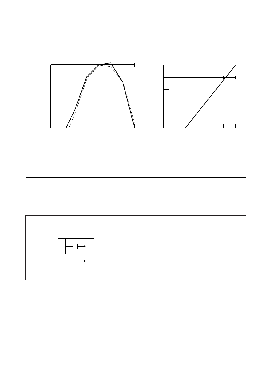
OSCILLATOR FREQUENCY DEVIATIONS
¡ SemiconductorMSM6242B
0
1
Ta = 25°C
0
-1
-50
∆f/f (PPM)
5V
-2
∆f/f (PPM)
-3
2V
-100
20 40 60 80
-60
-40 -20
0
Ta (°C)
Figure 2. Frequency Deviation (PPM) vs Temperature Figure 3. Frequency Deviation (PPM) vs Voltage
Note:
1. The graghs above showing frequency deviation vs temperature/voltage are primarily characteristic of the
-4
0
123456
V
(V)
DD
MSM6242B with the oscillation circuit described below.
XT
XT
Crystal: Type N0, P3 by kinseki (32.768 KHz)
C
G
C
D
V
DD
CG, CD: 22pF (Temperature Characteristics: 0)
26
Page 5
¡ Semiconductor MSM6242B
ABSOLUTE MAXIMUM RATINGS
Parameter Symbol Condition Rating
Power Supply Voltage
Input Voltage
Output Voltage
Storage Temperature
OPERATING CONDITIONS
Parameter Symbol Condition Rating
Power Supply Voltage
Standby Supply Voltage
Crystal Frequency
Operating Temperature
D.C. Characteristics
Parameter
"H" Input Voltage
"L" Input Voltage
Symbol
VIH1
VIL1
Condition
Unit
V
DD
V
I
V
O
T
STG
Ta = 25°C
-0. 3 to 7
-0.3 to VDD +0.3
-0.3 to VDD +0.3
-55 to +150
V
V
V
°C
Unit
V
DD
—
4 to 6
V
V
f
T
BAK
(XT)
OP
—
—
—
2 to 6
32.768
-40 to +85
kHz
°C
(VDD = 5V ± 10%, TA = -40 ~ +85)
Min.
—
—
2.2
—
Typ.
—
—
Max.
—
0.8
Unit
Applicable
All input termin-
V
als except CS1, XT
Terminal
Input Leak Current
Input Leak Current
"L" Output Voltage
"H" Output Voltage
"L" Output Voltage
OFF Leak Current
Input Capacitance
Current Consumption
Current Consumption
"H" Input Voltage
"L" Input Voltage
ILK1
ILK2
VOL1
V
VOL2
I
OFFLK
C
IDD1
IDD2
V
VIL2
OH
I
2
IH
VI = VDD/0V
IOL = 2.5mA
IOH = -400µA
IOL = 2.5mA
V = VDD/0V
Input frequency
1MHz
=
DD =
~
~
2 ~ 5.5V
VDD =
5V
VDD =
2V
f
(xt)
32.768
KHz
CS1 0
V
2.4
4/5V
Input terminals
—
—
1/-1
µA
—
—
—
—
—
—
—
—
—
—
5
——
10/-10
0.4
—
0.4
10
—
30
µA
PF
µA
—
DD
—
—
—
—
1/5V
10
—
DD
other than
D0 ~ D3, XT
D0 ~ D
3
V
D0 ~ D
3
V
STD.P
All input
terminals
V
DD
V
CS
1
27
Page 6
,,,,,,,,,,,
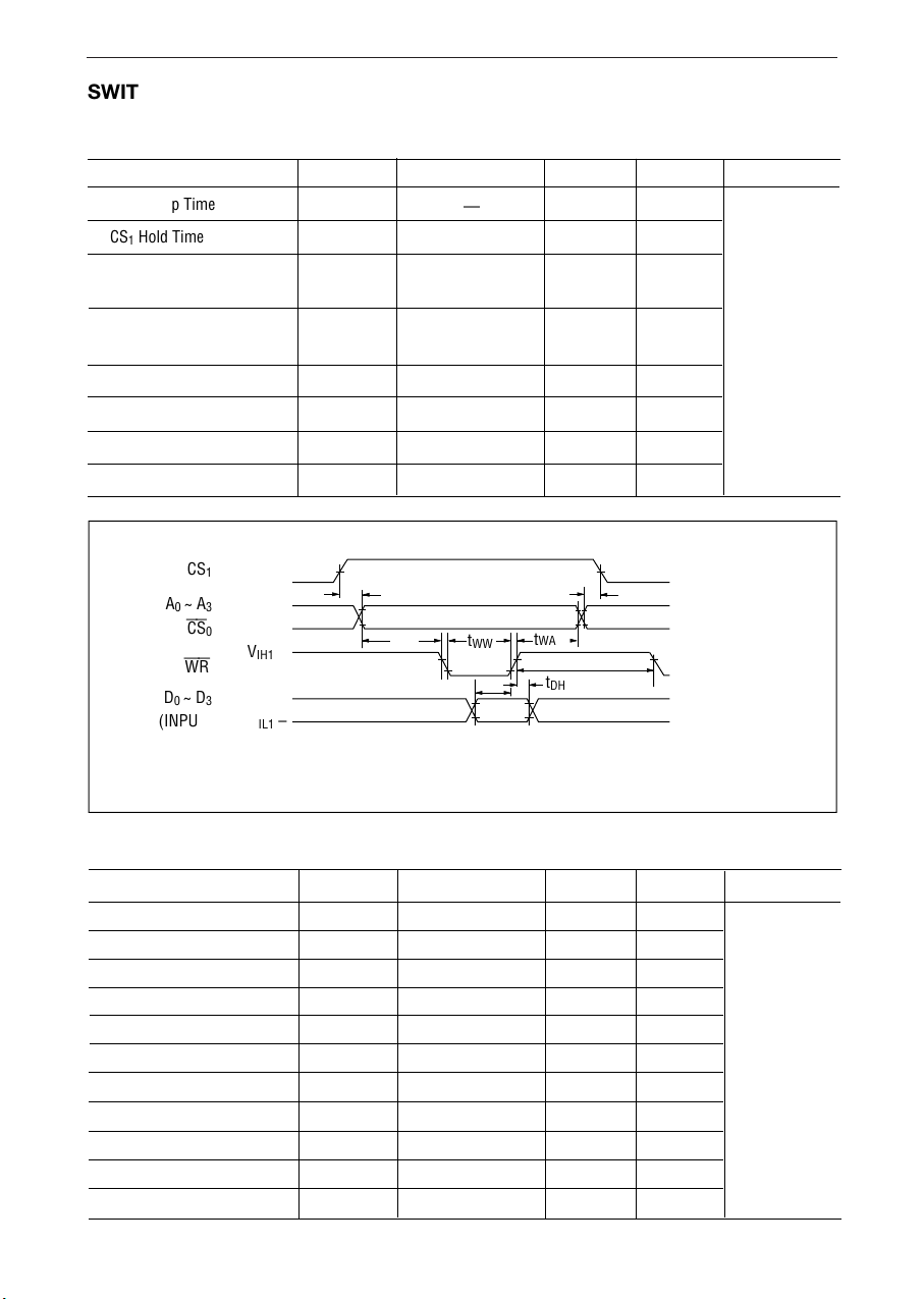
SWITCHING CHARACTERISTICS
(1) WRITE mode (ALE = VDD)
Parameter Symbol Condition Min.
CS1 Set up Time
CS1 Hold Time
Address Stable Before
WRITE
Address Stable After
WRITE
WRITE Pulse Width
Data Set up Time
Data Hold Time
RD / WR Recovery Time
t
t
t
t
t
t
WW
t
t
RCV
C1S
C1H
AW
WA
DS
DH
¡ SemiconductorMSM6242B
(VDD = 5V ± 10% Ta = -40 to +85°C)
Max.
—
—
—
—
—
—
—
—
1000
1000
20
10
120
100
10
60
—
—
—
—
—
—
—
—
Unit
ns
CS
A0 ~ A
CS
WR
D0 ~ D
(INPUT)
V
1
3
0
3
–
IH2
–
V
IH1
V
–
IL1
V
–
IH1
V
–
IH1
–
V
IL1
(2) WRITE mode (With use of ALE)
Parameter Symbol Condition Min.
CS1 Set up Time
Address Set up Time
Address Hold Time
ALE Pulse Width
ALE Before WRITE
WRITE Pulse Width
ALE After WRITE
DATA Set up Time
DATA Hold Time
CS1 Hold Time
RD / WR Recovery Time
t
C1S
t
AW
t
WW
t
DS
t
WA
t
RCV
t
DH
Figure 4. Write Cycle — (ALE = VDD)
t
C1S
t
AS
t
AH
t
AW
t
ALW
t
WW
t
WAL
t
DS
t
DH
t
C1H
t
RCV
—
—
—
—
—
—
—
—
—
—
—
1000
120
100
1000
t
C1H
V
= 2.2V
IH1
V
= 0.8V
IL1
V
= 4/5V
IH2
V
= 1/5V
IL2
(VDD = 5V ± 10%, Ta = -40 ~ +85°C)
Max.
—
25
25
40
10
20
10
60
—
—
—
—
—
—
—
—
—
—
Unit
DD
DD
ns
28
Page 7

¡ Semiconductor MSM6242B
,,,,
,,
,,,,,,,,,,,,,,,
,,,,,,,,
t
t
t
C1S
C1H
t
t
t
RD
t
DR
RCV
C1S
t
AS
t
AH
t
AW
t
ALW
t
WW
t
DS
t
WAL
t
t
C1H
V
= 2.2V
IH1
V
= 0.8V
IL1
V
= 4/5V
IH2
V
t
RCV
DH
IL2
= 1/5V
DD
DD
(VDD = 5V ± 10%, Ta = -40 to +85°C)
Max.
—t
—
AR
—
1000
1000
20
—
—
—
Unit
ns
RA
—
CL = 150pF
—
—
0
—
0
60
—
120
—
—
V
CS
A0 ~ A
CS
ALE
WR
D0 ~ D
(INPUT)
1
3
0
3
–
IH2
–
V
IH1
V
–
IL1
V
–
IH1
V
–
IL1
V
–
IH1
–
V
IL1
–
V
IH1
–
V
IL1
Figure 5. Write Cycle — (With Use of ALE)
(3) READ mode (ALE = VDD)
Parameter Symbol Condition Min.
CS1 Set up Time
CS1 Hold Time
Address Stable before
READ
Address Stable after
READ
RD to Data
Data Hold
RD / WR Recovery Time
CS
A0 ~ A
CS
RD
~ D
D
0
(OUTPUT)
V
–
IH2
1
t
C1S
–
V
3
IH1
V
–
IL1
0
V
–
IH1
V
–
IL1
VOH –
3
–
V
OL
t
AR
t
RD
t
RA
t
DR
t
RCV
t
C1H
V
V
V
V
IH1
IL1
IH2
IL2
= 2.2V
= 0.8V
= 4/5V
= 1/5V
DD
DD
VOH = 2.2V
VOL = 0.8V
"Z"
Figure 6. Read Cycle — (ALE = VDD)
29
Page 8

(4) READ mode (With use of ALE)
,,
,,,,,,,,,,,,,,,,
Parameter Symbol Condition Min.
¡ SemiconductorMSM6242B
(VDD = 5V ± 10%, Ta = -40 to +85°C)
Max.
Unit
Set up Time
CS
1
Address Set up Time
Address Hold Time
ALE Pulse Width
ALE before READ
ALE after READ
RD to Data
DATA Hold
Hold Time
CS
1
RD / WR Recovery Time
CS
1
A0 ~ A
3
CS
0
ALE
RD
D0 ~ D
3
(OUTPUT)
C1S
t
AS
t
AH
t
AW
t
ALR
t
RAL
t
RD
t
DR
t
C1H
t
RCV
V
–
IH2
t
C1S
–
V
IH1
V
–
IL1
V
–
IH1
V
–
IL1
V
–
IH1
–
V
IL1
–
V
OH
–
V
OL
t
AS
t
AW
—t
—
—
—
—
—
= 150pF
C
L
—
—
——
t
AH
t
ALR
t
RD
1000
25
25
40
10
10
—
0
1000
60
t
C1H
t
RAL
t
RCV
t
DR
120
" Z "
—
—
—
—
—
—
—
—
= 2.2V
V
IH1
V
= 0.8V
IL1
V
= 4/5V
IH2
V
= 1/5V
IL2
VOH = 2.2V
VOL = 0.8V
ns
DD
DD
Figure 7. Read Cycle — (With Use of ALE)
30
Page 9

¡ Semiconductor MSM6242B
PIN DESCRIPTION
Name
D
0
D
1
D
2
D
3
A
0
A
1
A
2
A
3
ALE
WR
RD
CS
0
CS
1
STD.P
Pin No.
14
13
12
11
4
5
6
7
3
10
8
2
15
1
GSRS
13
19
16
15
14
10
11
20
Description
Data Input/Output pins to be directly connected to a microcontroller bus for
reading and writing of the clock/calendar's registers and control registers. D0 = LSB
and D3 = MSB.
5
Address input pin for use by a microcomputer to select internal clock/calendar's
7
registers and control registers for Read/Write operations (See Function Table
Figure 1). Address input pins A0-A3 are used in combination with ALE for
9
addressing registers.
Address Latch Enable pin. This pin enables writing of address data when ALE = 1
and CSO = 0; address data is latched when ALE = 0 Microcontroller/Micro-
4
processors having an ALE output should connect to this pin; otherwise it should
be connected at V
DD
Writing of data is performed by this pin.
When CS
= 1 and CSO = 0, D0 ~ D3 data is written into the register at the rising
1
edge of WR.
Reading of register data is accomplished using this pin. When CS
and RD = 0, the data of this register is output to D
~ D3. If both RD and WR are
0
set at 0 simaltaneously, RD is to be inhibited.
2
Chip Select pins. These pins enable/disable ALE, RD and WR operation. CS
and ALE work in combination with one another, while CS1 work independent
with ALE. CS
must be connected to power failure detection as shown in Figure
1
18.
Output pin of N-CH OPEN DRAIN type. The output data is controlled by the
1
D
data content of CE register. This pin has a priority to CSO and CS1.
1
Refer to Figure 9 and FUNCTIONAL DESCRIPTION OF REGISTERS.
= 1, CSO = 0
1
O
XT
XT
V
DD
GND
16
17
18
22
32.768 kHz crystal is to be connected to these pins.
When an external clock of 32.768 kHz is to be used for MSM6242's oscillation
23
24
9
12
source, either CMOS output or pull-up TTL output is to be input from XT, while
XT should be left open.
Power supply pin. +2 ~ +6V power is to be applied to this pin.
Ground pin.
R
5M
Ω
FB
XT
X'tal
C
1
OR GND
V
DD
= C2 = 15 ~ 30pF
C
1
The impedance of the crystal should be less than 30k
32.768 kHz
C
XT
2
Figure 8. Oscillator Circuit Figure 9.
Ω
V
DD
STD.P OUTPUT
N-CH
31
Page 10

¡ SemiconductorMSM6242B
FUNCTIONAL DESCRIPTION OF REGISTERS
S1, S10, MI1, MI10, H1, H10, D1, D10, MO1, MO10, Y1, Y10, W
a) These are abbreviations for SECOND1, SECOND10, MINUTE1, MINUTE10, HOUR1,
HOUR10, DAY1, DAY10, MONTH1, MONTH10, YEAR1, YEAR10, and WEEK. These
values are in BCD notation.
b) All registers are logically positive. For example, (S8, S4, S2, S1) = 1001 which means 9
seconds.
c) If data is written which is out of the clock register data limits, it can result in erroneous clock
data being read back.
d) PM/AM, h20, h
In the mode setting of 24-hour mode, PM/AM bit is ignored, while in the setting of 12-hour
mode h20 is to be set. Otherwise it causes a discrepancy. In reading out the PM/AM bit in
the 24-hour mode, it is continuously read out as 0. In reading out h20 bit in the 12-hour mode,
0 is written into this bit first, then it is continuously read out as 0 unless 1 is being written
into this bit.
e) Registers Y1, Y10, and Leap Year. The MSM6242B is designed exclusively for the Christian
Era and is capable of identifying a leap year automatically. The result of the setting of a nonexistant day of the month is shown in the following example: If the date February 29 or
November 31, 1985, was written, it would be changed automatically to March 1, or
December 1, 1985 at the exact time at which a carry pulse occurs for the day's digit.
f) The Register W data limits are 0 – 6 (Tabel 1 shows a possible data definition).
10
TABLE 1
w
4
0
0
0
0
1
1
1
Using HOLD Bit Not Using HOLD Bit
HOLD Bit ← 1
Read BUSY Bit
Busy Bit= O?
YES
Write data into
or Read data from
~ W
registers S
1
HOLD Bit ← 0
NO
HOLD Bit
Idling Time
w
2
0
0
1
1
0
0
1
*
←
0
In the inside of LSI, the CLEAR of BUSY bit is performed when
*
HOLD bit = 0, but, if the period of HOLD bit =0 is extermely
narrow as compared with the period of HOLD bit = 1, there is
some case that the CLEAR of BUSY bit delays so that the
BUSY bit can be cleared by sampling HOLD bit = 0 at approximate
16KHz. It is recommended to allow an idling time of 62
w
1
0
1
0
1
0
1
0
Day of Week
ms or more.
Sunday
Monday
Tuesday
Wednesday
Thursday
Friday
Saturday
DATA
DATA1 = DATA2
DATA1 = DATA2
Read Register
S
~ W
1
Data of
←
S
1
Register
Read Register
~ W
S
1
YES
Figure 10. Reading and Writing of Registers S1 ~ W
First
~ W
Second
NO
32
Page 11

¡ Semiconductor MSM6242B
Reading Method 2 when Not Using HOLD Bit
*1
t
1
t0 *2
See Note
below
ITRPT/STNT 1
MASK
IRQ FLAG
TIME DATA READ
REGISTER CD READ
IRQ FLAG = 0
0
0
WAIT t
NO
(Note)
YES
Normal read
Initialization only at power ON
*1 and *2 represent the minimum required
•
time out.
For example
t1 = 0 and tO = 1 when required to a
unit of second;
= 1 and tO = 0 when required to a
t
1
unit of minute; and
= 1 and tO = 1 when required to a
t
1
unit of hour;
Retried the reading, since a
carry occurred during the
operation.
Do this process within the following
time requirements by combination
and t0:
between t
1
= 0 and tO = 1 . . . Less than 1 second
t
1
= 1 and tO = 0 . . . Less than 1 minute
t
1
= 1 and tO = 1 . . . Less than 1 hour
t
1
t : 12 HOUR MODE . . . 35µS
24 HOUR MODE . . . 3µS
Reading Method 3 when Not Using HOLD Bit
Initialization only at power ON
*1 and *2 represent the minimum required
•
*1
t
1
t0 *2
ITRPT/STNT 1
MASK
REGISTER CD READ
IRQ FLAG = 1
WAIT t
TIME DATA READ
IRQ FLAG
END
time unit.
0
CPU senses the
interruption.
NO
YES
0
For example
t
= 0 and tO = 1 when required to a
1
unit of second;
= 1 and tO = 0 when required to a
t
1
unit of minute; and
= 1 and tO = 1 when required to a
t
1
unit of hour;
The other IC causes
the interruption.
The interruption is caused by
this IC due to the occurrence
of a carry.
The IRQ FLAG is cleared to
read the next time data.
CD REGISTER (Control D Register)
a) HOLD (D0) – Setting this bit to a "1" inhibits the 1Hz clock to the S1 counter, at which
time the Busy status bit can be read. When Busy = 0, register's S1 ~ W
can be read or written. During this procedure if a carry occurs the S1
counter will be incremented by 1 second after HOLD = 0 (this condition
is guaranteed as long as HOLD = 1 does not exceed 1 second in
duration). If CS1 = 0 then HOLD = 0 irrespective of any condition.
b) BUSY (D1) – Status bit which shows the interface condition with microcontroller/
microprocessors. As for the method of writing into and reading from
S
~ W (address φ ~ C), refer to the flow chart described in Figure 10.
c) IRQ FLAG (D2) – This status bit corresponds to the output level of the STD.P output.
1
When STD.P = 0, then IRQ = 1; when STD.P = 1, then IRQ = 0. The IRQ
FLAG indicates that an interrupt has occurred to the microcomputer if
IRQ = 1. When D0 of register CE (MASK) = 0, then the STD.P output
changes according to the timing set by D3 (t1) and D2 (t0) of register E.
When D1 of register E (ITRPT/STND) = 1 (interrupt mode), the STD.P
output remains low until the IRQ FLAG is written to a "0". When IRQ
= 1 and timing for a new interrupt occurs, the new interrupt is ignored.
When ITRPT/STND = 0 (Standard Pulse Output mode) the STD.P
output remains low until either "0" is written to the IRQ FLAG;
otherwise, the IRQ FLAG automatically goes to "0" after 7.8125ms.
When writing the HOLD or 30 second adjust bits of register D, it is
necessary to write the IRQ FLAG bit to a "1".
d) ±30 ADJ (D3) – When 30-second adjustment is necessary, a "1" is written to bit D3
during which time the internal clock registers should not be read from
or written to 125µs after bit D3 = 1 it will automatically return to a "0",
and at that time reading or writing of registers can occur.
33
Page 12

¡ SemiconductorMSM6242B
START
30-SECOND
ADJ BIT = 1
READ 30-SECOND
ADJ BIT
30-SECOND
ADJ BIT = 0?
YES
END
(A)
NO
START
30-SECOND
ADJ BIT = 1
125µs PASS?
YES
END
(B)
NO
Figure 11. Writing 30-Second Adj. bit (Two Ways A, B)
CE REGISTER (Control E Register)
a) MASK (D0) – This bit controls the STD.P output. When MASK = 1, then STD.P
= 1 (open); when MASK = 0, then STD.P = output mode. The
relationship between the MASK bit and STD.P output is shown
Figure 12.
b) ITRPT/STND (D1) – The ITRPT/STND input is used to switch the STD.P output
between its two modes of operation, interrupt and Standard
timing waveforms. When ITRPT/STND = 0 a fixed cycle waveform with a low-level pulse width of 7.8125ms is present at the
STD.P output. At this time the MASK bit must equal 0, while the
period in either mode is determined by T0 (D2) and T1 (D3) of
Register E.
c) T0 (D2), T1 (D3) – These two bits determine the period of the STD.P output in both
interrupt and Fixed timing waveform modes. The tables below
show the timing associated with the T0, T1 inputs as well as their
relationship to INTRPT/STND and STD.P.
MASK BIT
STD.P OUTPUT
34
t
1
0
0
1
1
"1" "1"
"0" "0"
t
0
0
1
0
1
"INTERRUPT" DOES
NOT OCCUR BECAUSE
MASK BIT IS "1"
OPEN
LOW LEVEL
WRITE "0" INTO IRQ FLAG BIT
"INTERRUPT" TIMING
Period
1/64 second
1 second
1 minute
1 hour
MASK BIT
STD.P
OUTPUT
Figure 12.
TABLE 2
"1" "1"
"0" "0"
INTRT/STND BIT = "0"INTRT/STND BIT = "1"
Duty CYCLE of "0" level when
ITRPT/STND bit is "0".
1/2
1/128
1/7680
1/460800
OUTPUT DOES NOT OCCUR
AT LOW LEVEL BECAUSE
MASK BIT IS "1"
OPEN
LOW LEVEL
OUTPUT TIMING
AUTOMATIC RETURN
Page 13

¡ Semiconductor MSM6242B
The timing of the STD.P output designated by T1 and T0 occurs the moment that a carry occurs to a clock digit.
(EXAMPLE) WHEN t1 = 1, t0 = 1 and MASK = 0.
PM12:00
PM1:00
WHEN ITRPT/STND
BIT is "1"
STD.P OUTPUT
WHEN ITRPT/STND
BIT is "0"
OPEN
LOW LEVEL
OPEN
LOW LEVEL
d) The low-level pulse width of the fixed cycle waveform (ITRPT/STND = 0) is 7.8125ms
independent of T0/T1 inputs.
e) The fixed cycle waveform mode can be used for adjustment of the oscillator frequency time
base. (See Figure 14).
f) During ±30 second adjustment a carry can occur that will cause the STD.P output to go low
when T0/T1 = 1,0 or 1,1. However, when T1/T0 = 0, 0 and ITRPT/STND = 0, carry does
not occur and the STD.P output resumes normal operation.
g) The STD.P output is held (frozen) at the point at which STOP = 1 while ITRPT/STND = 0.
h) No STD.P output change occurs as a result of writing data to registers S1 ~ H1.
CF REGISTER (Control F Register)
a) REST (D0) – This bit is used to clear the clock's internal divider/counter of less than a
"RESET" second. When REST = 1, the counter is Reset for the duration of REST. In
order to release this counter from Reset, a "0" must be written to the REST
bit. If CSI = 0 then REST = 0 automatically.
b) STOP (D1) – The STOP FLAG Only inhibits carries into the 8192Hz divider stage.
There may be up to 122µs delay before timing starts or stops after
changing this flag; 1 = STOP/0 = RUN.
STOP BIT
"1"
"0"
"1" "1"
"0" "0" "0"
TIMING OF
"CARRY"
TO 8192Hz
"CARRY" EXECUTED
"CARRY" NOT EXECUTED
Figure 13
c) 24/12 (D2) – This bit is for selection of 24/12 hour time modes. If D2 = 1–24 hour mode
is selected and the PM/AM bit is invalid. If D2 = 0–12 hour mode is
selected and the PM/AM bit is valid.
"24/HOUR/ Setting of the 24/12 hour bit is as follows:
12 HOUR" 1) REST bit = 1
2) 24/12 hour bit = 0 or 1
3) REST bit = 0
* REST bit must = 1 to write to the 24/12 hour bit.
d) TEST (D3) – When the TEST flag is a "1", the input to the SECONDS counter comes
from the counter/divider stage instead of the 15th divider stage. This
makes the SECONDS counter count at 5.4163KHz instead of 1Hz. When
TEST = 1 (Test Mode) the STOP & REST (Reset) flags do not inhibit internal
counting. When Hold = 1 during Test (Test = 1) internal counting is
inhibited; however, when the HOLD FLAG goes inactive (Hold = 0)
counter updating is not guaranteed.
35
Page 14

¡ SemiconductorMSM6242B
TYPICAL APPLICATION INTERFACE WITH MSM6242B AND
MICROCONTROLLERS
8085
AD
3
AD
2
AD
1
AD
0
A8 ~ A
15
S
1
S
0
IO/M
DECODER
ALE
RD
WR
MEMORY MAPPED
Z80
D
3
D
2
D
1
D
0
A
3
A
2
A
1
A
0
DECODER
~ A
A
4
15
IORQ
MREQ
RD
WR
Note : It depends upon the switching
characterisrics decided by a X'tal used
for a Z80 that either of IORQ and MREQ
is used.
Figure 16.
R
1
R
2
MSM6242B
D
3
D
2
D
1
D
0
A
3
A
2
A
1
A
0
CS
0
ALE
RD
WR
8085
A8 ~ A
~ A
A
8
IO/M
A/D
RD
WR
12
15
S
1
S
0
DECODER
I/O MAPPED
Note : If 8085 does not enter into the state of HALT or HOLD during CS1 = "H" of
are not required
MSM6242B, R
1
and R
2
.
Figure 15.
G1
G2
V
DD
MSM6242B
D
3
D
2
D
1
D
0
A
3
A
2
A
1
A
0
CS
0
ALE
RD
WR
MCS48
BUS
BUS
BUS
BUS
BUS 4-7
ALE
RD
WR
3
2
1
0
DECODER
Figure 17.
R
1
R
2
MSM6242B
D
3
D
2
D
1
D
0
A
3
A
2
A
1
A
0
CS
0
ALE
RD
WR
MSM6242B
D
3
D
2
D
1
D
0
A
3
A
2
A
1
A
0
CS
0
ALE
RD
WR
36
Page 15

¡ Semiconductor MSM6242B
TYPICAL APPLICATIONS — INTERFACE WITH MSM80C49
100µf
3.9V
22pf
4.553 KHz
22pf
40
38
2
3
1
X
1
X
2
80C49RS
V
CC
T
0
P
27
V
DD
MSM
V
SS
20
★
LITHIUM
BATTERY
★
26
6
INT
11
ALE
8
RD
10
WR
18K
V
1
SDT.P
3
ALE
8
RD
10
WR
MSM
6242BRS
TR1
4/14
5/13
6/12
7/11
2
15
10K
A/D
A/D
A/D
A/D
CS
CS
0
1
2
3
0
1
DB
DB
DB
DB
DB
P
12
0
13
1
14
2
15
3
19
7
34
17
820
4.7µf (tantalum)
★
(VFWD = < 0.3V)
i.e. GERMANIUM
DIODE
18
DD
17
XT
16
XT
9
V
SS
15pf
32.768 KHz
5-35pf
RS232
DB25
CONNECTOR
1.8K
220
TR2
★
1.8K 1.8K
★
10µf
1.8K
2
3
7
5
20
220
1.8K
TR3
RS232
TR1 = 2N2907
TR2 = 2N2907
TR3 = 2N2222
★ = 1N4148
INTERFACE
5.2V
Figure 18.
37
Page 16

APPLICATION NOTE
1. Power Supply
START
¡ SemiconductorMSM6242B
= 5V
V
DD
2. Adjustment of Frequency
V
DD
16
XT XT
= (t1, t0, 0, 0)
3
V
DD
18 17
V
DD
CD, CF = (0, 0, 0, 0)
C
E
SDT.P
12
Power On
TEST Bit ← 0
REST Bit ← 0
24/12 Bit ← 1*
STOP Bit ← 1
REST Bit ← 0
24/12 Bit ← 2*
Set the current
time
HOLD Bit ← 0
STOP Bit ← 0
Start Operation
Screwdriver
STD.P
Output = undifined
1* = 2*
(1 or 0)
d
c
Frequency
counter
C
~ CF are to be set at as described in the
D
figure and the capacitor is to be adjusted
to meet the settle frequency of t
If the right oscillation can not be obtained,
1. Check the waveform of XT
2. Check C
3. Check the noise
~ CF content
D
38
Eye
and t1.
0
1
b
0.1 INCH
: INHIBIT
≥ 0.3 INCH
1
≥ 0.2 INCH
2
b
2
XT XT
V
DD
a
a
Page 17

¡ Semiconductor MSM6242B
3. CH1 (Chip Select)
VIH and VIL of CH1 has 3 functions.
a) To accomplish the interface with a microcontroller/microprocessor.
b) To inhibit the control bus, data bus and address bus and to reduce input gate pass
current in the stand-by mode.
c) To protect internal data when the mode is moved to and from standby mode.
To realize the above functions:
a) More than 4/5 VDD shoud be applied to the MSM6242B for the interface with a
microcontroller/microprocessor in 5V operation.
b) In moving to the standby mode, 1/5 VDD should be applied so that all data buses should
be disabled. In the standby mode, approx. 0V should be applied.
c) To and from the standby mode, obey following Timing chart.
To Standby Mode
V
DD
CS
1
CS0 : H
or WR : H
4. Set SDT.P at alarm mode
10
YES
and
1
5
D
4 ~ 6V
2 ~ 4V
V
DD
NO
Start interruption
CPU Activation
4V 4V
2µs (MIN)
2
V
DD
5
Set alarm at 9:00
MASK BIT ← 0
ITRPT/STND BIT ← 1
t
, t0 ← 1
1
Read Register C
D2 = 1?
Read H
H
Cotent
10
From Standby Mode
2µs (MIN)
4
V
5
Repeat
DD
AM 9:00?
YES
NO
CPU HALT
or
CPU STAND BY
39
Page 18

TYPICAL APPLICATION — POWER SUPPLY CIRCUIT
RIPPLE
OPERATING: 20mV P-P
BATTERY BACKUP: 0mV
22µf
100Ω
1.2 x 3 = 3.6V
Ni – Cd
4.7µf
V
DD
MSM
6242B
V
SS
+5V
RL
RL
+5V
VCE (SAT.) = 0.1V
10K
51K
10K
M
C
B
1.5 x 2 = 3V
DRY CELLS
¡ SemiconductorMSM6242B
100Ω
4.7µf
V
DD
MSM
6242B
V
SS
Figure 19.
V
DD
MSM
6242B
V
SS
4.7µf
Figure 21.
100Ω
RL
1.2 x 3 = 3.6V
Ni – Cd
220Ω
Figure 20.
~
6.5V
~
D
1
+5V
4.7µF: tantalum
SUPPLEMENTARY DESCRIPTION
• When "0" is written to the IRQ FLAG bit, the IRQ FLAG bit is cleared. However, if "0" is
assigned to the IRQ FLAG bit when written to the other bits, the 30-sec ADJ bit and the
HOLD bit, the IRQ FLAG = 1 and was generated before the writing and IRQ FLG = 1
generated in a moment then will be cleared. To avoid this, always set "1" to the IRQ
FLAG unless "0" is written to it intentionally. By writing "1" to it, the IRQ FLAG bit
does not become "1".
• Since the IRQ FLAG bit becomes "1" in some cases when rewriting either of the t1, t0, or
ITRPT/STND bit of register CE, be sure to write "0" to the IRQ FLAG bit after writing to
make valid the IRQ FLAG = 1 to be generated after it.
* The relationship between SDT.P OUT and IRQ FLAG bit is shown below:
40
STD.P OUT
IRQ FLAG bit
open
"L"
1
0
approx. 1.95 ms
 Loading...