

Page 1

E2B0022-27-Y2
¡ Semiconductor
¡ Semiconductor
This version: Nov. 1997
Previous version: Mar. 1996
MSM5839B
MSM5839B
40-DOT SEGMENT DRIVER
GENERAL DESCRIPTION
The MSM5839B is a dot matrix LCD segment driver LSI which is fabricated using low power
CMOS metal gate technology. This LSI consists of two 20-bit shift registers, two 20-bit latches,
a 40-bit level shifter and a 40-bit 4-level driver.
It converts serial data, which is received from an LCD controller LSI, to parallel data and outputs
LCD driving waveform to the LCD panel.
Expansion of display can easily be made by increasing the number of characters and character
patterns.
This LSI can drive a variety of LCD panels because the bias voltage, which determines the LCD
driving voltage, can be optionally supplied from the external source.
FEATURES
• Supply voltage : 4.5 to 5.5V
• LCD driving voltage : 8 to 18V
• Applicable LCD duty : 1/32 to 1/128
• Bias voltage can be supplied externally
• Applicable common driver : MSM5238 (32 outputs)
• Package options:
56-pin plastic QFP (QFP56-P-910-0.65-K) (Product name: MSM5839B GS-K)
56-pin plastic QFP (QFP56-P-910-0.65-L2) (Product name: MSM5839B GS-L2)
56-pin plastic QFP (QFP56-P-910-0.65-2K) (Product name: MSM5839B GS-2K)
1/11
Page 2
¡ Semiconductor
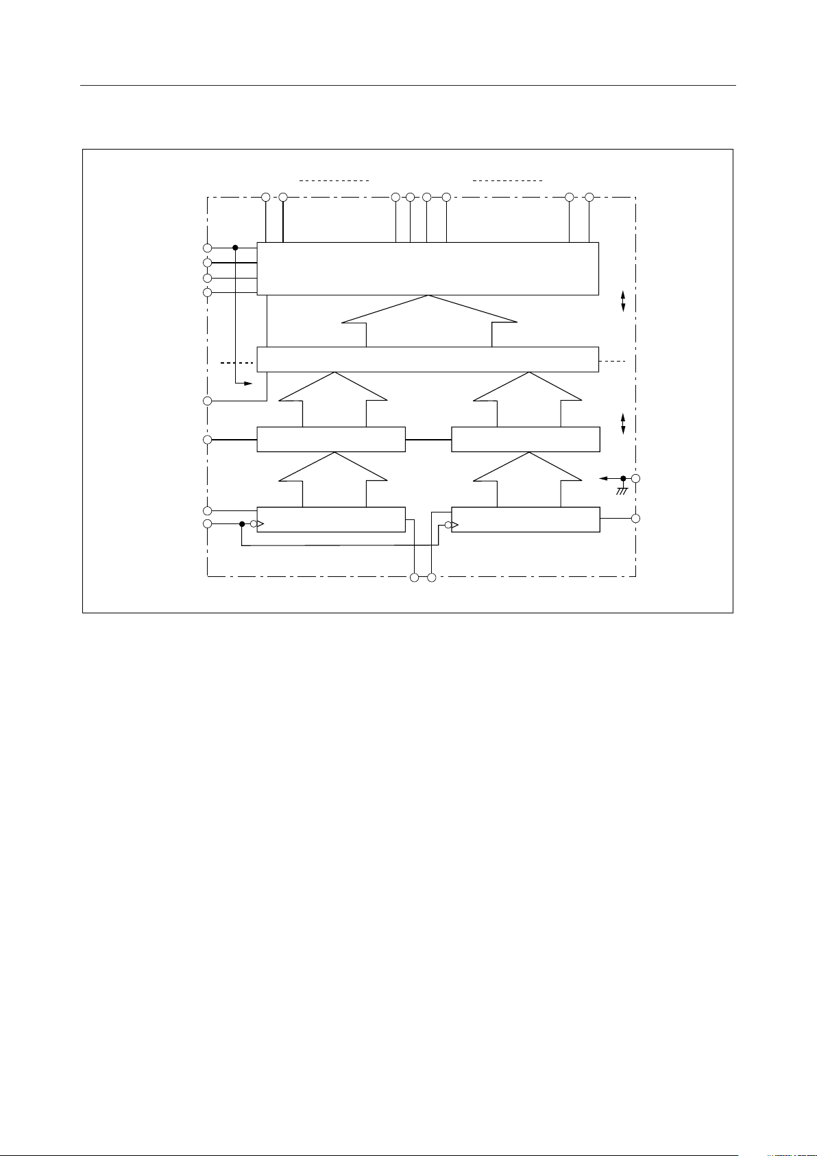
BLOCK DIAGRAM
MSM5839B
VDD(V1)
V
V
V
EE(V4
DF
LOAD
DI
CP
O1O
2
2
3
O19O20O21O
22
40-Bit 4-Level Driver
O39O
40
V
DD
)
V
EE
40-Bit Level Shifter
V
DD
20-Bit Latch 20-Bit Latch
1
20-Bit Shift
Register
20-Bit Shift
Register
V
SS
V
SS
DO
40
DO20DI
21
2/11
Page 3
¡ Semiconductor
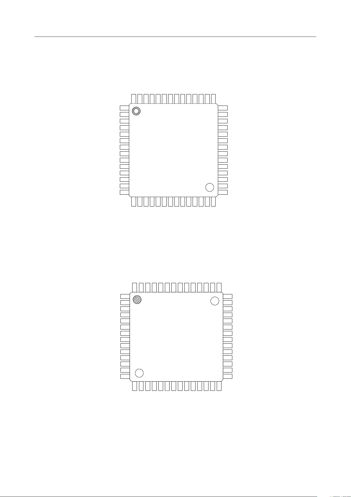
PIN CONFIGURATION
MSM5839B
(Top view)
)
1
(V
1
DI
20
O
CP
)
DD
V
VSSV
21
DD
O
O
LOAD
DF
NC
NC
NC
56555453525150494847464544
1
O
1
O
2
2
O
3
3
4
O
4
5
O
5
6
O
6
7
O
7
8
O
8
9
O
9
10
O
10
11
O
11
12
O
12
13
O
13
14
O
14
15161718192021222324252627
15
19
O18O17O16O
O
)
4
(V
20
EE
2
3
V
23
22
O24O
DI 21DO
V
43
42
DO
40
O
41
40
O
40
39
39
O
38
38
O
37
37
O
36
36
O
35
35
O
34
34
O
33
33
O
32
32
O
31
31
O
30
30
O
29
29
O
28
28
27O26
25
O
O
*(V
NC: No connection
NC
NC
NC
DF
LOAD
DI
CP
VDD(V1)
V
VEE(V4)
DO
DI
56-Pin Plastic QFP (Type K)
O1O2O3O4O5O6O7O8O9O10O11O12O13O
2
1
56
55
54
53
52
51
1
50
49
48
SS
47
V
2
V
46
3
45
44
20
43
21
42
40O40O39O38O37O36O35O34O33O32O31O30O29O28
4
3
56789
41
39
40
383736353433323130
DO
NC: No connection
1011121314
14
O
15
15
O
16
16
O
17
17
O
18
18
19
O
19
O
20
20
21
*(VDD)
22
O
21
23
O
22
24
O
23
O
25
24
O
26
25
O
27
26
O
28
27
29
56-Pin Plastic QFP (Type L)
* This pin is internally connected to VDD, so connect it to the power supply or leave it open.
Note : The figure for Type L shows the configuration viewed from the reverse side of the package.
Pay attention to the difference in pin arrangement.
3/11
Page 4
¡ Semiconductor
ABSOLUTE MAXIMUM RATINGS
Parameter Symbol Condition Rating Unit
Supply Voltage (1) V
Supply Voltage (2)
Input Voltage
Storage Temperature
DD
V
–
DD
V
–
DD
V
T
STG
MSM5839B
*1
*1
V
EE
2
*
V
EE
1
Ta = 25°C
Ta = 25°C
Ta = 25°C
Ta = 25°C
—
0.3 to +6
–
0 to 18
0 to 18
0.3 to V
–
55 to +150
–
DD
+0.3
V
V
V
V
°C
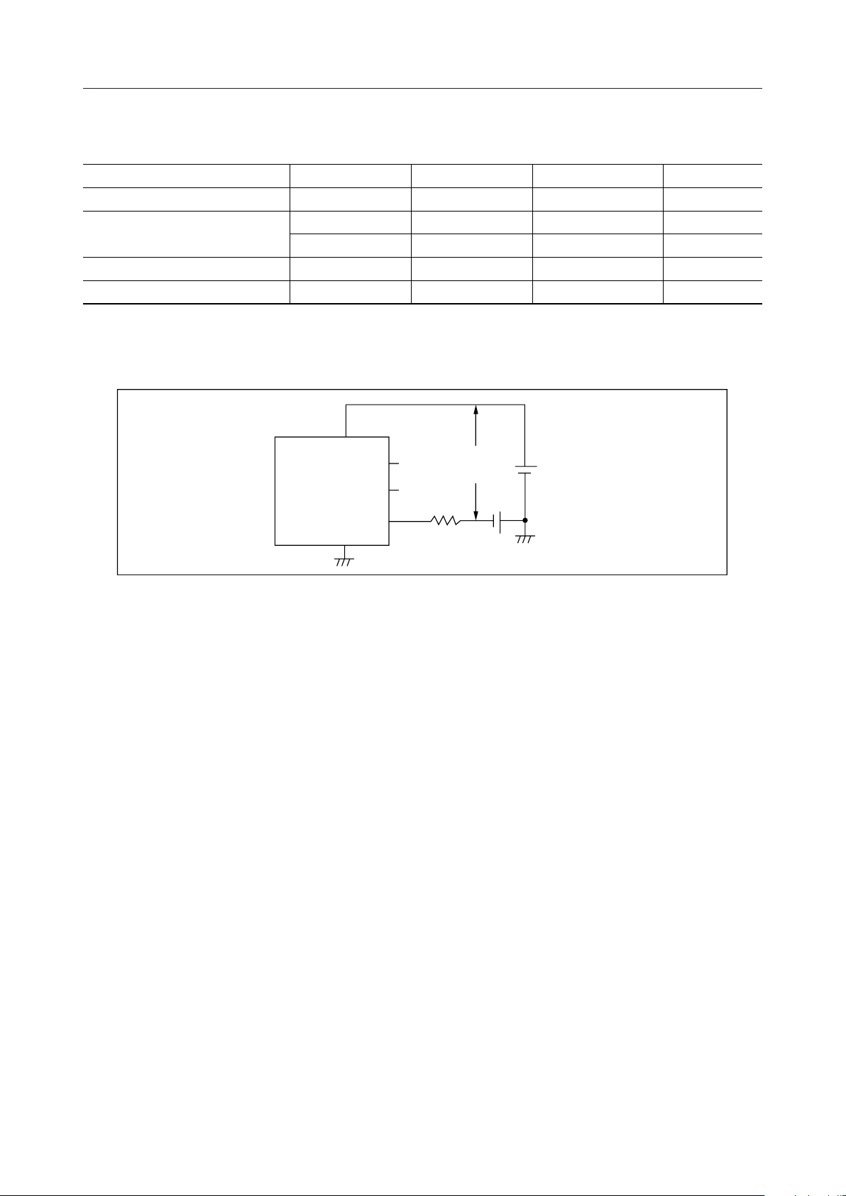
*1 VDD>V2>V3>V
EE
*2 Applies when a series resistor of 47W or more is connected as shown below.
V
DD
R
S
V
DD–VEE
>
47W
=
+V
–V
MSM5839B
V
SS
V
2
V
3
V
EE
4/11
Page 5

¡ Semiconductor
RECOMMENDED OPERATING CONDITIONS
Parameter Symbol Condition Range Unit
MSM5839B
Supply Voltage (1)
Supply Voltage (2)
Operating Temperature
*1 VDD>V2>V3>V
EE
V
DD
EE
EE
1
*
1
*
2
*
V
V
–
DD
V
V
–
DD
T
op
—
—
4.5 to 5.5
8 to 16
— 8 to 18 V
—
–20 to +85
*2 Applies when a series resistor of 47W or more is connected as shown below.
V
DD
R
≥ 47W
S
V
DD–VEE
+V
–V
MSM5839B
V
SS
V
2
V
3
V
EE
V
V
°C
ELECTRICAL CHARACTERISTICS
DC Characteristics
= 5V ±10%, Ta = –20 to +85°C)
(V
DD
SS
*3
Min.
0.8V
V
SS
Typ. Max.
DD
—V
— 0.2V
—— 1V
——–1V
VDD–0.4 — —I
— — 0.4
— 3.5 7
— — 100
DD
DD
Parameter
"H" Input Voltage
"L" Input Voltage
"H" Input Current
"L" Input Current
"H" Output Voltage
"L" Output Voltage V
ON Resistance kW
Supply Current
Symbol Condition
1
*
V
IH
1
*
V
IL
1
*
I
IH
1
*
I
IL
2
*
V
OH
2
V
*
OL
4
R
*
ON
O
I
V
DD–VEE
V
N–VO
—
—
= V
I
= 0V
I
=–0.4mA
= 0.4mA
O
= 0.25V
DD
= 10V
Connect all inputs to V
I
DD
VDD–V
= 18V, No load
EE
DD
or V
*1 Applicable to LOAD, CP, DI1, DI21, DF
*2 Applicable to DO20, DO
*3 VN = VDD to V
EE, V3
*4 Applicable to O1 - O
40
2
= (VDD–VEE), V2 = (VDD–VEE)
9
40
7
9
Unit
V
V
mA
mA
V
mA
5/11
Page 6

¡ Semiconductor
MSM5839B
Switching Characteristics
Parameter
"H", "L" Propagation Delay Time
Clock Frequency
Clock Pulse Width
LOAD Pulse Width
Data Setup Time DI Æ CP
LOAD Time
CP
Æ
Æ
CP Time
Æ
CP
LOAD
Data Hold Time DI
CP Rise/Fall Time ns
LOAD Rise/Fall Time ms
Symbol Condition
tp
LH
tp
HL
f
CP
t
(CP)
W
t
(L)
W
t
SETUP
t
CL
t
LC
t
HOLD
t
(CP)
r
t
(CP)
f
t
(L)
r
t
(L)
f
DUTY
(V
= 5V ±10%, Ta = –20 to +85°C, CL = 15pF)
DD
Min.
——
= 50%
—
—
—
—
—
—
—
—
—
125 — —
125 — —
50 — —
250 — —
0——
50 — —
——50
——1
Typ. Max.
— 250
—
3.3 MHz
Unit
ns
ns
ns
ns
ns
ns
ns
CP
DI
, DI
1
21
DO20, DO
LOAD
t
f(CP)
t
w(CP)
t
SETUP
0.8V
DD
0.8V
0.2V
0.8V
DD
0.2V
DD
0.8V
DD
40
0.2V
t
t
DD
DD
PLH
PHL
DD
t
w(CP)
t
HOLD
0.8V
0.2V
DD
DD
t
CL
0.8V
0.2V
DD
t
r(L)
DD
0.2V
t
w(L)
t
r(CP)
0.8V
DD
DD
0.8V
t
SETUP
DD
t
f(L)
0.8
V
DD
0.2
V
DD
t
LC
0.2V
0.8V
DD
DD
0.2V
0.8
V
0.2
V
DD
t
HOLD
DD
DD
6/11
Page 7

¡ Semiconductor
MSM5839B
FUNCTIONAL DESCRIPTION
Pin Functional Description
•DI
1
The data input pin for the 20-bit shift register (from 1st to 20th bit). The display data is input
to the data pin in synchronization with a clock pulse.
•CP
Clock pulse input pin for the two 20-bit shift registers. The data is shifted in the two 20-bit shift
registers at the falling edge of the clock pulse. Data setup time (t
(t
•DO
) are required each between DI1, DI21 and CP. Refer to the Switching Characteristics.
HOLD
20
The 20th output bit of the shift register.
The data which is input from DI1 is clocked out with the delay in the number of bits of the shift
register (20). A 40-bit shift register can be configured by connecting the output of this pin to
DI21 pin.
) and data hold time
SETUP
•DI
21
The data input pin for the 20-bit shift register (from 21st to 40th bit).
Connecting the DO20 pin and this pin allows the device to be used as a 40-bit shift register.
•DO
40
The 40th output bit of the shift register.
The data which is input from DI1 is clocked out with the delay in the number of the bits of the
shift register (20).
When extending the number of characters, this pin is used to cascade connect the next
MSM5839B.
•DF
Alternate signal input pin for LCD driving waveform.
•VDD(V1), V
SS
Supply voltage pins. VDD should be 4.5 to 5.5V.
VSS is the ground pin (VSS = 0V).
•V2, V3, VEE(V4)
Bias supply voltage pins to drive the LCD. Bias voltage is supplied from an external source.
• LOAD
The signal for latching the shift register contents is input from this pin.
When LOAD pin is set at "H", the shift register contents are transferred to the 40-bit 4-level
driver. When LOAD pin is set at "L", the last display output data (O1 to O40), which was
transferred when LOAD pin was at "H", is held.
7/11
Page 8

¡ Semiconductor
MSM5839B
•O1 to O
40
Display data output pins which correspond to each data bit in the latch.
One of VDD, V2, V3 or VEE (V4) is selected as a display driving voltage source based on the
combination of latched data level and DF signal. Refer to the Truth Table below.
These pins should be connected to the SEGMENT side of the LCD panel.
Truth Table
Latched data DF LCD driver output
H
HV
LV
HV
L
LV
)
EE (V4
)
DD (V1
3
2
8/11
Page 9

¡ Semiconductor
PACKAGE DIMENSIONS
QFP56-P-910-0.65-K
Mirror finish
MSM5839B
(Unit : mm)
Package material
Lead frame material
Pin treatment
Solder plate thickness
Package weight (g)
Epoxy resin
42 alloy
Solder plating
5 mm or more
0.36 TYP.
Notes for Mounting the Surface Mount Type Package
The SOP, QFP, TSOP, SOJ, QFJ (PLCC), SHP and BGA are surface mount type packages, which
are very susceptible to heat in reflow mounting and humidity absorbed in storage.
Therefore, before you perform reflow mounting, contact Oki’s responsible sales person for the
product name, package name, pin number, package code and desired mounting conditions
(reflow method, temperature and times).
9/11
Page 10

¡ Semiconductor
QFP56-P-910-0.65-L2
Spherical surface
MSM5839B
(Unit : mm)
Package material
Lead frame material
Pin treatment
Solder plate thickness
Package weight (g)
Epoxy resin
42 alloy
Solder plating
5 mm or more
0.36 TYP.
Notes for Mounting the Surface Mount Type Package
The SOP, QFP, TSOP, SOJ, QFJ (PLCC), SHP and BGA are surface mount type packages, which
are very susceptible to heat in reflow mounting and humidity absorbed in storage.
Therefore, before you perform reflow mounting, contact Oki’s responsible sales person for the
product name, package name, pin number, package code and desired mounting conditions
(reflow method, temperature and times).
10/11
Page 11

¡ Semiconductor
QFP56-P-910-0.65-2K
Mirror finish
MSM5839B
(Unit : mm)
Package material
Lead frame material
Pin treatment
Solder plate thickness
Package weight (g)
Epoxy resin
42 alloy
Solder plating
5 mm or more
0.43 TYP.
Notes for Mounting the Surface Mount Type Package
The SOP, QFP, TSOP, SOJ, QFJ (PLCC), SHP and BGA are surface mount type packages, which
are very susceptible to heat in reflow mounting and humidity absorbed in storage.
Therefore, before you perform reflow mounting, contact Oki’s responsible sales person for the
product name, package name, pin number, package code and desired mounting conditions
(reflow method, temperature and times).
11/11
 Loading...