

Page 1
¡ Semiconductor MSM58321
¡ Semiconductor
MSM58321
REAL TIME CLOCK/CALENDAR
DESCRIPTION
The MSM 58321 is a metal gate CMOS Real
Time Clock/Calendar with a battery backup
function for use in bus-oriented microprocessor applications.
The 4-bit bidirectional bus line method is used
for the data I/O circuit; the clock is set, corrected, or read by accessing the memory.
FEATURES
• 7 Function-Second, Minute, Hour, Day,
Day-of-Week, Month, Year
• Automatic leap year calender
• 12/24 hour format
• Frequency divider 5-poststage reset
• Reference signal output
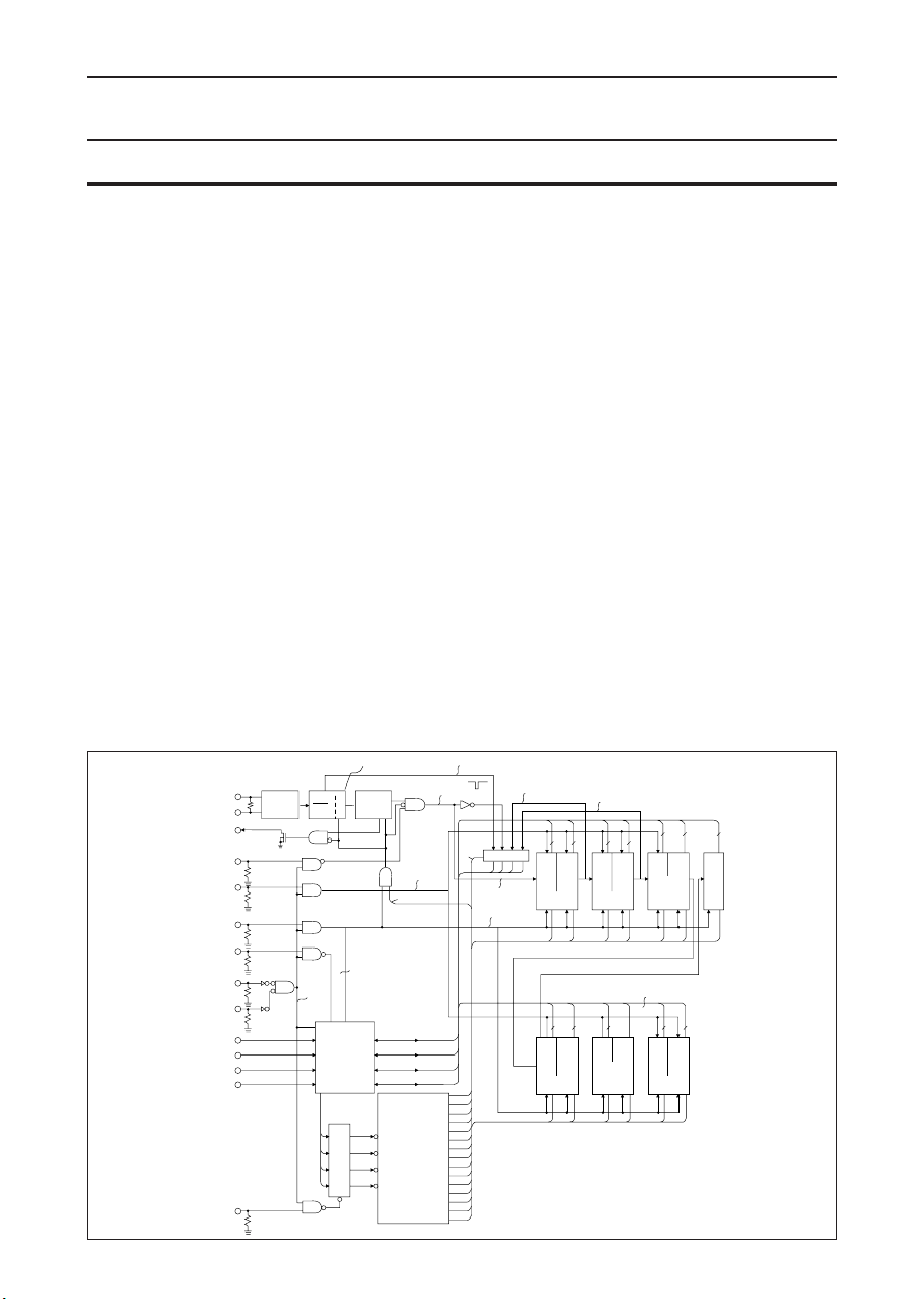
FUNCTIONAL BLOCK DIAGRAM
5-poststage (O
11~O15
RFB
XT
XT
BUSY
STOP
TEST
WRITE
READ
CS1
CS2
D0
D1
D2
D3
ADDRESS
WRITE
R
R
R
R
R
R
R
1
2
CS
15
WRIETE
TRI-STATE
CONTROL
ADDRESS
LATCH
BUSY
R
R
TEST
D
READ
ADDRESS
DECODER
OSC
N
p
p
p
p
p
p
p
The time is read with 4-bit DATA I/O, ADDRESS WRITE, READ, and BUSY; it is written
with 4-bit DATA I/O, ADDRESS WRITE,
WRITE, and BUSY.
• 32.768 kHz crystal controlled operation
• Single 5V power supply
• Back-up battery operation to VDD = 2.2V
• Low power dissipation
90 µW max. at VDD = 3V
2.5 mW max. at VDD = 5V
• 16 pin plastic DIP (DIP 16-P-300)
)
1024 Hz
1 Hz
E-F
S1
0
S10
1
MI1
2
MI10
3
H1
4
H10
5
W
6
D1
7
D10
8
MO1
9
MO10
A
Y1
B
Y10
C
D
D
E-F
E-F
1/60 Hz
SWITCH
43443
S1 S10
1/10 1/6
1 Hz
SECOND
WRITE
S1
S10 MI1 MI10 H1
44 4 44
D1 D10
1/10 1/3
DAY
WRITE
D1 D10 MO1 MO10 Y1 Y10
Rp = 200 k TYP
MI1 MI10
1/10 1/6
DATA BUS
MO1 MO10
1/3600 Hz
MINUTE
1/12
MONTH
\DATA BUS
H1 H10
1/12 or 1/24
HOUR
H10 W
TEST-P
Y1
Y10
1/10 1/10
YEAR
3
4
W
1/7
WEEK
7
Page 2
PIN CONFIGURATION
¡ SemiconductorMSM58321
16 pin Plastic DIP (top View)
REGISTER TABLE
Address
0
1
2
3
4
5
6
7
8
9
A
B
C
D
E~F
Address input
D
D
(A1)
D
1
2
(A2)
0
0
0
0
1
0
1
0
0
1
1
1
1
1
0
0
0
0
1
0
1
0
0
1
0
(A0)
0
1
0
1
0
1010 H
0
1
0
1
0
1
0
1011
0/1 1 1 1
(A3)
1
CS
2
2
WRITE
3
READ
4
D
0
5
D
1
6
D
2
7
D
3
8
GND
Data input/
S
1
S
10
1
10
H
1
10
W
D
1
D
10
1
10
Y
1
Y
10
output
D
D1D2D
0
*
*
*
*
*
*
*
*
*
*
*
*
*
*
*
****
*
*
*
*
*
*
*
*
*
*
*
*
*
*
*
*
*
*
*
Count value
3
*
*
*
*
*
*
*
*
0 to 9
0 to 5
0 to 9
0 to 5
0 to 9
0~1 or 0~2
0 to 6
0 to 9
0 to 3
0 to 9
0 to 1
0 to 9
0 to 9
Register
Name
D
3
0
0
MI
0
MI
0
0
0
0
1
MO
1
MO
1
1
1
16
V
DD
15
XT
14
XT
13
CS
1
12
TEST
11
STOP
10
BUSY
9
ADDRESS WRITE
Remarks
D2 = 1 specifies PM, D2 = 0 specifies AM, D3 = 1 specifies 24-hour timer, and
D3 = 0 specifies 12-hour timer.
When D3 = 1 is written, the D2 bit is reset inside the IC.
The D2 and D3 bits in D10 are used to select a leap year.
Calendar
Gregorian calendar
A selector to reset 5 poststages in the 1/2
circuit. They are reset when this code is latched with ADDRESS LATCH and
the WRITE input goes to 1.
A selector to obtain reference signal output. Reference signals are output to
D0 – D3 when this code is latched with ADDRESS LATCH and READ input
goes to 1.
Remainder obtained by dividing the
D
D
2
3
0
1
0
1
year number by 4
0
0
1
1
15
0
3
2
1
frequency divider and the BUSY
Note:
8
(1)
There are no bits in blank fields for data input/output. 0 signals are output by reading and data is
not stored by writing because there are no bits.
The bit with marked * is used to select the 12/24-hour timer and the bits marked * are
(2)
used to select a leap year. These three bits can be read or written.
When signals are input to bus lines D0 – D3 and ADDRESS WRITE goes to 1 for address input,
(3)
ADDRESS information is latched with ADDRESS LATCH.
Page 3
¡ Semiconductor MSM58321
ELECTRICAL CHARACTERISTICS
Absolute Maximum Ratings
Rating Symbol Condition Value Unit
Power voltage V
Input voltage V
Output voltage V
Storage temperature T
DD
I
O
stg
Ta = 25°C –0.3 to 6.5 V
Ta = 25°C –0.3 to VDD+0.3 V
Ta = 25°C –0.3 to VDD+0.3 V
– –55 to +150 °C
Operating Conditions
Rating Symbol Condition Value Unit
Power voltage VDD – 4.5 to 6 V
Date hold voltage VDH – 2.2 to 6 V
Crystal frequency ƒ(XT) – 32.768 kHz
Operating temperature TOP – –30 to +85 °C
Note:
The data hold voltage guarantees the clock operations, though it does not guarantee operations outside
the IC and data input/output.
DC Characteristics
(V
= 5V ±5%, Ta = –30 ~ +85°C)
DD
Rating Symbol Condition Max. Unit
H input voltage
L input voltage
L output voltage
L output current
H input current
L input current
Input capacity
Current consumption
Note:
1.
CS
2
CS
2.
1
CS1, CS2, WRITE, READ, ADDRESS WRITE, STOP, TEST
3.
~ D
D
4.
0
V
IH1
V
IH2
V
IL
V
OL
I
OL
I
IH1
I
IH2
I
IL
C
I
I
DD
– Note 1
– Note 2
–
O
= 1.6 mA
I
O
= 0.4 V
V
I
= VDD Note3
V
V
I
= VDD Note4
I
= 0V
V
ƒ = 1 MHz
ƒ = 32.768 kHz
DD
= 5V/VDD = 3V
V
, WRITE, READ, ADDRESS WRITE, STOP, TEST, D0 ~ D
3
V
3
Min.
3.6
–0.5
DD
–
–
1.6
10
–
–
–
–
Typ.
–
–
–
–
–
30
–
–
5
100/15
–
–
0.8
0.4
–
mA
80
1
–1
–
500/30 µA
V
V
V
µA
µA
pF
9
Page 4
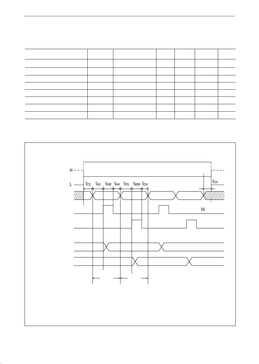
Switching Characteristics
(1) WRITE mode
¡ SemiconductorMSM58321
= 5V ±5%, Ta = 25°C)
(V
DD
Rating Symbol Condition Max. Unit
CS setup time
CS hold time
Address setup time
Address write pulse width
Address hold time
Data setup time
Write pulse width
Data hold time
CS1
CS2
D0 ~ D3
(ADDRESS/DATA)
ADDRESS WRITE
t
CS
t
CH
t
AS
t
AW
t
AH
t
DS
t
WW
t
DH
H
tCStAStAWtAHtDStWWt
L
Min.
–
–
–
–
–
0.5
0.1
–
–
–
DH
Typ.
0
0
0
–
–
–
–
–
0
2
0
–
–
–
–
–
–
–
–
–
–
–
µs
µs
µs
µs
µs
µs
µs
µs
t
CH
High Impedance
WRITE
IC internal
ADDRESS
IC internal DATA
ADDRESS
DATA
Write Cycle
Note: ADDRESS WRITE and WRITE inputs are activated by the level, not by the edge.
10
Page 5
¡ Semiconductor MSM58321
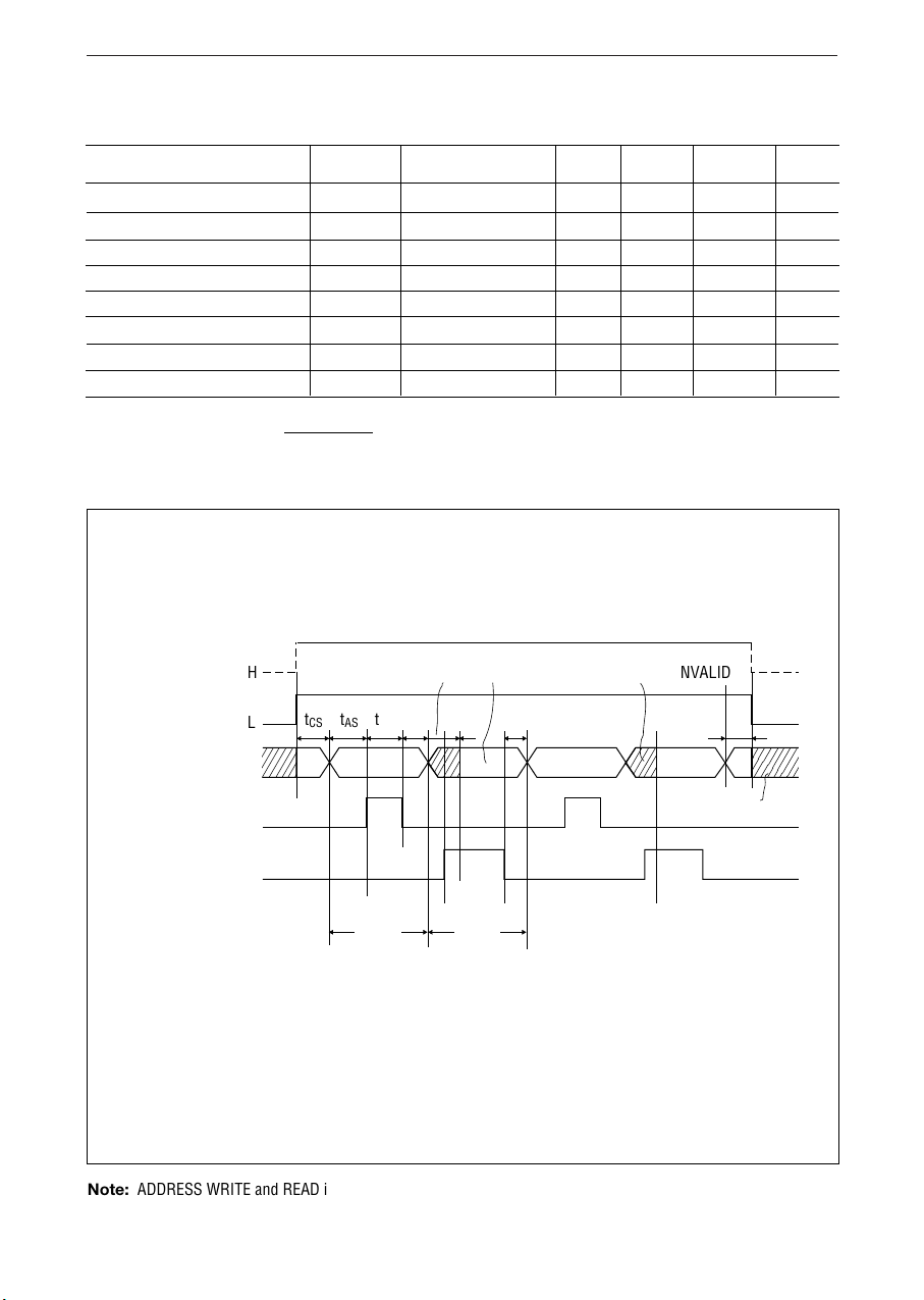
(2) READ mode
= 5V ±5%, Ta = 25°C)
(V
DD
Rating Symbol Condition Max. Unit
CS setup time
CS hold time
Address setup time
Address write pulse width
Address hold time
Read access time
Read delay time
Read inhibit time
Note 1. t
= 1 µs + CR ln ( )
RA
CS1
CS2
D0 ~ D3
(ADDRESS/DATA)
V
– VIH min
DD
H
tCStAStAWtRHt
L
0
0
0
–
–
0
Typ.
–
–
–
–
–
–
see Note 1
–
–
DATA INVALID
–
–
–
–
–
µs
µs
µs
µs
µs
µs
1
–
µs
µs
t
CH
Min.
t
RI
RA
–
–
–
–
–
–
–
–
DATA VALID
t
DD
0.5
0.1
t
CS
t
CH
t
AS
t
AW
t
AH
t
RA
t
DD
t
RI
V
DD
ADDRESS WRITE
READ
ADDRESS
DATA
Read Cycle
Note: ADDRESS WRITE and READ inputs are activated by the level, not by the edge.
High Impedance
11
Page 6

,
(3) WRITE & READ mode
¡ SemiconductorMSM58321
(VDD = 5V ±5%, Ta = 25°C)
Rating Symbol Condition Min.
CS setup time
CS hold time
Address setup time
Address write pulse width
Address hold time
Data setup time
Write pulse width
Data hold time
Read access time
Read delay time
Read inhibit time
= 1 µs + CR ln ( )Note 1.
t
RA
CS1
CS2
D0 ~ D3
(ADDRESS/DATA)
V
DD
– VIH min
V
DD
H
tCStAStAWtAHt
L
t
t
t
t
t
t
t
t
t
t
t
CS
CH
AS
AW
AH
DS
WW
DH
RA
DD
RI
Typ.
–
–
–
–
–
–
–
–
–
–
–
0.5
0.1
0
0
0
–
–
–
–
–
0
2
0
–
–
0
–
–
–
–
–
–
Max. Unit
–
–
–
–
–
–
–
–
see Note 1
1
–
µs
µs
µs
µs
µs
µs
µs
µs
µs
µs
µs
DATA INVALID
DATA VALID
t
RI
t
t
DS
WW
DH
t
RAtDD
t
CH
ADDRESS WRITE
High Impedance
WRITE
READ
IC internal
ADDRESS
IC internal DATA
ADDRESS
DATA WRITE
DATA READ
Read & Write Cycle
12
Page 7

¡ Semiconductor MSM58321
PIN DESCRIPTION
Name Pin No. Description
CS
2
CS
1
WRITE
1
Chip select pins. These pins enable the interface with the external circuit when
both of these pins are set at H level simultaneously.
13
If one of these pins is set at L level, STOP, TEST, WRITE, READ, ADDRESS
WRITE pins and D0 ~ D3 pins are inactivated.
Since the threshold voltage VT for the CS1 pin is higher than that for other pins,
it shuold be connected to the detector of power circuit and peripherals and CS
2
is to be connected to the microcontroller.
2
WRITE pin is used to write data; it is activated when it is at the H level. Data bus
data inside the IC is loaded to the object digit while this WRITE pin is at the H
level, not at the WRITE input edge. Refer to Figure 1 below.
(S1 digit)
D0 D3
Q
SR
Q
SR
WRITE
D0
D1
DATA BUS
D2
D3
S1
CS1 = CS2 = "H"
D0
H
S1
WRITE
F/F D0-θ
Figure 1
13
Page 8

Name Pin No. Description
¡ SemiconductorMSM58321
READ READ pin is used to read data; it is activated when it is at the H level. Address
3
contents are latched with ADDRESS LATCH inside the IC at the D0 ~ D3 and
ADDRESS WRITE pins to select the object digit, then an H-level signal is input
to the READ pin to read data.
If a count operation is continued by setting the STOP input to the L level, read
operation must be performed, in principle, while the BUSY output is at the H
level. While the BUSY output is at the L level, count operations are performed
by digit counters and read data is not guaranteed, therefore, read operations are
inhibited in this period. Figure 2 shows a time chart of the BUSY output, 1 Hz
signal inside the IC, and READ input.
A read operation is stopped temporarily within a period of 244 µs from the BUSY
output trailing edge and it is restarted when the BUSY output goes to the H level
again.
427 µs
BUSY
1 Hz (inside IC)
Read-enabled
period
244 µs
122 µs
Read-inhibited period
Read operation is enabled in this period:
however, it is used for program switching.
The counter inside the IC
starts counting at the
1 Hz signal leading edge.
Read-enabled period
61 µs
14
BUSY
1 Hz (inside IC)
READ input
1 sec
Figure 2
If the counter operation is stopped by setting the STOP input to the H level, read
operations are enabled regardless of the BUSY output.
A read operation is enabled by microcomputer software regardless of the BUSY
output during the counter operation by setting the STOP input to the L level.
In this method, read operations are performed two or more times continuously
and data that matches twice is used as guaranteed data.
Page 9

¡ Semiconductor MSM58321
Name Pin No. Description
D0 ~ D
GND
ADDRESS
WRITE
BUSY
3
4 ~ 7
Data input/output pins. (Bidirectional bus). The output is a open-drain type and
4.7 kΩ ~ 10 kΩ pull-up registers are required utilize these pins as output pins.
8
9
Ground pin.
ADDRESS WRITE pin is used to load address information from the D0 ~ D3 I/O
bus pins to the ADDRESS LATCH inside the IC; it is activated when it is at the H
level. This input is activated by the level, not by the edge. Figure 3 shows the
relationships between the D0 address input, ADDRESS WRITE input, and
ADDRESS LATCH input/output.
D0 input
ADDRESS WRITE
DI
0
ADDRESS LATCH
(inside IC)
L
DO
0
LATCH output
Figure 3
10
BUSY pin outputs the IC operation state. It is N-channel MOSFET open-drain
output. An external pull-up resistor of 4.6 kΩ or more must be connected (see
Figure 4) to use the BUSY output. The signals are output in negative logics. If
the oscillator oscillates at 32.768 kHz, the frequency is always 1 Hz regardless of
the CS1 and CS2 unless the D output of the ADDRESS DECODER inside the IC
is H (CODE = H•L•H•H) and CS1 = CS2 = WRITE = H.
Figure 5 shows the BUSY output time chart.
(peripheral circuit power)
4.7 kΩ or more
+5V
BUSY
RESET
N
MSM58321RS
BUSY
D
WRITE
Figure 4
BUSY
1 Hz (inside IC)
BUSY
1 Hz (inside IC)
244 µs
122 µs
427 µs
Read/write-inhibited period
1 sec
Figure 5
61 µs
The counter inside the IC
starts counting at the
1 Hz signal leading edge.
15
Page 10

Name Pin No. Description
¡ SemiconductorMSM58321
STOP The STOP pin is used to input on/off control for a 1 Hz signal. When this pin
11
goes to the H level, 1 Hz signals are inhibited and counting for all digits
succeeding the S1 digit is stopped. When this pin goes to the L level, normal
operations are performed; the digits are counted up. This STOP input controls
stopping digit counting. Writing of external data in digits can be assured by
setting the STOP input to the H level to stop counting, then writing sequentially
from the low-order digits.
TEST 12
The TEST pin is used to test this IC; it is normally open or connected to GND. It
is recommended to connect it to GND to safeguard against malfunctions from
noise.
The TEST pulse can be input to the following nine digits:
S1, S10, MI10, H1, D1 (W), M01, Y1 and Y10
When a TEST pulse is input to the D1 digit, the W digit is also counted up
simultaneously.
Input a TEST pulse as follows:
Set the address to either digit explained above, then input a pulse to the TEST pin
while CS1 = CS2 = STOP = H and WRITE = L. The specified and succeeding digits
are counted up. (See Figure 6)
TEST
1 Hz
R
p
C-S
0 ~ 9 0 ~ 9
C1
C10
S1
TEST-P
S1 S10 MI1
0 ~ 9 0 ~ 6
C0
D1
0 ~ 5
C10 C10
S10 MI1
C1
W
C1
D10
16
D1
Rp = 200 kΩ TYP
Figure 6
A digit is counted up at the leading edge (changing point from L to H) of a TEST
pin input pulse. The pulse condition for TEST pin input at VDD = 5V ±5% is
described in Figure 7 below.
t
H
t
L
tH = 10 µs MIN
tL = 10 µs MIN
Figure 7
Page 11

¡ Semiconductor MSM58321
Name Pin No. Description
XT Oscillator pin. A 32.768 kHz crystal oscillator, capacitor and trim capacitor for
XT 15
14
frequency adjustment are to be connected as shown in Figure 8 below.
RFB = 10 MΩ TYP
RS = 200 kΩ typ
GND or V
XT
C1
DD
C2
X-TAL 32.768 kHz, The crystal impedance is 30 kΩ or less.
R
FB
XT
RS
MSM58321
Figure 8
If an external clock is to be used for MSM58321's oscillation source, the
external clock is to be input to XT, while XT should be left open. Refer to the
Figure 9 below.
CMOS
XT
or +5V
XT
MSM58321
TTL
Figure 9
V
DD
16
Power supply pin. Refer to the application circuit.
17
Page 12

REFERENCE SIGNAL OUTPUT
Reference signals are output from the D
~ D3 pins under the following conditions:
0
¡ SemiconductorMSM58321
Conditions
WRITE = L
READ = H
CS1 = CS2 = H
ADDRESS = E or F
1024 Hz
1 Hz
1/60 Hz
1/3600 Hz
Output
pin
D
0
D
1
D
2
D
3
Reference signal
frequency
Pulse width
1024 Hz
1 Hz
1/60 Hz
1/3600 Hz
488.3 µs 488.3 µs
488.3 µs
122.1 µs
122.1 µs
122.1 µs
Output logic
Pisitive logic
Negative logic
Negative logic
Netgative logic
18
1 Hz
(inside IC)
BUSY
244 µs
Figure 10
122 µs 61 µs
-3
122.1 µs = x4
488.3 µs = x16
10
32,768
-3
10
32,768
Page 13

¡ Semiconductor MSM58321
APPLICATION NOTES
WRITE and STOP
Note that the timing relationship between the STOP and WRITE inputs vary by the related digit when counting is
stopped by the STOP input to write data. The time (tSH) between the STOP input leading edge and WRITE input
trailing edge for each digit is limited to the minimum value. (See Figure 11)
at VDD = 5V±5%
STOP
t
SHS1
t
SHH10
t
SHMO10
WRITE
= 1 µs, t
= 6 µs, t
= 10 µs, t
S1S10MI1MI10H
H
D1(W) D10MO1MO10Y1Y
10
1
123456789101112
t
SHS1
t
SHS10
t
SHY10
Write-inhibited period
Figure 11
SHS10
SHD1
= 2 µs, t
= 7 µs, t
= 11 µs, t
SHY1
SHMI1
SHW
= 3 µs, t
= 7 µs, t
= 12 µs.
SHY10
SHM10
SHD10
= 4 µs, t
= 8 µs, t
SHH1
SHM01
= 5 µs
= 9 µs
10
19
Page 14

¡ SemiconductorMSM58321
If a count operation is continued by setting the STOP input to the L level, write operation must be performed, in
principle, while the BUSY output is at the H level. While the BUSY output is at the L level, count operations are
performed by the digit counters and write operation is inhibited, but there is a marginal period of 244 µs from the
BUSY output trailing edge. If the BUSY output goes to the L level during a write operation, the write operation is
stopped temporarily within 244 µs and it is restarted when the BUSY output goes to the H level again. Figure 12
shows a time chart of BUSY output, 1 Hz signal inside the IC, and WRITE input.
BUSY
1 Hz (inside IC)
WRITE input
1 sec
Figure 12
Frequency divider and BUSY circuit reset
If A0 ~ A3 = H•L•H•H is input to ADDRESS DECODER, the DECODER output (D) goes to the H level. If CS1 = CS2 =
H and WRITE = H in this state, the 5 poststage in the 15-stage frequency divider and the BUSY circuit are reset.
In this period, the BUSY output remains at the H level and the 1 Hz signal inside the IC remains at the L level, and
counting is stopped. If this reset is inactivated while the oscillator operates, the BUSY output goes to the L level after
1000.1221 ±31.25 ms and the 1 Hz signal inside the IC goes to the H level after 1000.3663 ±31.25 ms. These times
are not the same because the first ten stages in the 15-stage frequency divider are not reset. (See Figure 13)
15-stage
frequency
O
15
(inside IC)
32,768 kHz
BUSY
STOP
WRITE
divider
circuit
1~10 stage
OSC
N RESET
R
p
R
p
CS
Stages
11~15
015
R
From ADDRESS DECODER
A0 A1 A2 A3
H L H H
BUSY
R
WRITE
D
t3
1 Hz
STOP
20
1 Hz
(inside IC)
RESET (inside IC)
t1 = 1000.1221 ±31.25 ms
t2 = 1000.3663 ±31.25 ms
t3 = 1000 ±31.25 ms
Figure 13
t1
t2
Page 15

¡ Semiconductor MSM58321
Selection of leap year
This IC is designed to select leap year automatically.
Four types of leap years can be selected by writing a select signal in the D2 and D3 bits of the D10 digit (CODE =
L•L•L•H). (See table 1 for the functions.)
Gregorian calendar or other calendars can be set arbitrarily in the Y1 and Y10 digits of this IC. There is a leap year
every four years and the year number varies according to the calendar used. There are four combinations of year
numbers and leap years. (See the Table below).
No. 1: Gregorian calendar year. The remainder obtained by dividing the leap year number by 4 is 0.
No. 2: The remainder obtained by dividing the leap year number by 4 is 3.
No. 3: The remainder obtained by dividing the leap year number by 4 is 2.
No. 4: The remainder obtained by dividing the leap year number by 4 is 1.
No.1 Calendar
Gregorian1
2
3
4
D10 digit
D2 D3
L
H
L
H
Remainder obtained by
dividing the leap year number by 4
L
L
H
H
Leap years (examples)
0
3
2
1
1980, 1984, 1988, 1992
1996, 2000, 2004
(83) (87) (91) (95) (99)
55, 59, 63, 67, 71,
75, 79
82, 86, 90, 94, 98,
102, 106
81, 85, 89, 93, 97,
101, 105
21
Page 16

APPLICATION EXAMPLE – POWER SUPPLY CIRCUIT
¡ SemiconductorMSM58321
RL
A495
10K
VF = 0.69V
100Ω
1.2x3 = 3.6V
Ni-Cd battery
C372
RL
M
B
+
–
+
VCE (Sat) = 0.1V
100Ω
100Ω
C
1.5x2 = 3V
Dry cell
Ripple
4.7µ
+
–
4.7µ
+
–
+
–
4.7µ
+
–
V
DD
GND
Operating state
Backup
MSM58321
Ripple
Operating state
V
DD
GND
V
DD
GND
Backup
MSM58321
MSM58321
20 mV P-P
0 mV
20 mV P-P
0 mV
+5.7V
a)
b)
c)
1S1588
or
C372
V
= 0.69
F
51K
10K
+5V
(Recommended circuit)
+V
(Power voltage
approximately
1.5V higher than
5V)
d)
+5V
(Peripheral
circuit power)
3.6V
Ni-Cd
battery
D1 D2
R2
+
–
100Ω
4.7µ
V
GND
DD
MSM58321
Note: Use the same diodes for D1 and D2 to reduce the level difference between +5V and VDD of the MSM58321.
22
 Loading...