

Datasheet MSM5718C50-60GS-K, MD5764802-53MC, MSM5718C50-53GS-K, MD5764802-60MC Datasheet (OKI)
Page 1

E2G1059-39-21
¡ Semiconductor MSM5718C50/MD5764802
¡ Semiconductor
This version: Feb. 1999
Previous version: Nov. 1998
MSM5718C50/MD5764802
18Mb (2M
¥¥
¥ 9) & 64Mb (8M
¥¥
DESCRIPTION
The 18/64-Megabit Concurrent Rambus™ DRAMs (RDRAM®) are extremely high-speed
CMOS DRAMs organized as 2M or 8M words by 8 or 9 bits. They are capable of bursting unlimited
lengths of data at 1.67 ns per byte (13.3 ns per eight bytes). The use of Rambus Signaling Level (RSL)
technology permits 600 MHz transfer rates while using conventional system and board design
methodologies. Low effective latency is attained by operating the two or four 2KB sense amplifiers
as high speed caches, and by using random access mode (page mode) to facilitate large block
transfers. Concurrent (simultaneous) bank operations permit high effective bandwidth using
interleaved transactions.
RDRAMs are general purpose high-performance memory devices suitable for use in a broad range
of applications including PC and consumer main memory, graphics, video, and any other
application where high-performance at low cost is required.
¥¥
¥ 8) Concurrent RDRAM
¥¥
FEATURES
• Compatible with Base RDRAMs
• 600 MB/s peak transfer rate per RDRAM
• Rambus Signaling Level (RSL) interface
• Synchronous, concurrent protocol for block-oriented, interleaved (overlapped) transfers
• 480 MB/s effective bandwidth for random 32 byte transfers from one RDRAM
• 13 active signals require just 32 total pins on the controller interface (including power)
• 3.3 V operation
• Additional/multiple Rambus Channels each provide an additional 600 MB/s bandwidth
• Two or four 2KByte sense amplifiers may be operated as caches for low latency access
• Random access mode enables any burst order at full bandwidth within a page
• Graphics features include write-per-bit and mask-per-bit operations
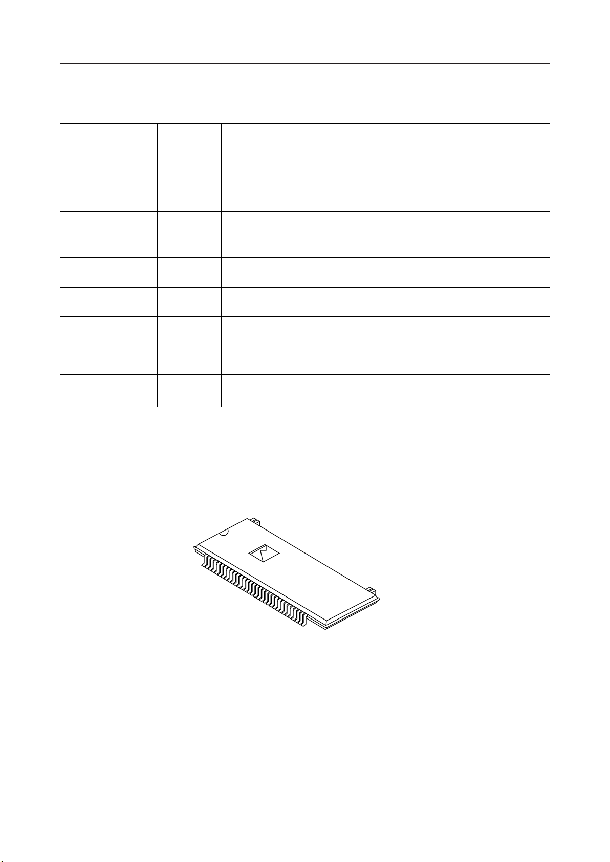
• Available in horizontal surface mount plastic package (SHP32-P-1125-0.65-K)
1/45
Page 2

¡ Semiconductor MSM5718C50/MD5764802
PART NUMBERS
The 18- and 64-Megabit RDRAMs are available in horizontal surface mount plastic package
(SHP),
with 533 and 600 MHz clock rate. The part numbers for the various options are shown in Table 1.
Table 1 Part Numbers by Option
533 MHzOptions 600 MHz
18-Megabit SHP
64-Megabit SHP
MSM5718C50-53GS-K
MD5764802-53MC
MSM5718C50-60GS-K
MD5764802-60MC
2/45
Page 3
¡ Semiconductor MSM5718C50/MD5764802
RDRAM PACKAGES AND PINOUTS
RDRAMs are available in horizontal surface mount plastic package (SHP).
The package has 32 signal pins and four mechanical pins that provide support for the device. The
mechanical pins are located on the opposite side from the signal leads in the SHP.
VDD 1
GND
DQ8
GND
DQ7
NC (18M) ; VREF (64M)
ADDRESS
VDD
DQ6
GND
DQ5
VDDA
RXCLK
GNDA
TXCLK
VDD
DQ4
GND
COMMAND
SIN
VREF
SOUT
DQ3
GND
DQ2
(NC)
DQ1
GND
DQ0
(NC)
GND
VDD
2
3
4
5
6
7
8
9
10
11
12
13
14
15
16
17
18
19
20
21
22
23
24
25
26
27
28
29
30
31
32
Fig. 1 SHP Pin Numbering
3/45
Page 4
¡ Semiconductor MSM5718C50/MD5764802
Table 2 Pin Descriptions
Signal I/O Description
DQ8..DQ0
(BUSDATA [8:0])
I/O
CLK
(RXCLK)
CLK
(TXCLK)
VREF I
COMMAND
(BUSCTRL)
ADDRESS
(BUSENABLE)
VDD, VDDA
GND, GNDA
—
—
SIN I
SOUT O
I
I
I
I
Signal lines for REQ, DIN, and DOUT packets. The REQ packet contains the
address field, command field, and other control fields. These are RSL
signals.
a
Receive clock. All input packets are aligned to this clock. This is an RSL
a
signal.
Transmit clock. DOUT packets are aligned with this clock. This is an RSL
a
signal.
Logic threshold reference voltage for RSL signals.
Signal line for REQ, RSTRB, RTERM, WSTRB, WTERM, RESET, and CKE
packets. This is an RSL signal.
Signal line for COL packets with column addresses. This is an RSL signal.
a
a
+3.3 V power supply. VDDA is a separate analog supply for clock generation
in the RDRAM.
Circuit ground. GNDA is a separate analog ground for clock generation in
the RDRAM.
Initialization daisy chain input. CMOS levels.
Initialization daisy chain output. CMOS levels.
a. RSL stands for Rambus Signaling Levels, a low-voltage-swing, active-low signaling technology.
Mechanical
Support Pins
Pin 1
Mechanical
Support Pins
Pin 32
Fig. 2 SHP Package
4/45
Page 5

¡ Semiconductor MSM5718C50/MD5764802
GENERAL DESCRIPTION
Figure 3 is a block diagram of an RDRAM. At the bottom is a standard DRAM core organized as two
or four independent banks, with each bank organized as 512 or 1024 rows, and with each row
consisting of 2KBytes of memory cells. One row of a bank may be “activated” at any time (ACTV
command) and placed in the 2KByte “page” for the bank. Column accesses (READ and WRITE
commands) may be made to this active page.
The smallest block of memory that may be accessed with READ and WRITE commands is an octbyte
(eight bytes). Bitmask and bytemask options are available with the WRITE command to allow finer
write granularity. There are six control registers that are accessed at initialization time to configure
the RDRAM for a particular application.
5/45
Page 6

¡ Semiconductor MSM5718C50/MD5764802
SIN
SOUT
RXCLK
ADDRESS
(BUSENABLE)
COMMAND
(BUSCTRL)
DQ8, DQ7,...DQ0
(BUSDATA[8:0])
TXCLK
11
Initialize/Powerdown
REQ
RSTRB, RTERM
WSTRB, WTERM
88
CKE, RESET
Control Logic
d64/72:
64/72
1
1
1
1
1
1
99
91
1:8 Demux 8:1 Mux
DIN 64/72
DEVICETYPE Register
DEVICEID Register
MODE Register
DOUT
REFROW Register
RASINTERVAL
DEVICEMFGR Register
64/72
64b for 64M
72b for 18M
d
64/72
d
64/72
64/72
Register
d
1
64/72
MASK Register
64/72
d
d
64/72 ¥ 256 Page
64/72 ¥ 256
64/72 ¥ 256 ¥ 1024
c
Bank 3
c
4 banks per RDRAM for 64M
64/72 ¥ 256 Page
64/72 ¥ 256
64/72 ¥ 256 ¥ 1024
Bank 2
c
64/72 ¥ 256a Page
64/72 ¥ 256
64/72 ¥ 256a ¥ 512
Bank 1
a
256 octbytes per row for 18M
b
512 rows per bank for 18M
64/72 ¥ 256a ¥ 512
Bank 1
a
256 octbytes per row for 64M
b
1024 rows per bank for 64M
64/72 ¥ 256a Page
a
b
64/72 ¥ 256a ¥ 512
64/72 ¥ 256
a
b
Bank 0
b
64/72 ¥ 256
a
¥ 512
b
Bank 0
Fig. 3 18/64-Mbit Concurrent RDRAM Block Diagram
6/45
Page 7
¡ Semiconductor MSM5718C50/MD5764802
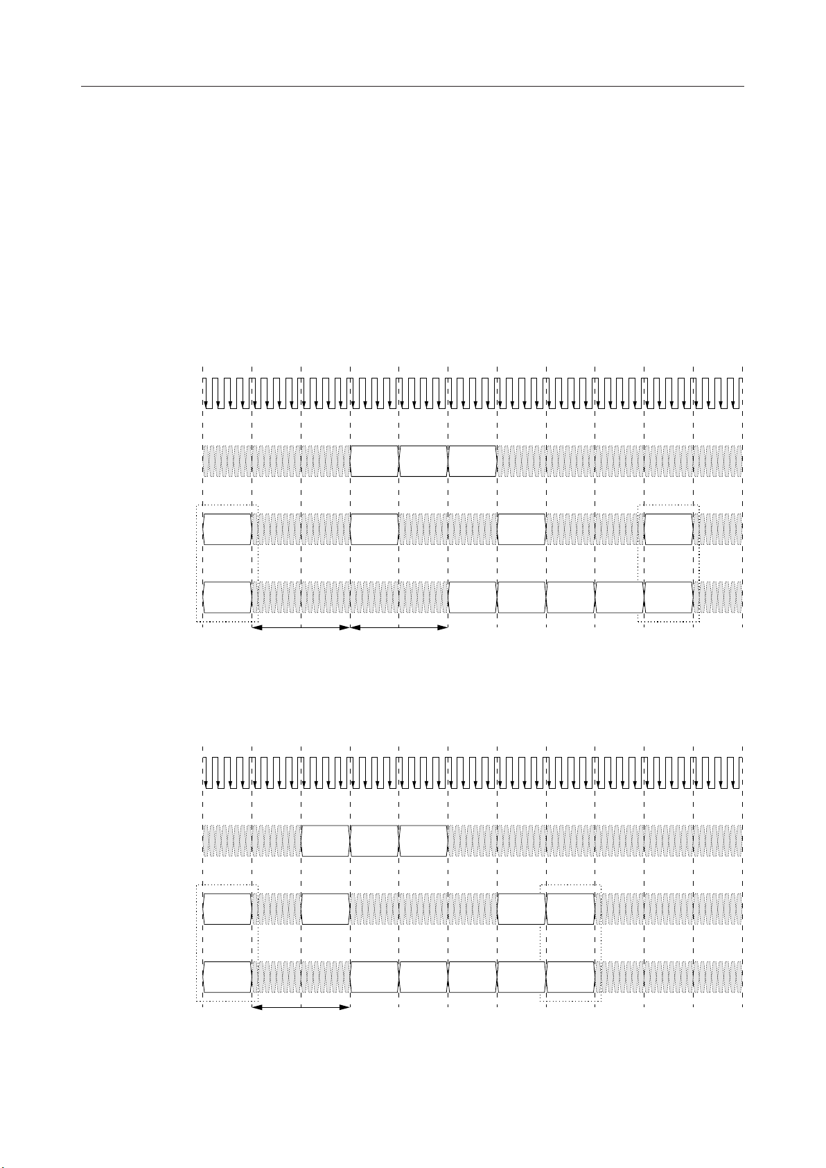
BASIC OPERATION
Figure 4 (a) shows an example of a read transaction. A transaction begins in interval T0 with the
transfer of a REQ packet. The REQ packet contains the command (ACTV/READ), a device, bank,
and row address (BNK/ROW) of the page to be activated, and the column address (COLa) of the first
octbyte to be read from the page.
The selected bank performs the activation of the selected row during T1 and T2 (the t
Next, the selected bank reads the selected octbyte during T3 and T4 (the t
interval). A second
CAC
RCD
interval).
command RSTRB (read strobe) is transferred during T3 and causes the first octbyte (DOUTa) to be
transferred during T5.
T
9
10
CLK
(RX/TXCLK)
ADDRESS
(BUSENABLE)
COMMAND
(BUSCTRL)
DQ8,..DQ0
(BUSDATA[8:0])
Bank Operation
T
0
ACTV
/READ
REQ
Packet
BNK/ROW
/COL a
T
1
T
2
T
3
T
4
T
5
T
6
T
7
T
T
8
COL b COL c COL d
RSTRB RTERM
Next
REQ
DOUT a DOUT b DOUT c DOUT d
t
RCD
t
CAC
CLK
(RX/TXCLK)
ADDRESS
(BUSENABLE)
COMMAND
(BUSCTRL)
DQ8,..DQ0
(BUSDATA[8:0])
Bank Operation
(b) BANK ACTIVATE AND RANDOM WRITE CYCLES WITHIN A PAGE
(a) BANK ACTIVATE AND RANDOM READ CYCLES WITHIN A PAGE
T
0
T
1
T
2
T
3
T
4
T
5
T
6
T
7
T
8
COL b COL c COL d
ACTV
/WRITE
REQ
Packet
BNK/ROW
/COL a
WSTRB WTERM
DIN a DIN b DIN c DIN d
t
RCD
Next
REQ
T
T
9
10
Fig. 4 Read and Write Transaction Examples
7/45
Page 8

¡ Semiconductor MSM5718C50/MD5764802
In this example, three additional octbytes are read from the activated page. These column addresses
(COLb, COLc, and COLd) are transferred in T3, T4, and T5, respectively. The data octbytes (DOUTb,
DOUTc, and DOUTd) are transferred in T6, T7, and T8, The end of the data octbytes is signaled by
a third command RTERM (read terminate) in T6. The next REQ packet may be sent in T9, or in any
interval thereafter.
Figure 4 (b) shows an example of a write transaction. The transaction begins in interval T0 with the
transfer of a REQ packet. The REQ packet contains, the command (ACTV/WRITE), a device, bank,
and row address (BNK/ROW) of the page to be activated, and the column address (COLa) of the first
octbyte to be written to the page.
The selected bank performs the activation of the selected row during T1 and T2 (the t
RCD
interval).
A second command WSTRB (write strobe) is transferred during T2 and causes the first octbyte
(DINa) to be transferred during T3.
In this example, three additional octbytes are written to the activated page. These column addresses
(COLb, COLc, and COLd) are transferred in T2, T3, and T4 respectively. The data octbytes (DINb,
DINc, and DINd) are transferred in T4, T5, and T6. The end of the data octbytes is signaled by a third
command WTERM (write termination) in T6. The next REQ packet may be sent in T7, or in any
interval thereafter.
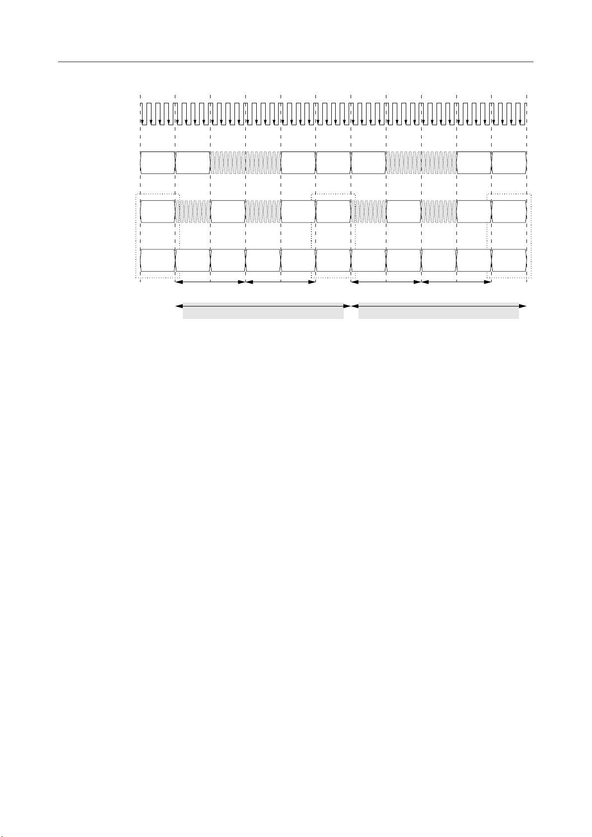
INTERLEAVED TRANSACTIONS
The previous examples showed noninterleaved transactions - the next REQ packet was transferred
after the last data octbyte of the current transaction. In an interleaved transaction, the next REQ packet
is transferred before the first data octbyte of the current transaction. This permits the row and column
access intervals of the next transaction to overlap the data transfer of the current transaction.
Figure 5 shows an example of interleaved read transactions. The first transaction proceeds exactly
as the noninterleaved example of Figure 4 (a) (all packets of the first transaction are labeled with “1”).
However, in T5 the REQ packet for the second transaction is transferred (all packets of the second
transaction are labeled with “2”). The t
octbytes and thus increase the effective bandwidth of the RDRAM since there are no unused
intervals.
RCD2
and t
intervals overlap the transfer of DOUT1 data
CAC2
A transaction consists of an address transfer phase and a data transfer phase. The REQ packet
performs address transfer, and the remaining packets perform data transfer (DOUT, COL, RSTRB,
and RTERM in the case of a read transaction). The time interval between the address and data transfer
phases of the current transaction may be adjusted to match the data length of the previous transaction
(as long as the row and column access times for the current transaction are observed). Thus, there ar e
no limits on the types of memory transaction which may be interleaved; any mixing of transaction
length and command type is permitted.
8/45
Page 9
¡ Semiconductor MSM5718C50/MD5764802
CLK
(RX/TXCLK)
ADDRESS
(BUSENABLE)
COMMAND
(BUSCTRL)
DQ8,..DQ0
(BUSDATA[8:0])
Bank Operation
T
T
0
T
1
2
T
T
3
4
COL c0 COL d0 COL b1
ACTV
/READ
RTERM1
RSTRB1
REQ
Packet 1
BNK/ROW
/COL a1
DOUT a0 DOUT b0 DOUT c0 DOUT d0
t
RCD1
Data Transport 0 Overlaps Row/Column Access 1 Data Transport 1 Overlaps Row/Column Access 2
t
CAC1
Fig. 5 Interleaved Read Transaction Example
T
5
T
T
6
T
7
T
8
T
9
10
COL c1 COL d1 COL b2 COL c2
ACTV
/READ
REQ
Packet 2
BNK/ROW
/COL a2
RTERM2
RSTRB2
DOUT a1 DOUT b1 DOUT c1 DOUT d1
t
RCD2
t
CAC2
ACTV
/READ
REQ
Packet 3
BNK/ROW
/COL a3
9/45
Page 10
¡ Semiconductor MSM5718C50/MD5764802
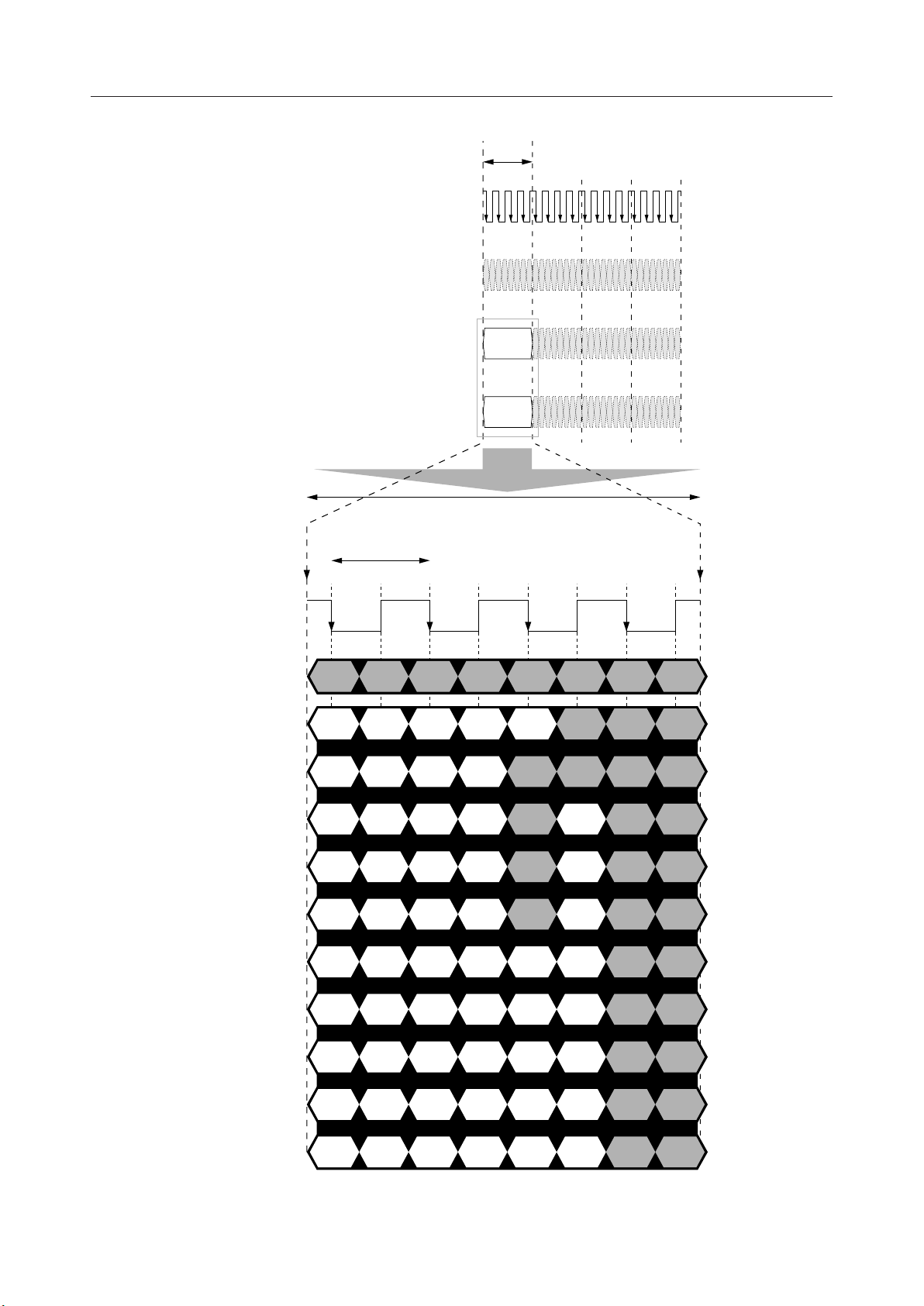
REQ PACKET (ADDRESS TRANSFER)
An REQ packet initiates a transaction by transferring the address and command information to the
RDRAM. Figure 6 shows the format of the REQ packet. Note that each RDRAM wire carries eight
bits of information in each t
PACKET
natural granularity with which to illustrate timing relationships. The clock that is actually used by
the RDRAM has a period of t
times t
CYCLE
.
CYCLE
In the REQ packet, the bits which are gray are reserved, and should be driven with a zero. In
particular, the bits in t
CYCLE t6
A35..A3: The address field A35..A3 consumes the greatest number of bits. These are allocated to
device, bank, row, and column addressing according to Table 3:
. This is the time required to transfer an octbyte of data and is the
, with information transferred on each clock edge. t
PACKET
is four
and t7 are needed for bus-turn-around during read transactions.
Table 3 A35..A3 Address Fields
Field 18M
COL A10..A3
ROW A19..A11
BNK A20
DEV A35..A21
64M
A10..A3
A20..A11
A22, A21
A35..A23
OP5..OP0: The command field OP5..OP0 specifies the type of transaction that is to be performed,
according to Table 4. The OP0 bit selects a read or write transaction, the OP1 bit selects a memory or
register space access, and OP5..OP2 select command options. These command options include B in
OP2 (see byte masking on page 22). D in OP3 for selecting broadcast operations (see refresh on page
35), and b1, b0 in OP5, OP4 (see bit masking on page 23).
ACTV: This bit specifies activation or precharge/activation of a bank at the beginning of a
transaction, and is designated by prepending “ACTV/” or “PRE/ACTV/” to the command.
AUTO: This bit specifies auto-precharge of a bank at the end of the transaction, and is designated
by appending “A” to the command.
START: This bit is always set to a one and indicates the beginning of a request to the RDRAM.
REGSEL: This bit is used for accessing registers.
PEND2...PEND0: This field is set to “000” for noninterleaved transactions, and to a nonzero value
for interleaved transactions. This is the number of previous STRB and TERM packets the RDRAM
is to skip. Refer to the
Concurrent RDRAM Design Guide
for further details.
M7..M0: This field is used to perform byte masking of the first data octbyte DINa for all memory write
transactions (OP1, OP0 = 01). Refer to byte masking on page 22.
10/45
Page 11
¡ Semiconductor MSM5718C50/MD5764802
Table 4 Command Encoding
ACTV AUTO
00000X00READ Read
0 0 b1 b0 D B 0 1 WRITE Write
00000110RREG Register Read
0000D111WREG Register Write (D)
01000X00READA Read/AutoPrecharge
0 1 b1 b0 D B 0 1 WRITEA Write/AutoPrecharge (b1, b0, D, B)
10000X00ACTV/READ Activate/Read
1 0 b1 b0 D B 0 1 ACTV/WRITE Activate/Write (b1, b0, D, B)
11000X00ACTV/READA Activate/Read/AutoPrecharge
1 1 b1 b0 D B 0 1 ACTV/WRITEA Activate/Write/AutoPrecharge (b1, b0, D, B)
10000X00PRE/ACTV/READ Precharge/Activate/Read
1 0 b1 b0 D B 0 1 PRE/ACTV/WRITE Precharge/Activate/Write (b1, b0, D, B)
11000X00PRE/ACTV/READA Precharge/Activate/Read/AutoPrecharge
1 1 b1 b0 D B 0 1 PRE/ACTV/WRITEA
OP5 OP4 OP3 OP2 OP1 OP0 Command Description
(b1, b0, B masking and D broadcast options)
Precharge/Activate/Write/AutoPrecharge (b1, b0, D, B)
11/45
Page 12
¡ Semiconductor MSM5718C50/MD5764802
t
PACKET
CLK
T
T
0
T
1
T
2
3
CLK
(RX/TXCLK)
ADDRESS
(BUSENABLE)
COMMAND
(BUSCTRL)
ACTV
/READ
REQ
Packet
DQ8,..DQ0
(BUSDATA[8:0])
t
CYCLE
t
t
0
t
1
2
t
PACKET
t
BNK/ROW
/COL a
= 4 • t
T
0
3
t
4
CYCLE
t
t
5
t
6
7
ADDRESS
COMMAND
DQ8
DQ7
DQ6
DQ5
DQ4
DQ3
DQ2
DQ1
OP4OP2OP5OP1START
A35A26OP3OP0
A34A25A17A9
A33A24A16A8
A32A23A15A7
A31A22A14A6
ACTV
A30A21A13A5
AUTO
A29A20A12A4
PEND2
A28A19A11A3
PEND1
M7
M6
M5
M4
M3
M2
M1
DQ0
REGSEL
A27A18A10
Fig. 6 REQ Packet Format
PEND0
M0
12/45
Page 13

¡ Semiconductor MSM5718C50/MD5764802
DATA TRANSFER PACKETS
The next set of packet types are used for data transfer. Their formats are summarized in Figure 7.
As in the REQ packet, eight bits are transferred on each wire during each t
PACKET
interval. The rising
and falling edges of the RDRAM clock define the transfer windows for each of these bits. The data
transfer packets will align to the t
PACKET
intervals defined by the START bit of the REQ packet by
simply observing the timing rules that are developed in the next few sections of this document.
DIN and DOUT Packets
There are nine wires allocated for the data bytes. These wires are labeled DQ8..DQ0. The eight bytes
transferred in a DIN or DOUT packet have 72 bits, which are labeled D0..D63 (on the DQ0..DQ7
wires) and E0..E7 (on the DQ8 wire). The 18Mbit RDRAM have storage cells for the E0..E7 bits. The
E0..E7 bits are also used with byte masking operations. This is described in the section on byte
masking on page 22.
COL Packet
The column address A10..A3 of the first octbyte of data (DINa or DOUTa) is provided in the REQ
packet. The COL packet contains an eight bit field A10..A3, which provides the column address for
the second and subsequent data octbytes. The COL packets have a fixed timing relationship with
respect to the DIN and DOUT packets to which they correspond. As the DIN and DOUT packets are
moved (to accommodate interleaving ), the COL packets move with them.
RSTRB and RTERM Packets
The RSTRB and RTERM packets indicate the beginning and end of the DOUT packets that are
transferred during a read transaction. The RSTRB and RTERM packets are each eight bits and consist
of a single “1” in an odd t
position, with the other seven positions “0”. Note that when a
CYCLE
transaction transfers a single data octbyte, the RSTRB and RTERM packets will overlay one another.
This is permitted and is in fact the reason that each packet consists of a single asserted bit. An example
of this case is shown in Figure 14 (a). There will be transaction situations in which the RTERM
overlays a RSTRB packet (two octbyte interleaved transaction). Again, this is permitted. The general
rule is that the RTERM may overlay any of the other packets on the Command (BUSCTRL) wire, and
RSTRB may overlay any other except for a REQ packet.
WSTRB and WTERM Packets
The WSTRB and WTERM packets indicate the beginning and end of the series of DIN packets that
are transferred during a write transaction. The WSTRB and WTERM packets are each eight bits and
consist of a single “1” in an odd t
position, with the other seven positions “0”. Note that when
CYCLE
a transaction transfers a single data octbyte, the WSTRB and WTERM packets will not overlay one
another (unlike the case of a one octbyte read). An example of this case is shown in Figure 14 (b). There
will be transaction situations in which the WSTRB overlays a REQ packet (no bank activate). Again,
this is permitted. An example of this is shown in Figure 9 (a). The general rule is that the WSTRB may
overlay any of the other packets on the Command (BUSCTRL) wire, and WTERM may overlay any
other except for a REQ packet.
13/45
Page 14

¡ Semiconductor MSM5718C50/MD5764802
CKE PACKET
The average power of the RDRAM can be reduced by using Suspend power mode. This is done by
setting the FR field of the MODE register to a zero (the MODE register is shown in Figure 17). A CKE
packet must be sent a time t
ahead of each REQ packet (this is shown in interval T0 in Figure 21
CKE
(b)). This causes the RDRAM to transition from Suspend to Enable mode. When the RDRAM has
finished the transaction, it returns to Suspend mode. The CKE packet will overlay the RSTRB and
RTERM packets when transactions are interleaved. If the FR field is set to a one, CKE packets are not
used and the RDRAM remains in Enable mode.
RESET PACKET
The RESET packet is used during initialization. When RESET packets are driven for a time t
RESET
or
greater, the RDRAM will assume a known state. Because the RESET packet is limited to this one use,
it will not interact with the other packet types. This is illustrated in Figure 21 (a).
PWRUP PACKET
The PWRUP packet is used to cause an RDRAM to transition from Powerdown to Enable mode. This
is illustrated in Figure 21 (c).
14/45
Page 15

¡ Semiconductor MSM5718C50/MD5764802
CLK
DQ8
DQ7
DQ6
DQ5
DQ4
DQ3
DQ2
DQ1
t
t
0
t
1
t
2
E3E2E1E0
D31D23D15D7
D30D22D14D6
D29D21D13D5
D28D20D12D4
D27D19D11D3
D26D18D10D2
D25D17D9D1
t
3
t
4
t
5
t
6
7
E7E6E5E4
D63D55D47D39
D62D54D46D38
D61D53D45D37
DIN a
DIN b
DIN c
DIN d
D60D52D44D36
D59D51D43D35
D58D50D42D34
D57D49D41D33
DOUT a
DOUT b
DOUT c
DQ0
CLK
ADDRESS
COMMAND
COMMAND
COMMAND
COMMAND
COMMAND
D24D16D8D0
t
t
0
t
1
t
2
t
3
t
4
t
5
D56D48D40D32
t
6
7
DOUT d
COL b
A6A5A4A3 A10A9A8A7
COL c
COL d
1
1
1
1
1
CKE
RSTRB
RTERM
WSTRB
WTERM
COMMAND
COMMAND
11111111
11111111
RESET
PWRUP
Fig. 7 DIN, DOUT, COL, CKE, RSTRB, RTERM, WSTRB, WTERM, and RESET Packet Formats
15/45
Page 16

¡ Semiconductor MSM5718C50/MD5764802
READ TRANSACTIONS
When a controller issues a read request to an RDRAM, one of three transaction cases will occur. This
is a function of the request address and the state of the RDRAM .
READ: The first case is shown in Figure 8 (a). This occurs when the requested bank has been left in
an activated state and the requested row address matches the address of this activated row. This is
also called a page hit read and is invoked by the READ or READA commands.
There are three timing parameters which specify the positioning of the packets which control the data
transfer. These are as follows:
t
SDR
t
CDR
t
TDR
These parameters are all expressed in units of t
Start of RSTRB to start of DOUT
Start of COL to start of DOUT
Start of RTERM to end of DOUT
CYCLE
, and the minimum and maximum values are
the same; the RSTRB, RTERM, COL, and DOUT packets move together as a block.
A fourth parameter has a minimum value only, and positions the block of data transfer packets
relative to the REQ (address transfer) packet:
t
RSR
Start of REQ to start of RSTRB for READ
When a read transaction is formed, these packet constraints must be observed. In addition, there are
constraints upon the timing of the bank operations which must also be observed. These are shown
in Figure 8 (a) next to the label “Bank Operation”. After the transfer of the REQ packet in T0, the
RDRAM performs a column access (requiring t
for the column access time) of the first data
CAC
octbyte DOUTa during T1 and T2. The RDRAM performs three column cycles (requiring tCC for the
column cycle time) in order to access the next three data octbytes (DOUTb. DOUTc, DOUTd) during
T3, T4 and T5. Each data octbyte is transferred one t
PACKET
interval after it is accessed.
ACTV/READ: The second case is shown in Figure 8 (b). This occurs when the requested bank has
been left in a precharged state. This is invoked by the ACTV/READ and ACTV/READA commands.
The RSTRB, RTERM, COL, and DOUT packets remain in the same relative positions as in the READ
case, but they move further from the REQ packet:
t
ASR
Start of REQ to start of RSTRB for ACTV/READ
After the transfer of the REQ packet in T0, the RDRAM performs an activation operation (requiring
t
for the row-column delay) during T1 and T2. This leaves the requested row activated. From this
RCD
point the sequence of bank operations are identical to the READ case, except that everything has
shifted two t
as t
(the row access time).
RAC
PACKET
intervals further from the REQ packet. The sum of t
RCD
and t
is also known
CAC
16/45
Page 17

¡ Semiconductor MSM5718C50/MD5764802
PRE/ACTV/READ: The third case is shown in Figure 8 (c). This occurs when the requested bank has
been left in an activated state and the requested row address doesn’t match the address of this
activated row. This is also called a page miss read and is invoked by the PRE/ACTV/READ and
PRE/ACTV/READA commands. The RDRAM knows the difference between a PRE/ACTV/
READ and a ACTV/READ because each RDRAM bank has a flag indicating whether it is precharged
or activated. The external controller tracks this flag, and also tracks the address of each activated bank
in order to distinguish READ and PRE/ACTV/READ accesses.
The RSTRB, RTERM, COL, and DOUT packets remain in the same relative positions as in the READ
case, but they move further from the REQ packet:
t
PSR
Start of REQ to start of RSTRB for PRE/ACTV/READ
After the transfer of the REQ packet in T0, the RDRAM performs a precharge operation (tRP) during
T1 and T2, and an activation operation (t
) during T3 and T4. This leaves the requested row
RCD
activated. From this point the sequence of bank operations are identical to the READ case, except that
everything has shifted four t
t
is also known as tRC (the row cycle time).
CAC
PACKET
intervals further from the REQ packet. The sum of tRP, t
RCD
, and
Auto-Precharge Option: For a READ, ACTV/READ, or a PRE/ACTV/READ command, the bank
operations are complete once the last data octbyte has been accessed. The bank will be left with the
requested row activated. For a READA, ACTV/READA, or a PRE/ACTV/READA command,
there is an additional step. During the two t
auto-precharge operation (requiring t
for the row precharge, auto) is performed. This leaves the
RPA
PACKET
intervals after the last data octbyte access, an
bank in a precharged state.
T
9
10
CLK
(RX/TXCLK)
T
T
0
T
1
2
T
3
T
T
4
T
5
6
T
7
T
8
T
ADDRESS
(BUSENABLE)
COMMAND
(BUSCTRL)
DQ8,..DQ0
(BUSDATA[8:0])
Bank Operation
COL b COL c COL d
t
t
SDR
CAC
t
CDR
RTERM
DOUT a DOUT b DOUT c DOUT d
t
CC
t
CC
t
TDR
t
CC
t
RPA
t
RSR
READA
REQ
Packet
BNK
/COL a
RSTRB
(a) READA - RANDOM READ CYCLES WITHIN A PAGE
17/45
Page 18

¡ Semiconductor MSM5718C50/MD5764802
T
T
0
T
1
2
T
T
3
T
4
5
T
T
6
T
7
CLK
(RX/TXCLK)
ADDRESS
(BUSENABLE)
COMMAND
(BUSCTRL)
DQ8,..DQ0
(BUSDATA[8:0])
Bank Operation
ACTV
/READA
REQ
Packet
BNK/ROW
/COL a
t
ASR
t
RCD
COL b COL c COL d
t
CDR
RSTRB RTERM
t
SDR
DOUT a DOUT b DOUT c DOUT d
t
RAC
t
CAC
t
CC
t
TDR
t
CC
t
CC
(b) ACTV/READA - BANK ACTIVATE AND RANDOM READ CYCLES WITHIN A PAGE
T
8
t
RPA
T
9
10
T
T
0
1
T
T
2
T
3
T
4
5
T
T
6
T
7
T
8
T
9
10
CLK
(RX/TXCLK)
ADDRESS
(BUSENABLE)
COMMAND
(BUSCTRL)
DQ8,..DQ0
(BUSDATA[8:0])
Bank Operation
PRE/ACTV
/READA
REQ
Packet
BNK/ROW
/COL a
t
PSR
t
RP
t
RCD
t
RC
COL b COL c COL d
t
CDR
RSTRB RTERM
t
SDR
DOUT a DOUT b DOUT c DOUT d
t
CAC
t
CC
t
CC
t
TDR
t
CC
t
RPA
(c) PRE/ACTV/READA - BANK PRECHARGE/ACTIVATE AND RANDOM READ CYCLES IN A PAGE
Fig. 8 Read Transactions
18/45
Page 19

¡ Semiconductor MSM5718C50/MD5764802
WRITE TRANSACTIONS
When a controller issues a write request to an RDRAM, one of three transaction cases will occur. This
is a function of the request address and the state of the RDRAM.
WRITE: The first case is shown in Figure 9 (a). This occurs when the requested bank has been left
in an activated state and the requested row address matches the address of this activated row. This
is called a page hit write and is invoked by the WRITE or WRITEA commands.
There are three timing parameters which specify the positioning of the packets which control the data
transfer. These are as follows:
t
SDW
t
CDW
t
TDW
These parameters are all expressed in units of t
Start of WSTRB to start of DIN
Start of COL to start of DIN
Start of WTERM to end of DIN
CYCLE
, and the minimum and maximum values are
the same; the WSTRB, WTERM, COL, and DIN packets move together as a block.
A fourth parameter has a minimum value only, and positions the block of data transfer packets
relative to the REQ (address transfer) packet:
t
WSW
Start of REQ to start of WSTRB for WRITE
When a write transaction is formed, these packet constraints must be observed. In addition, there are
constraints upon the timing of the bank operations which must also be observed. These are shown
in Figure 9 (a) next to the label “Bank Operation”. After the transfer of the REQ packet in T0, the
RDRAM performs a column access (requiring t
for the column access time) of the first data
CAC
octbyte DINa during T1 and T2, The RDRAM performs three column cycles (requiring tCC for the
column cycle time) in order to access the next three data octbytes (DINb, DINc. DINd) during T3, T
and T5. Each data octbyte is transferred one t
PACKET
interval before it is accessed.
ACTV/WRITE: The second case is shown in Figure 9 (b). This occurs when the requested bank has
been left in a precharged state. This is invoked by the ACTV/WRITE and ACTV/WRITEA
commands.
4
The WSTRB, WTERM, COL, and DIN packets remain in the same relative positions as in the page
hit case, but they move further from the REQ packet:
t
ASW
After the transfer of the REQ packet in T0, the RDRAM performs an activation operation (called t
Start of REQ to start of WSTRB for ACTV/WRITE
RCD
or row-column delay) during T1 and T2. This leaves the requested row activated. From this point the
sequence of bank operations are identical to the WRITE case, except that everything has shifted two
t
PACKET
intervals further from the REQ packet. The sum of t
RCD
and t
is also known as t
CAC
RAC
(the
row access time).
19/45
Page 20

¡ Semiconductor MSM5718C50/MD5764802
PRE/ACTV/WRITE: The third case is shown in Figure 9 (c). This occurs when the requested bank
has been left in an activated state and the requested row address doesn’t match the address of this
activated row. This is also called a page miss write and is invoked by the PRE/ACTV/WRITE and
PRE/ACTV/WRITEA commands. The RDRAM knows the difference between a PRE/ACTV/
WRITE and a ACTV/WRITE because each RDRAM bank has a flag indicating whether it is
precharged or activated. The external controller tracks this flag, and also tracks the address of each
activated bank in order to distinguish PRE/ACTV/WRITE and WRITE accesses.
The WSTRB, WTERM, COL, and DIN packets remain in the same relative positions as in the WRITE
case, but they move further from the REQ packet:
t
PSW
Start of REQ to start of WSTRB for PRE/ACTV/WRITE
After the transfer of the REQ packet in T0, the RDRAM performs a precharge operation (tRP) during
T1 and T2, and an activation operation (t
) of during T3 and T4. This leaves the requested row
RCD
activated. From this point the sequence of bank operations are identical to the WRITE case, except
that everything has shifted four t
and t
is also known as tRC (the row cycle time).
CAC
PACKET
intervals further from the REQ packet. The sum of tRP, t
RCD
Auto-Precharge Option: For a WRITE, ACTV/WRITE or a PRE/ACTV/WRITE command, the
bank operations are complete once the last data octbyte has been accessed. The bank will be left with
the requested row activated. For a WRITEA, ACTV/WRITEA or a PRE/ACTV/WRITEA command,
there is an additional step. During the two t
precharge operation (requiring t
for the row precharge, auto) is performed. This leaves the bank
RPA
PACKET
intervals after the last data octbyte access an auto-
in a precharged state.
T
9
10
CLK
(RX/TXCLK)
T
0
T
1
T
T
2
3
T
4
T
5
T
T
6
7
T
T
8
,
ADDRESS
(BUSENABLE)
t
WSW
COMMAND
(BUSCTRL)
DQ8,..DQ0
(BUSDATA[8:0])
Bank Operation
COL b COL c COL d
t
CDW
WSTRB
WRITEA
REQ
Packet
BNK/ROW
/COL a
t
SDW
DIN a DIN b DIN c DIN d
t
CAC
t
CC
WTERM
t
TDW
t
CC
t
CC
t
RPA
(a) WRITEA - RANDOM WRITE CYCLES WITHIN A PAGE
20/45
Page 21

¡ Semiconductor MSM5718C50/MD5764802
T
0
T
T
1
2
T
3
T
T
4
5
T
6
T
7
T
8
CLK
(RX/TXCLK)
ADDRESS
(BUSENABLE)
COMMAND
(BUSCTRL)
DQ8,..DQ0
(BUSDATA[8:0])
Bank Operation
t
ASW
ACTV
/WRITEA
REQ
Packet
BNK/ROW
/COL a
COL b COL c COL d
t
CDW
WSTRB
t
SDW
DIN a DIN b DIN c DIN d
t
RCD
t
RAC
t
CAC
t
CC
WTERM
t
TDW
t
CC
t
CC
t
RPA
(b) ACTV/WRITEA - BANK ACTIVATE AND RANDOM WRITE CYCLES WITHIN A PAGE
T
0
T
1
T
T
2
3
T
4
T
5
T
6
T
7
T
8
CLK
(RX/TXCLK)
T
T
T
9
9
10
T
10
ADDRESS
(BUSENABLE)
COMMAND
(BUSCTRL)
DQ8,..DQ0
(BUSDATA[8:0])
Bank Operation
ACTV
/WRITEA
REQ
Packet
BNK/ROW
/COL a
t
PSW
t
RP
COL b COL c COL d
t
CDW
WSTRB
t
SDW
t
RCD
t
RC
WTERM
t
TDW
DIN a DIN b DIN c DIN d
t
CAC
t
CC
t
CC
t
CC
t
RPA
(c) PRE/ACTV/WRITEA - BANK PRECHARGE/ACTIVATE AND RANDOM WRITE CYCLES IN A PAGE
Fig. 9 Write Transactions
21/45
Page 22

¡ Semiconductor MSM5718C50/MD5764802
BYTEMASK OPERATIONS
All memory write transactions (OP1,OP0 = 01) use the M7..M0 field of the REQ packet to control byte
masking of the first octbyte DINa of write data. M7 controls bits D56..D63,E7 while M0 controls bits
D0..D7, E0. A “0” means don’t write and a "1" means write.
The M7..M0 field should be filled with “00000000” for non-memory-write transactions.
OP2 = 1: When OP2 = 1 for a memory write transaction, the remaining data octbytes (DINb, DINc,...)
are written unconditionally (all bytes are written).
OP2 = 0: When OP2 = 0, the remaining data octbytes (DINb, DINc,...) are written with a bytemask.
Each bytemask is carried on the DQ8 wire, pipelined one t
PACKET
it controls.
Figure 12 (b) shows the format of the M packet and DIN packet when OP2 = 0. M7 controls bits
D56..D63 (of the next DIN packet) and M0 controls bits D0..D7 (of the next DIN packet). Figure 12
(a) summarizes the location of the M packets and the DIN packets they control.
interval ahead of the data octbyte
When 64M RDRAM is used, there is no limitation caused by the use of bytemask operations; the
DQ8 wire is only used for the REQ packet and M packets.
When 18M RDRAM is used, there is a limitation caused by the use of bytemask operations; the E7..E0
bits of the 72 bit DIN packet may not be used when OP2 = 0. To achieve bytemasking, it will be
necessary to use read-modify-write operations or single-octbyte writes with the bytemask in the
REQ packet and OP2 = 1.
DIN/DOUT
M7, M6,...M0 from REQ (Ma) and DQ8 (Mb, Mc,...)
64/72
64/72
64/72
Memory
Data
8
Fig. 10 Details of ByteMask Logic
22/45
Page 23

¡ Semiconductor MSM5718C50/MD5764802
BITMASK OPERATIONS
All memory write transactions (OP1,OP0 = 01) may use bitmask operations (OP5,OP4). Bitmask
operations may be used simultaneously with the bytemask operations just described; a particular
data bit is written only if the corresponding bytemask M and bitmask m are set.
OP5,OP4 = 00: This is the default option with no bitmask operation selected; all data bits are written,
subject to any bytemask operation.
OP5,OP4 = 01: This is the write-per-bit option. Figure 13 (a) shows the transaction format. The 64/
72-bit MASK register is used as a static bit mask, controlling whether each of the 64/72 bits of DIN
octbytes is written (m = 1) or not written (m = 0). The MASK register is loaded using the dynamic
bitmask operation (OP5,OP4 = 10).
OP5,OP4 = 10: This is the dynamic bitmask option. Figure 13 (b) shows the transaction format.
Alternate octbytes (ma, mc,..) are loaded into the MASK register to be used as a bitmask for the data
octbytes (DINb, DINd,...). Only the COL packets which correspond to DIN packets (COLb, COLd,..)
contain a valid column address. The MASK register is left with the last bitmask that is transferred
(mc in this case). The write-enable signal is asserted after DIN packet (Figure 11).
OP5,OP4 = 11: This is the mask-per-bit option. Figure 13 (c) shows the transaction format. The 64/
72-bit MASK register is used as a static data octbyte DIN. The bitmask packets (ma, mb,...) control
whether the data is written (m = 1) or not written (m = 0). The MASK register is loaded using the
dynamic bitmask operation (OP5,OP4 = 10).
DIN/DOUT
(DIN packet) • (OP5, OP4 = 10)
64/72
64/72
Memory
Data
1
Write
Enable
64/72
64/72
Enable BitMask Path
(m packet) • (OP5, OP4 = 10)
MASK Register
64/72
64/72
01, 1011
OP5, OP4 value
64/72
64/72
Fig. 11 Details of BitMask Logic
23/45
Page 24

¡ Semiconductor MSM5718C50/MD5764802
(a)
CLK
(RX/TXCLK)
ADDRESS
(BUSENABLE)
COMMAND
(BUSCTRL)
DQ8
(BUSDATA[8])
DQ7,..DQ0
(BUSDATA[7:0])
T
T
0
T
1
2
T
3
T
T
4
5
COL b COL c COL d
ACTV
/WRITE
BNK/ROW
/COL
BNK/ROW
/COL/M a
WSTRB
M b M c M d
DIN a DIN b DIN c DIN d
WTERM
OP2 = 0 - WRITE TRANSACTION WITH BYTEMASK
T
6
T
7
T
T
8
T
9
10
CLK
DQ8
DQ7
DQ6
DQ5
DQ4
DQ3
DQ2
t
0
t
1
t
2
t
3
t
4
t
5
t
6
t
7
M b
M c
M3M2M1M0
M7M6M5M4
M d
D31D23D15D7
D30D22D14D6
D29D21D13D5
D28D20D12D4
D27D19D11D3
D26D18D10D2
D63D55D47D39
D62D54D46D38
D61D53D45D37
D60D52D44D36
D59D51D43D35
D58D50D42D34
DIN a
DIN b
DIN c
DIN d
DQ1
DQ0
D25D17D9D1
D24D16D8D0
D57D49D41D33
D56D48D40D32
(b) OP2 = 0 - DATA AND BYTEMASK PACKET FORMATS
Fig. 12 ByteMask Operations
24/45
Page 25

¡ Semiconductor MSM5718C50/MD5764802
(b)
CLK
(RX/TXCLK)
ADDRESS
(BUSENABLE)
COMMAND
(BUSCTRL)
DQ8,..DQ0
(BUSDATA[8:0])
(a) OP5, OP4 = 0, 1 - BITMASK IN MASK REGISTER, DATA FROM DQ INPUTS
T
0
ACTV
/WRITE
REQ
Packet
BNK/ROW
/COL a
T
1
T
2
COL b COL c COL d
WSTRB
T
3
T
4
T
5
T
6
WTERM
DIN a DIN b DIN c DIN d
T
T
7
8
T
T
9
10
CLK
(RX/TXCLK)
ADDRESS
(BUSENABLE)
COMMAND
(BUSCTRL)
DQ8,..DQ0
(BUSDATA[8:0])
MASK
PEGISTER
OP5, OP4 = 1, 0 - BITMASK FROM DQ INPUTS, DATA FROM DQ INPUTS
T
0
ACTV
/WRITE
REQ
Packet
BNK/ROW
T
T
1
2
COL b COL d
WSTRB
T
3
T
T
4
5
T
6
WTERM
m a DIN b m c DIN d
m a
m c
T
7
T
T
8
T
9
10
25/45
Page 26

¡ Semiconductor MSM5718C50/MD5764802
CLK
(RX/TXCLK)
ADDRESS
(BUSENABLE)
COMMAND
(BUSCTRL)
DQ8,..DQ0
(BUSDATA[8:0])
(c) OP5, OP4 = 1, 1 - BITMASK FROM DQ INPUTS, DATA IN MASK REGISTER
T
0
ACTV
/WRITE
REQ
Packet
BNK/ROW
/COL a
T
1
T
2
COL b COL c COL d
WSTRB
T
3
m a m b m c m d
T
4
Fig. 13 BitMask Operations
T
5
T
6
WTERM
T
7
T
T
8
T
9
10
REGISTERS
There are six control registers in an RDRAM. They contain read-only fields, which allow a memory
controller to determine the type of RDRAM that is present. They also contain read-write fields which
are used to configure the RDRAM.
Registers are read and written with transactions that are identical to one-octbyte memory read and
write transactions. These transaction formats are illustrated in Figure 14. There is one difference with
respect to memory transactions; for a register write, it is necessary to allow a time of t
before another transaction is directed to the RDRAM.
In the descriptions of some of the read-write fields, the user is instructed to set the field to a default
value (“Set to 1.”, for example). When this is done, the suggested value is the one needed for normal
operation of the RDRAM.
A summary of the control registers and a brief description follows
DEVICETYPE RDRAM size, type information
DEVICEID Set RDRAM base address
MODE Set RDRAM operating modes
REFROW Set refresh address for Powerdown
RASINTERVAL Set RAS intervals
DEVICEMFGR RDRAM manufacturer information
WREG
to elapse
The control register fields are described in detail from Figure 15 to Figure 20. The format of the one
octbyte DIN or DOUT packet that is written to or read from the register is shown. Gray bits are
reserved, and should be written as zero. The value of the A10..A3,REGSEL field needed to access
each register is also shown. The ROW and BANK address fields are not used for register read and
write transactions.
26/45
Page 27

¡ Semiconductor MSM5718C50/MD5764802
CLK
(RX/TXCLK)
ADDRESS
(BUSENABLE)
COMMAND
(BUSCTRL)
DQ8,..DQ0
(BUSDATA[8:0])
CLK
(RX/TXCLK)
T
0
t
RSR
RREG
REQ
Packet
DEV
/COL a
T
0
T
2
t
TDR
T
T
1
T
3
4
RSTRB
/RTERM
t
SDR
DOUT a
(a) REGISTER READ TRANSACTION
T
1
T
T
2
T
3
4
T
5
Next
REQ
T
5
T
6
T
6
T
T
7
T
7
8
T
8
T
T
9
T
9
10
T
10
ADDRESS
(BUSENABLE)
t
WSW
COMMAND
(BUSCTRL)
DQ8,..DQ0
(BUSDATA[8:0])
WSTRB
WREG
REQ
Packet
DEV
/COL a
t
SDW
WTERM
t
TDW
DIN a
t
WREG
(b) REGISTER WRITE TRANSACTION
Fig. 14 Register Transactions
Next
REQ
27/45
Page 28

¡ Semiconductor MSM5718C50/MD5764802
DEVICETYPE Register A10,A9,A8,A7,A6,A5,A4,A3,REGSEL 000000000
CLK
DQ8
t
0
t
1
t
2
t
3
t
4
t
5
t
6
t
7
Description
This is a read only register with
fields that describe the
characteristics of the device. This
DQ7
VER3BNK3COL3
includes the number of address
bits for bank, row, and column. The
column count includes the
DQ6
VER2BNK2COL2
(unimplemented) A2,A1,A0 bits.
The other fields specify the
DQ5
VER1BNK1COL1
architecture version, the device
type, and the byte size. This
register is read during initialization
DQ4
VER0BNK0COL0
so the memory controller can
determine the proper memory
configuration.
DQ3
TYP3ROW3
2
DQ2
DQ1
DQ0
BONUS
TYP2ROW2
TYP1ROW1
TYP0ROW0
DIN/DOUT Format
Field Description
VER3... VER0 0010
TYP3... TYP0 0000
BNK3... BNK0 00012 = 1 Number of bank address bits
ROW3... ROW0 10012 = 9 Number of row address bits
COL3... COL0 11112 = 11 Number of column address bits
18M 64M
2
2
0010
2
1010
2
1011
2
Architecture Version is Concurrent
Device is DRAM
= 2
= 10
= 11
BONUS 1 Specifies ¥ 8(0) or ¥ 9(1) byte length
0
Fig. 15 DEVICETYPE Register
28/45
Page 29

¡ Semiconductor MSM5718C50/MD5764802
DEVICEID Register A10,A9,A8,A7,A6,A5,A4,A3,REGSEL 000000001
CLK
DQ8
t
0
t
1
t
2
t
3
t
4
t
5
t
6
t
7
Description
This is a read-write register with a
single field ID35...ID21. This field is
compared to the A35...A21 address
DQ7
ID34ID25
ID35ID26
bits of the REQ packet to determine
if the current transaction is directed
to this RDRAM. If the OP3 bit of the
DQ6
ID33ID24
REQ packet is set, then this match
is ignored (broadcast operation to
DQ5
ID32ID23
all RDRAMs). Note that some low
order bits of this field are not
compared for the higher density
DQ4
DQ3
ID21
ID31ID22
ID30
RDRAMs.
2
DQ2
DQ1
DQ0
ID29
ID28
ID27
DIN/DOUT Format
Field Description
ID35..ID21 Compared to A35...A21 for device match
RDRAM Size
18M
ID35..ID23 Compared to A35...A23 for device match64M
Fig. 16 DEVICEID Register
29/45
Page 30

¡ Semiconductor MSM5718C50/MD5764802
MODE Register A10,A9,A8,A7,A6,A5,A4,A3,REGSEL 000000011
CLK
DQ8
t
0
t
1
t
2
t
3
t
4
t
5
t
6
t
7
Description
This is a read-write register with
fields that control the operating
modes of the RDRAM. The modes
DQ7
C4
C3C5
include output current control
(C5..C0, CCAsym), clock/power
control (FR), compatibility control
DQ6
C0C2 C1
(BASE), t
skip control (SV, SK,
TR
AS), and initialization control (DE).
DQ5
Refer to the Concurrent RDRAM
Design Guide for a detailed
discussion of the use of these
DQ4
FRSV
fields.
The reset values in the MODE
DQ3
SK
registers are all zeros except the
AS = 1 and C5..C0 = 111111.
2
DQ2
DQ1
DQ0
BASE
AS
DE CCAsym
DIN/DOUT Format
Field Description
C5... C0 Specifies IOL output current. 1111112Òmin, 0000002Òmax.
FR Force RXCLK,TXCLK on. FR = 1 Ò RDRAM Enable.
BASE Set to 1 if Base RDRAMs with acknowledge are present.
CCAsym Current Control-Asymmetry adjustment.
SV Skip value for auto tTR control. Read-only.
SK Specifies Skip value for manual tTR control. Set to 0.
AS Specifies manual (0) or auto (1) tTR control. Set to 1.
DE Device Enable. Used during initialization.
Fig. 17 MODE Register
30/45
Page 31

¡ Semiconductor MSM5718C50/MD5764802
REFROW Register A10,A9,A8,A7,A6,A5,A4,A3,REGSEL 000000101
CLK
DQ8
t
0
t
1
t
2
t
3
t
4
t
5
t
6
t
7
Description
This is a read-write register which
is used to track the bank/row
address that will be refreshed by
DQ7
REF6
the next SIN pulse in Powerdown
mode. This register is not used for
normal refresh in Enable mode -
DQ6
REF5
the bank/row address is supplied
by the external controller in the
DQ5
REF4
refresh transaction.
Powerdown is entered by setting
DQ4
REF3
REF11
the SP field to one. The REF field
should be simultaneously set with
the next bank/row to be refreshed.
DQ3
REF2
REF10
When Powerdown is exited, this
register is read from one RDRAM
to set the proper bank/row address
DQ2
REF1
REF9
for normal refresh operation.
2
DQ1
DQ0
REF0
SP
REF8
The reset value of the REFROW
registers are all zeros.
REF7
DIN/DOUT Format
Field Description
REF10 Bank address of next row to be refreshed
REF11, REF10 Bank address of next row to be refreshed
REF8...REF0 Row address of next row to be refreshed
REF9...REF0 Row address of next row to be refreshed
SP Set to enter Powerdown mode.
RDRAM Size
18M
64M
18M
64M
—
Fig. 18 REFROW Register
31/45
Page 32

¡ Semiconductor MSM5718C50/MD5764802
RASINTERVAL Register A10,A9,A8,A7,A6,A5,A4,A3,REGSEL 000000110
CLK
DQ8
t
0
t
1
t
2
t
3
t
4
t
5
t
6
t
7
Description
This is a read-write register with
fields that control the length of the
RAS intervals of the RDRAM. The
DQ7
relationship between the t
t
and tRP intervals (in t
RPA
, t
RC
CYCLE
units) and the P, S, and R fields
DQ6
DQ5
DQ4
DQ3
P0
P1
S0
S1
R0
R1
follows:
t
= (10012 + R + S + P) • t
RC
t
= (O1012 + S) • t
RCD
t
= (O1012 + P) • t
RP
t
= (O1012 + P) • t
RPA
CYCLE
CYCLE
CYCLE
2
RCD
CYCLE
,
DQ2
DQ1
DQ0
P2
P3
S2
S3
R2
R3
DIN/DOUT Format
Field Description
R3...R0 Specifies the (tRC - t
S3...S0 Specifies the t
P3...P0 Specifies the t
RCD
RP
- tRP) restore interval. Set to 01112.
RCD
sence interval. Set to 00112.
and t
precharge intervals. Set to 00112.
RPA
Fig. 19 RASINTERVAL Register
32/45
Page 33

¡ Semiconductor MSM5718C50/MD5764802
DEVICEMFGR Register A10,A9,A8,A7,A6,A5,A4,A3,REGSEL 000001001
CLK
DQ8
t
0
t
1
t
2
t
3
t
4
t
5
t
6
t
7
Description
This is a read-only register with
fields that specify the
manufacturer's identification
DQ7
C7
C15
M7
M15
number and manufacturer-specific
date-code and version information.
DQ6
C6
C14
M6
M14
Contact Rambus for a list of
manufacturer's identification
DQ5
DQ4
DQ3
C5
C4
C3
C13
C12
C11
M5
M4
M3
M13
M12
M11
numbers.
2
DQ2
DQ1
DQ0
C2
C1
C10
C9
M2
M1
M10
M9
C0 C8 M0 M8
Field Description
M15...M0 Manufacturer's identification number
C15...C0 Manufacturer's datecode or version information
DIN/DOUT Format
Fig. 20 DEVICEMFGR Register
33/45
Page 34

¡ Semiconductor MSM5718C50/MD5764802
INITIALIZATION
The first step in initialization is to reset the RDRAM. This is accomplished by driving RESET packets
for a time t
or greater. This causes the RDRAM to assume a known state. This also causes the
RESET
internal clocking logic (a delay-locked-loop) to begin locking to the external clock. This requires a
time of t
. At this point, the RDRAM is ready to accept transactions. This timing sequence is
LOCK
shown in Figure 21 (a).
The next step for the memory controller is to read and write the six control registers, in order to
determine the size and type of RDRAM that is present, and to configure it properly. A full
initialization sequence is provided in the
Concurrent RDRAM Design Guide
.
POWER MANAGEMENT
There are several power modes available in an RDRAM. These modes permit power dissipation and
latency to be traded against one another.
Enable Mode: The simplest option is to remain permanently in Enable power mode. This is done by
setting the FR field to a one in the MODE register (refer to Figure 17). The RDRAM will return to
Enable mode when it is not performing a read or write transaction. This is the operating mode which
has been assumed in all the transaction timing diagrams (except in Figure 21 (b).
Suspend Mode: The average power can be reduced by using Suspend power mode. This is done
by setting the FR field to a zero. A CKE packet must be sent a time t
ahead of each REQ packet
CKE
(this is shown in T0 in Figure 21 (b)). This causes the RDRAM to transition from Suspend to
Enable mode. When the RDRAM has finished the transaction, it returns to Suspend mode. The
average power of the RDRAM is reduced, but at the cost of slightly greater latency. There is no
loss of effective bandwidth, since the CKE packet may be overlapped with the other packet
types.
Powerdown Mode: The RDRAM power can be reduced to a very low level with Powerdown mode.
Powerdown is entered by setting the SP field of the REFROW register to one (the REF field is
simultaneously set to the next bank and row to be refreshed). As a result, most of the RDRAM’s
circuitry is disabled, although its memory must still be refreshed. This is accomplished by pulsing
the SIN input with a cycle time of t
SCYCLE
Powerdown mode is exited when PWRUP packets are asserted for a time t
wire. The internal clocking logic will begin locking to the external clock. After a time of t
or less.
PWRUP
on the Command
the
LOCK
RDRAM will be in Enable mode, ready for the next REQ packet. This is illustrated in Figure 21 (c).
34/45
Page 35

¡ Semiconductor MSM5718C50/MD5764802
REFRESH
Memory refresh (when not in Powerdown) uses a one-octbyte broadcast memory write with the
following REQ field values:
OP5..0 001001
2
A35..3 DEV: 0..0 (unused)
AUTO 1 BNK: next bank
ACTV 1 ROW: next row
PEND 000/001/010 COL: 0..0 (unused)
M7..0 00000000
2
REGSEL: 0
The transaction format for memory refresh is shown in Figure 22 (a). The transaction may be
noninterleaved or interleaved (if interleaved, the PEND field must be properly filled). The transaction
causes the requested row of the requested bank of
precharged (note that the interval tRP + t
RCD
RDRAMs might be open). This transaction must be repeated at intervals of t
where N
BNK
and N
are the number of banks and rows in the RDRAM. This interval will be the
ROW
all
RDRAMs to be activated and then auto-
should elapse since the specified bank of some
/ (N
REF
BNK•NROW
same for the different RDRAM configurations. For each refresh transaction, the bank and row field
of A35..A3 must be incremented, with the bank field changing most often so the t
RAS, MAX
parameter
is not exceeded.
CURRENT CONTROL
The transaction format for current control is shown in Figure 22 (b). This transaction is encoded as
a directed register read operations, and is repeated at intervals of t
CCTRL/NDEV
number of devices on the Channel. This will maintain the optimal current control value.
, where N
DEV
is the
),
OP5..0 000110
2
A35..3 DEV: next device
AUTO 0 BNK: 0..0 (unused)
ACTV 0 ROW: 0..0 (unused)
PEND 000 COL: 00000101
M7..0 00000000
After a t
, a series of 64 of these current control transactions must be directed to each device on
LOCK
2
REGSEL: 0
2
the Channel to establish the optimal current control value.
35/45
Page 36

¡ Semiconductor MSM5718C50/MD5764802
CLK
(RX/TXCLK)
ADDRESS
(BUSENABLE)
COMMAND
(BUSCTRL)
DQ8,..DQ0
(BUSDATA[8:0])
CLK
(RX/TXCLK)
T
0
RESET RESET
RESET
1
t
• • •T
RESET
T
3
(a) RESET PACKET FOR INITIALIZATION
T
0
T
1
T
T
2
3
T
4
• • •T
5
T
7
T
T
8
T
9
10
• • •• • •
t
LOCK
• • •• • •
REQ
Packet
T
8
BNK/ROW
/COL a
T
9
T
10
• • •• • •
T
4
T
T
5
6
T
7
ADDRESS
(BUSENABLE)
COMMAND
(BUSCTRL)
DQ8,..DQ0
(BUSDATA[8:0])
(b) CKE PACKET FOR SUSPEND-TO-ENABLE POWER MODE TRANSITION
CLK
(RX/TXCLK)
ADDRESS
(BUSENABLE)
COMMAND
(BUSCTRL)
DQ8,..DQ0
(BUSDATA[8:0])
t
CKE
CKE
T
0
t
PWRUP
PWRUP
REQ
Packet
BNK/ROW
/COL a1
1
PWRUP
• • •
• • •
• • •
• • •T
T
3
T
4
• • •T
5
T
7
T
T
8
T
9
10
• • •
t
LOCK
• • •
REQ
Packet
• • •
BNK/ROW
/COL a
(c) PWRUP PACKET FOR POWERDOWN-TO-ENABLE POWER MODE TRANSITION
Fig. 21 Transactions using RESET, CKE, and PWRUP Packets
36/45
Page 37

¡ Semiconductor MSM5718C50/MD5764802
(b)
CLK
(RX/TXCLK)
ADDRESS
(BUSENABLE)
COMMAND
(BUSCTRL)
DQ8,..DQ0
(BUSDATA[8:0])
CLK
(RX/TXCLK)
T
0
ACTV
/WRITEA
REQ
Packet
BNK/ROW
T
• • •
• • •
• • •
t
1
RP
t
+ t
REF
T
2
WSTRB
RCD
/ (N
BNK
T
3
WTERM
DIN a
• N
ROW
t
CAC
)
T
4
Next
REQ
T
• • •
• • •
• • •
5
T
6
ACTV
/WRITEA
REQ
Packet
BNK/ROW
T
• • •
• • •
• • •
t
7
RP
WSTRB
+ t
RCD
T
8
T
WTERM
DIN a
T
9
10
Next
REQ
t
CAC
(a) REFRESH TRANSACTION
***
ADDRESS
(BUSENABLE)
COMMAND
(BUSCTRL)
DQ8,..DQ0
(BUSDATA[8:0])
RREG
REQ
Packet
DEV
/COL a
t
CCTRL/NDEV
Next
REQ
DOUT b DOUT aDOUT a
• • •
• • •
• • •
RREG
REQ
Packet
DEV
/COL a
RTERMRSTRBRSTRB RTERM
CURRENT CONTROL TRANSACTION
Fig. 22 Refresh and Current Control Transactions
Due to the nature of the current control operation, a delay of 4 BusClks may be needed before
and after the current control transaction.
If the request immediately before the current control request is a write request, there should be
a 4 BusClks (1 Synclk) delay between the end of write data and the beginning of the RDRAM
current control request (see * in Figure 22 (b)). If the request immediately before the current
control request is a read request, no delay is required.
If the current control data is followed by a request using the MODE register address, there must
be a 4BusClks (1 Synclk) delay between the end of current control data transport and the
subsequent requests using the MODE register addresses (see ** in Figure 22 (b)). Any other
request may immediately follow the currrent control data transport.
37/45
Page 38

¡ Semiconductor MSM5718C50/MD5764802
ABSOLUTE MAXIMUM RATINGS
The following table represents stress ratings only, and functional operation at the maximum ratings
is not guaranteed. Extended exposure to the maximum ratings may affect device reliability.
Although these devices contain protective circuitry to resist damage from static electric discharge,
always take precautions to avoid high static voltages or electric fields.
Symbol Parameter Unit
V
I,ABS
V
I,CMOS,ABS
V
DD,ABS
T
J,ABS
T
STORE
Voltage applied to any RSL pin with respect to Gnd
–0.3 V
Max.Min.
V
DD,MAX
VDD+0.3Voltage applied to any CMOS pin with respect to Gnd –0.3 V
V
DD,MAX
125Junction temperature under bias –55 °C
125Storage temperature –55 °C
CAPACITANCE
Symbol Parameter and Conditions Unit
C
I
L
I
C
I,CMOS
RSL input parasitic capacitance
1.6a/2.0
RSL input parasitic inductance — nH
b
Notes:
a. 18M RDRAM
b. 64M RDRAM
Max.Min.
2.0a/2.5
2.7a/5.0
+0.3
+1.0Voltage on VDD with respect to Gnd –0.3 V
b
pF
b
8CMOS input parasitic capacitance — pF
IDD-SUPPLY CURRENT PROFILE
Mode Description Unit
Powerdown 1.0a/1.5
Suspend 115
Enable 380a/400
Device shut down, clock unlocked
—mA
Device inactive, clock locked but Suspended — mA
Device active, clock unlocked and Enabled — mA
READ 590Device reading column data — mA
WRITE 495Device writing column data — mA
ACTV/READ 700
ACTV/WRITE
Device reading column data in bank 1 and activating row in bank 2
Device writing column data in bank 1 and activating row in bank 2
—mA
—mA
Notes:
a. 18M RDRAM
b. 64M RDRAM
Max.Min.
660
a
/185
b
b
b
38/45
Page 39

¡ Semiconductor MSM5718C50/MD5764802
RECOMMENDED ELECTRICAL CONDITIONS
Symbol Parameter and Conditions Unit
V
DD, VDDA
V
REF
V
IL
V
IH
V
IL,CMOS
V
IH,CMOS
T
C
Supply voltage — 3.3 V version
RSL Input low voltage
RSL Input high voltage
b
b
CMOS input low voltage
3.15 V
V
–0.35 V
REF
V
+0.35 V
REF
–0.5 V
Max.Min.
3.45
VDD–0.8Reference voltage 1.9 V
V
REF
V
REF
0.8
VDD+0.5CMOS input high voltage 1.8 V
90Package Surface Temperature 0 °C
ELECTRICAL CHARACTERISTICS
Symbol Parameter and Conditions Unit
I
REF
I
OH
I
(manual) 4.0
NONE
(manual) 80.0
I
ALL
I
I,CMOS
V
OL,CMOS
V
OH,CMOS
CURRENT @
V
REF
RSL IOL current @ V
RSL IOL current @ V
V
REF,MAX
= 1.6 V @ C[5:0] = 000000 (010)
OUT
= 1.6 V @ C[5:0] = 111111 (6310)
OUT
OL,CMOS
CMOS output high voltage @ I
–10 mA
£ VDD) –10 mA
OUT
£ VDD) –10.0 mA
I,CMOS
a
0.0 mA
a
30.0 mA
= 1.0 mA 0.0 V
OH,CMOS
= –0.25 mA 2.0 V
Max.Min.
10
10RSL output high current @ (0 £ V
10.0CMOS input leakage current @ (0 £ V
0.4CMOS output voltage @ I
V
–0.8
+0.8
DD
Notes:
a. In manual-calibration mode (CCEnable = 0) this is the value written into the C[5:0] field of the
Mode register to produce the indicated IOL value. Values of IOL in between the I
NONE
and I
ALL
are produced by interpolating C[5:0] to intermediate values. For example, C[5:0] = 011111 (3110)
produces an IOL in the range of 15 to 40 mA.
b. IOL of Bus Data outputs is set at 30 mA when Bus Enable pin VIH/VIL value is measured.
39/45
Page 40

¡ Semiconductor MSM5718C50/MD5764802
RECOMMENDED TIMING CONDITIONS
Symbol Parameter Unit
tCR, t
t
CYCLE
t
TICK
tCH, t
t
TR
CF
CL
TXCLK and RXCLK input rise and fall times
0.3 ns
TXCLK and RXCLK cycle times 3.75a/3.33
Transfer time per bit per pin (this timing interval is
synthesized by the RDRAM's clock generator)
0.5
Max.Min.
b
4.15a/4.15
0.8
0.5
55%TXCLK and RXCLK high and low times 45% t
0.7TXCLK-RXCLK differential 0 t
Transfer time for REQ, DIN, DOUT, COL, WSTRB,
t
PACKET
WTERM, RSTRB, RTERM, CKE, PWRUP and RESET
4t
4
packets
tDR, t
t
S
t
H
t
REF
t
SCYCLE
t
SL
t
SH
t
CCTRL
t
RAS
t
LOCK
DF
Refresh interval — ms
Powerdown refresh cycle time 0.4 ms
Powerdown refresh low time 0.2 ms
Powerdown refresh high time 0.2 ms
0.6DQ/ADDRESS/COMMAND input rise and fall times 0.3 ns
—DQ/ADDRESS/COMMAND-to-RXCLK setup time 0.35 ns
—RXCLK-to-DQ/ADDRESS/COMMAND hold time 0.35 ns
17c/33
16.6c/8.0
10c/7.8
10c/7.8
150Current control interval — ms
133RAS interval (time a row may stay activated) — ms
5.0RDRAM clock-locking time for reset or powerup — ms
b
ns
t
CYCLE
CYCLE
CYCLE
CYCLE
d
d
d
d
Notes:
a. 533 MHz RDRAM
b. 600 MHz RDRAM
c. 18M RDRAM
d. 64M RDRAM
40/45
Page 41

¡ Semiconductor MSM5718C50/MD5764802
TIMING CHARACTERISTICS
Symbol Parameter Unit
t
PIO
t
Q
t
QR, tQF
SIn-to-SOut delay @ C
LOAD,CMOS = 40 pF
—ns
DQ output time ns
Max.Min.
25
0.4–0.4
0.5DQ output rise and fall times 0.3 ns
RAMBUS CHANNEL TIMING
The next table shows important timings on the Rambus channel for common operations. All timings
are from the point of view of the channel master, and thus have the bus overhead delay of t
per bus transversal included where appropriate.
Symbol and Figure Parameter Min. Max.
- Figure 8,9 Column ACcess time. May overlap t
t
CAC
tCC - Figure 8,9 Column Cycle time. May overlap t
t
- Figure 8,9 Row to Column Delay. May overlap t
RCD
tRP - Figure 8,9 Row Precharge time. May overlap t
t
- Figure 8,9 Row Precharge Auto. May overlap t
RPA
t
- Figure 8,9 Row ACcess time. (t
RAC
tRC - Figure 8,9 Row Cycle time. (tRC = tRP + t
t
- Figure 8 (a) Start of REQ (READ) to start of RSTRB packet for Read transaction. 2 —
RSR
t
- Figure 8 (b) Start of REQ (ACTV/READ) to start of RSTRB packet for Read transaction. 11 —
ASR
t
- Figure 8 (c)
PSR
t
- Figure 8 Start of COL packet to start of DOUT packet for Read transaction. 12 12
CDR
t
- Figure 8 88
SDR
- Figure 8 12 12
t
TDR
t
- Figure 9 (a) Start of REQ (WRITE) to start of WSTRB packet for Write transaction. 0 —
WSW
t
- Figure 9 (b) Start of REQ (ACTV/WRITE) to start of WSTRB packet for Write transaction. 5 —
ASW
t
- Figure 9 (c)
PSW
t
- Figure 9 Start of COL packet to start of DIN packet for
CDW
t
- Figure 9 44
SDW
- Figure 9 44
t
TDW
t
- Figure 21 (a) Length of RESET packets to cause RDRAM to reset. 800 ns —
RESET
t
- Figure 21 (b) Start of CKE packet to start of REQ packet for
CKE
t
- Figure 21 (c) 88
PWRUP
- Figure 14 (b) 16 —
t
WREG
Notes: All units are t
Start of REQ (PRE/ACTV/READ) to start of RSTRB packet for Read transaction.
Start of RSTRB packet to start of DOUT packet for Read transaction.
Start of RTERM packet to end of DOUT packet for Read transaction.
Start of REQ (PRE/ACTV/WRITE) to start of WSTRB packet for Write transaction.
Start of WSTRB packet to start of DIN packet for
Start of WTERM packet to end of DIN packet for
Length of PWRUP packets to cause Powerdown-to-Enable.
End of DIN packet for WREG transaction to start of next REQ packet.
when not mentioned
CYCLE
RAC
= t
RCD
+ t
RCD
a. For READ, WRITE commands
b. For ACTV/READ, ACTV/WRITE, PRE/ACTV/READ, PRE/ACTV/WRITE commands
, tRP, or t
RCD
, tRP, or t
RCD
or tCC to another bank 8 —
CAC
or tCC to another bank 8 —
CAC
, t
or tCC to another bank 8 —
CAC
). 15 —
). 23 —
CAC
+ t
RPA
CAC
to another bank 6a/7
RPA
to another bank 4 —
RPA
Write
transaction. 8 8
Write
transaction.
Write
transaction.
Suspend-to-Enable.
CYCLE
b
—
19 —
13 —
47
41/45
Page 42

¡ Semiconductor MSM5718C50/MD5764802
TIMING WAVEFORM
RSL Rise/Fall Timing
V
V
V
V
DQ,IN
V
COMMAND
V
ADDRESS
V
DQ,OUT
RxClk
TxClk
Where:
V
OH,MIN
V
OL,MAX
t
CF
t
DF
t
QF
= V
= V
TERM,MIN
TERM,MAX
- ZO* (I
OL,MIN
t
CR
t
DR
t
QR
)
IH,MIN
80%
20%
V
IL,MAX
V
IH,MIN
80%
20%
V
IL,MAX
V
OH,MIN
80%
20%
V
OL,MAX
RSL Clock Timing
V
V
TxClk
RxClk
Logic 0, V
V
REF
Logic 1, V
t
CL
t
CYCLE
t
TR
t
CL
t
CYCLE
t
CH
t
CH
Logic 0, V
V
REF
Logic 1, V
IH
IL
IH
IL
42/45
Page 43

¡ Semiconductor MSM5718C50/MD5764802
RSL Input (Receive) Timing
t
CYCLE
t
V
RxClk
TICK
(even)
tSt
(odd)
t
TICK
Logic 0, V
V
REF
Logic 1, V
H
tSt
H
IH
IL
V
COMMAND
V
ADDRESS
RSL Output (Transmit) Timing
V
TxClk
V
DQ,OUT
t
TICK
(even)
t
Q,MAX
t
Q,MIN
t
CYCLE
t
TICK
(odd)
t
Q,MAX
t
Q,MIN
Logic 0, V
V
REF
Logic 1, V
Logic 0, V
50%
Logic 1, V
Logic 0, V
50%
Logic 1, V
IH
IL
OH
OL
OH
OL
t
/4 t
CYCLE
CYCLE
/4
43/45
Page 44

¡ Semiconductor MSM5718C50/MD5764802
SIN/SOUT Timing
Logic 1
V
SW,CMOS
Logic 0
Logic 1
V
SW,CMOS
Logic 0
Logic 1
V
SW,CMOS
Logic 0
V
V
SIN
SOUT
V
SIN
t
PIO,MIN
t
t
PIO,MAX
SL
t
SH
t
SCYCLE
V
SW,CMOS
= 1.5 V
44/45
Page 45

¡ Semiconductor MSM5718C50/MD5764802
PACKAGE DIMENSIONS
(Unit : mm)
SHP32-P-1125-0.65-K
Mirror finish
Package material
Lead frame material
Pin treatment
Solder plate thickness
Package weight (g)
Epoxy resin
42 alloy
Solder plating
5 mm or more
0.87 TYP.
Notes for Mounting the Surface Mount Type Package
The SOP, QFP, TSOP, SOJ, QFJ (PLCC), SHP and BGA are surface mount type packages, which
are very susceptible to heat in reflow mounting and humidity absorbed in storage.
Therefore, before you perform reflow mounting, contact Oki’s responsible sales person for the
product name, package name, pin number, package code and desired mounting conditions
(reflow method, temperature and times).
See also the PACKAGE INFORMATION DATA BOOK for thermal resistances qjc and qja.
45/45
Page 46

E2Y0002-29-11
NOTICE
1. The information contained herein can change without notice owing to product and/or
technical improvements. Before using the product, please make sure that the information
being referred to is up-to-date.
2. The outline of action and examples for application circuits described herein have been
chosen as an explanation for the standard action and performance of the product. When
planning to use the product, please ensure that the external conditions are reflected in the
actual circuit, assembly, and program designs.
3. When designing your product, please use our product below the specified maximum
ratings and within the specified operating ranges including, but not limited to, operating
voltage, power dissipation, and operating temperature.
4. Oki assumes no responsibility or liability whatsoever for any failure or unusual or
unexpected operation resulting from misuse, neglect, improper installation, repair, alteration
or accident, improper handling, or unusual physical or electrical stress including, but not
limited to, exposure to parameters beyond the specified maximum ratings or operation
outside the specified operating range.
5. Neither indemnity against nor license of a third party’s industrial and intellectual property
right, etc. is granted by us in connection with the use of the product and/or the information
and drawings contained herein. No responsibility is assumed by us for any infringement
of a third party’s right which may result from the use thereof.
6. The products listed in this document are intended for use in general electronics equipment
for commercial applications (e.g., office automation, communication equipment,
measurement equipment, consumer electronics, etc.). These products are not authorized
for use in any system or application that requires special or enhanced quality and reliability
characteristics nor in any system or application where the failure of such system or
application may result in the loss or damage of property, or death or injury to humans.
Such applications include, but are not limited to, traffic and automotive equipment, safety
devices, aerospace equipment, nuclear power control, medical equipment, and life-support
systems.
7. Certain products in this document may need government approval before they can be
exported to particular countries. The purchaser assumes the responsibility of determining
the legality of export of these products and will take appropriate and necessary steps at their
own expense for these.
8. No part of the contents cotained herein may be reprinted or reproduced without our prior
permission.
9. MS-DOS is a registered trademark of Microsoft Corporation.
Copyright 1999 Oki Electric Industry Co., Ltd.
Printed in Japan
 Loading...