

Page 1

¡ Semiconductor MSM5718B70
1
¡ Semiconductor
MSM5718B70
18-Megabit RDRAM (2M ¥ 9)
DESCRIPTION
The 18-Megabit Rambus™ DRAM (RDRAM™) is an extremely high-speed CMOS DRAM organized
as 2M words by 9 bits. It is capable of bursting up to 256 bytes of data at less than 2 nanoseconds per
byte. The use of Rambus Signaling Logic (RSL) technology makes transfer rates greater than 500
MHz achievable while using conventional system and board design methodologies. Lower effective
latency is attained by operating the dual 2KByte sense amplifiers as high speed caches, and by using
random access mode to facilitate large block transfers.
RDRAMs are general purpose high-performance memory devices suitable for use in a broad range
of applications including PC and consumer main memory, graphics, video, and any other
application where high-performance is required.
FEATURES
• Rambus Interface:
Over 500 MB/sec peak transfer rate per RDRAM
Rambus Signaling Logic (RSL) interface
Synchronous protocol for fast block-oriented transfers
Direct connection to Rambus ASICs, MPUs, and Peripherals
15 active signals require just 32 total pins on the controller interface (including power)
3.3 V operation
Additional/multiple Rambus Channels provide an additional 500 MB/second band-width each
• Dual 2KByte sense amplifiers may be operated as caches for low latency access
• Random Access mode enables any burst order at full band width
• Features for graphics include random-access mode, write-per-bit and mask-per-bit operations
• Control and refresh logic entirely self-contained
• On-chip registers for flexible addressing and timing
• Available in horizontal surface mount plastic package (SHP32-P-1125-0.65-K)
E2G1033-17-54
Page 2
MSM5718B70 ¡ Semiconductor
2
RDRAMs
RModule
RSocket
Rambus Channel
Controller
Fig. 1 Rambus Subsystem
SYSTEM BENEFITS
• Fully engineered solution includes clock chips, memory expansion sockets and simple layout
• For graphics subsystems addressing display resolutions of 1024 ¥ 768 ¥ 8 or above, it provides high
performance, fewest controller pins, and ease of memory expansion
• For Pentium® processor class main memory, it provides fast memory subsystem, fewer components,
and 2 MB granularity
• Sufficient performance for unified memory system architectures in consumer applications
PART NUMBERS
The 18-Megabit RDRAMs are available in horizontal surface mount plastic package (SHP), with a
500 MHz clock rate, a 533 MHz clock rate and a 600 MHz clock rate. The part numbers for the various
options are shown in Table 1.
Page 3
¡ Semiconductor MSM5718B70
3
Table 1 Part Numbers
500 MHz 533 MHz
MSM5718B70-50GS-K MSM5718B70-53GS-K
600 MHz
MSM5718B70-60GS-K
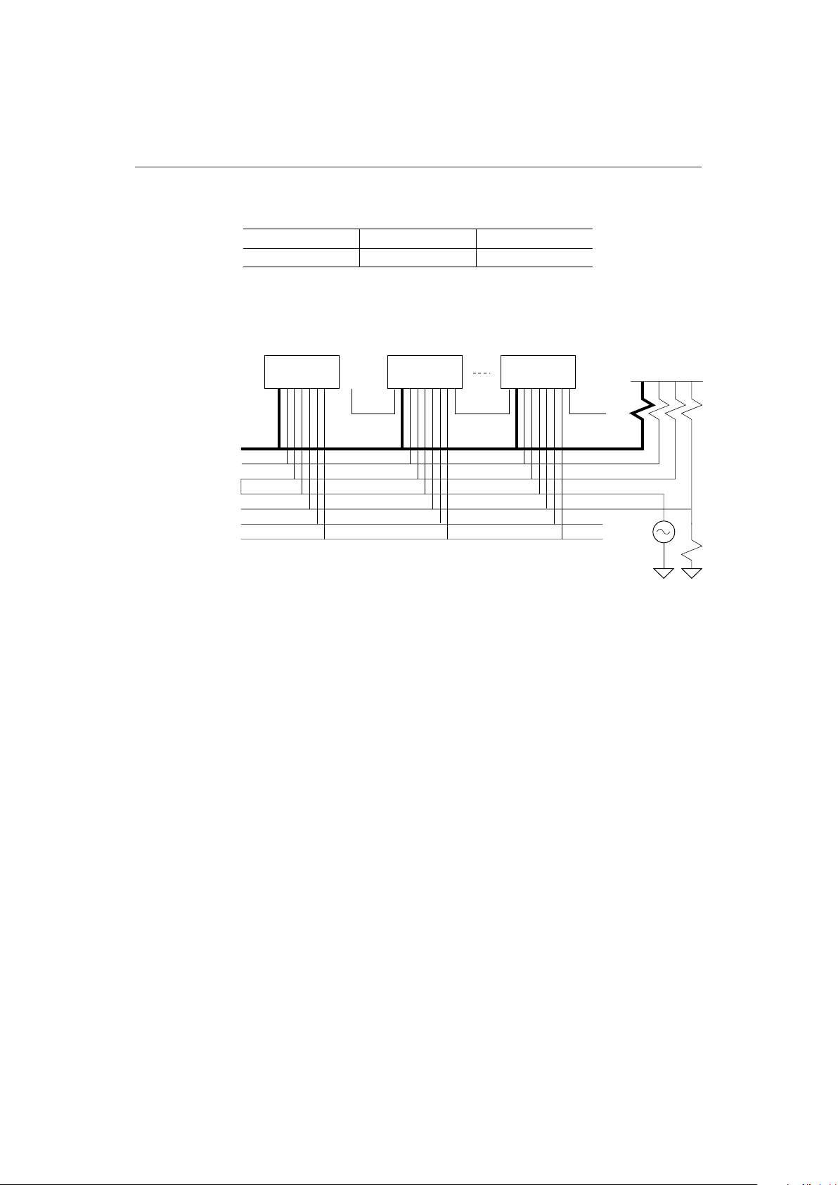
Fig. 2 Controller and RDRAMs Connect to Terminated Transmission Lines
RAMBUS SYSTEM OVERVIEW
A typical Rambus memory system has three main elements: the Rambus Controller, the channel, and
the RDRAMs. The logical representation of this is shown in Fig. 2.
The Rambus channel is a high-speed, byte-wide, synchronous bus used to connect Rambus devices
together. The channel carries all address, data, and control information to and from devices. Transfer
of data on the Rambus channel is managed through the use of a high level block-oriented protocol.
BusData [8:0]
BusCtrl, BusEnable
ClkFromMaster
ClkToMaster
Vref
Gnd, GndA
Vdd, VddA
Controller RDRAM 1 RDRAM n
V
term
SIn
Rambus Channel = 9 bits every 2 ns
Vdd
SOut
NC
SInSOut
Page 4
MSM5718B70 ¡ Semiconductor
4
a b c d e f g h
Byte h
Byte g
Byte f
Byte e
Byte d
Byte c
Byte b
Bank 1 Bank 2
Sense Amp Cache page 1 Sense Amp Cache page 2
Address Comparators
Registers
Bank 3 Bank 4
Bank 5 Bank 6
Bank 7 Bank 8
RDRAM 4
RDRAM 3
RDRAM 2
RDRAM 1
Clocking
Rambus Channel
9 bits every 2 ns
Rambus Interface Cell
Macrocell in embedded array and standard cell libraries
Converts Rambus channel small swing signals to ASICcore-compatible CMOS levels
Converts 9 bits every 2 ns to 72 bits (X2) every 16 ns
Contains PLLs
•
•
•
•
Byte a
The Rambus channel has thirteen high-speed Rambus Signaling Logic (RSL) I/O signals that are
used to transfer information at 2 nanosecond intervals. These signals use low voltage swings (logic
0 = 2.25 V, logic 1 = 1.55 V) to achieve high bus speeds. Two TTL level signals are used for initialization
and powerdown operation. Fourteen signals supply power and DC voltage references to the
RDRAM, and the remaining pins are No Connects (reserved for future expansion).
The Rambus interface is implemented on both master and slave devices. Rambus masters (ASIC
devices, memory controllers, graphics engines, peripheral chips, or microprocessors) are the only
devices capable of generating transaction requests. RDRAMs are slave devices and can respond to
requests from master devices.
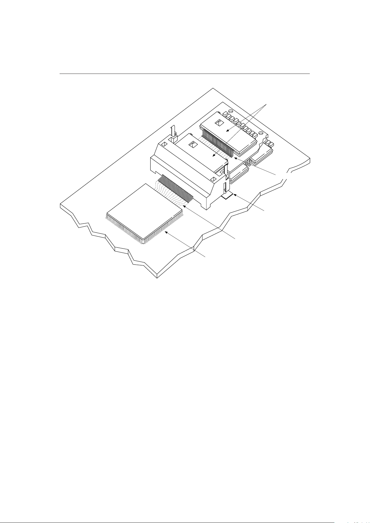
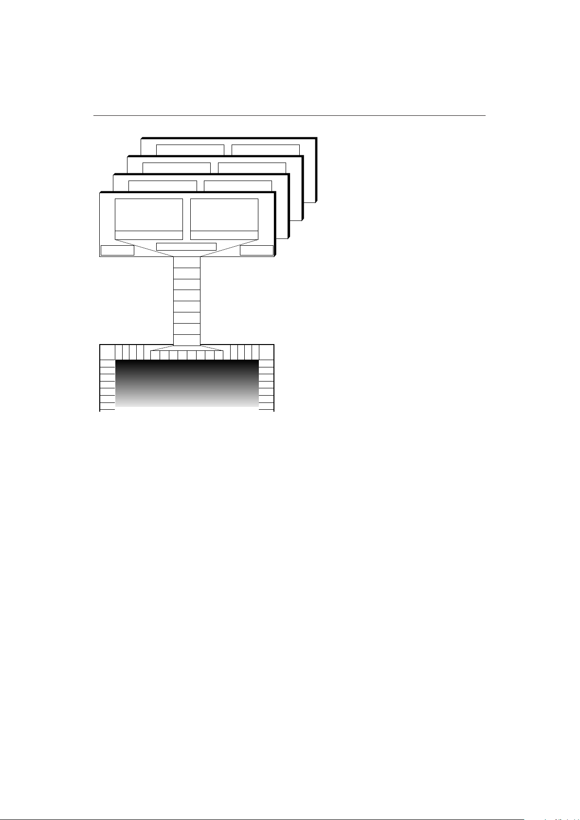
Fig. 1 shows a typical physical implementation of a Rambus system. It includes a controller ASIC
that acts as the Channel master and a base set of RDRAMs soldered directly to the board. An
RSocket™ is included on the Channel for memory upgrade using RModule™ expansion cards.
Fig. 3 Data Transfer on the Rambus Channel
Page 5

¡ Semiconductor MSM5718B70
5
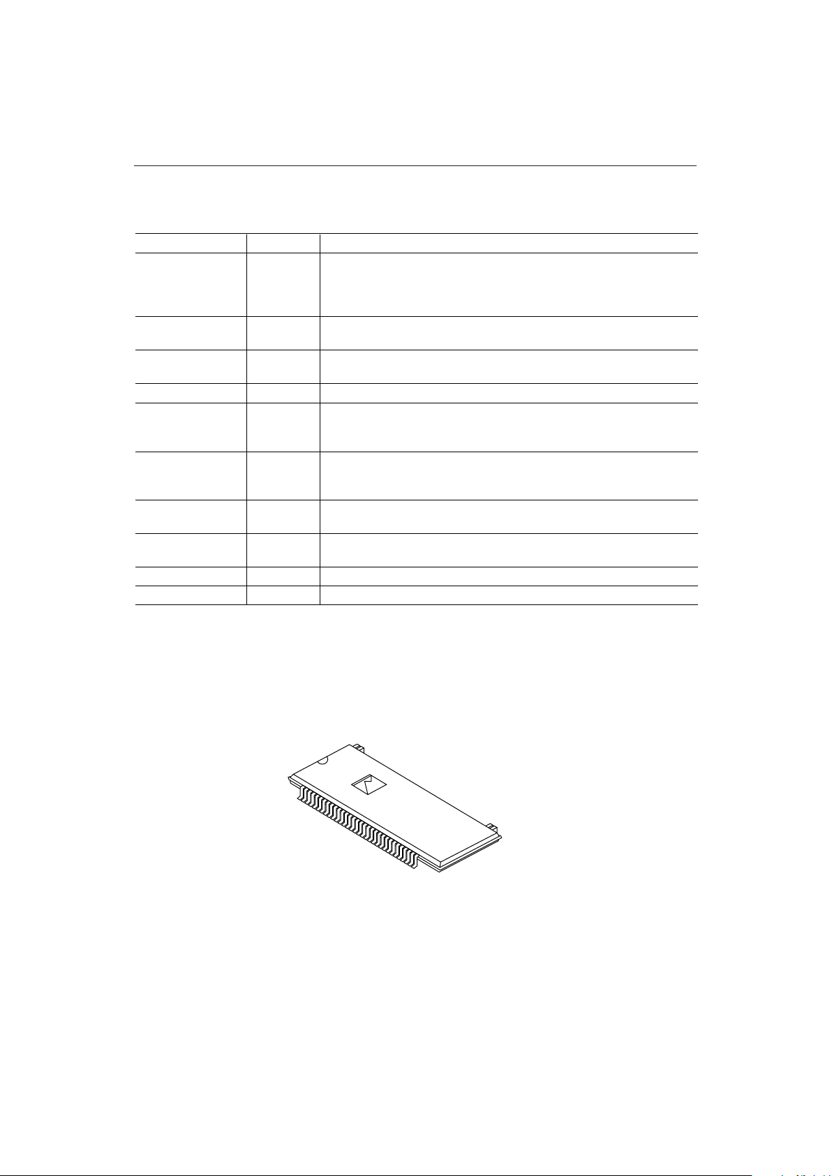
RDRAM PACKAGES AND PINOUTS
RDRAMs are available in horizontal surface mount plastic package (SHP).
The package has 32 signal pins and four mechanical pins that provide support for the device. The
mechanical pins are located on the opposite side from the signal leads in the SHP.
V
DD
1
Gnd
2
BusData8 3
Gnd 4
BusData7
5
(NC) 6
BusEnable
7
V
DD
8
BusData6 9
Gnd
10
BusData5 11
V
DDA
12
RxClk 13
GndA 14
TxClk
15
V
DD
16
BusData4
17
Gnd 18
BusCtrl 19
SIn
20
V
REF
21
SOut
22
BusData3 23
Gnd 24
BusData2
25
(NC) 26
BusData1 27
Gnd
28
BusData0 29
(NC)
30
Gnd 31
V
DD
32
Fig. 4 SHP Pin Numbering
Page 6
MSM5718B70 ¡ Semiconductor
6
Table 2 Pin Descriptions
Signal lines for request, write data, and read data packets. The request
packet contains the address, operation codes, and the count of the bytes
to be transferred. These are low-swing active-low signals referenced to
Vref.
Signal I/O Description
BusData [8-0] I/O
Receive clock. Incoming request and write data packets are aligned to
this clock. This is a low-swing active-low signal referenced to Vref.
RxClk I
Transmit clock. Outgoing acknowledge and read data packets are aligned
with this clock. This is a low-swing active-low signal referenced to Vref.
TxClk I
Logic threshold reference voltage for low swing signals.
Vref I
Control signal to frame packets transmit part of the operation code to
acknowledge requests, and to interrupt (terminate) pending transactions.
This is a low-swing active-low signal referenced to Vref.
BusCtrl I/O
Control signal to manage the operating modes of the RDRAMs and to
transfer column addresses for random-access (non-sequential) transactions.
This is a low-swing active-low signal referenced to Vref.
BusEnable I
+3.3V power supply. VddA is a separate analog supply for clock recovery
in the RDRAM.
Vdd, VddA
Circuit ground. GndA is a separate analog ground for clock generation in
the RDRAM.
Gnd, GndA
Initialization daisy chain input. TTL levels. Active high.
SIn I
Initialization daisy chain output. TTL levels. Active high.
SOut O
Pin 1
Pin 32
Mechanical
Pins
Mechanical
Pins
Fig. 5 SHP Package
Page 7
¡ Semiconductor MSM5718B70
7
PROTOCOL
The transaction protocol used in Rambus systems is built from several types of information packets.
These include the request, acknowledge, serial mode, and data packets.
Request Packet
A master device initiates a transaction by generating a six-byte request packet containing address,
control, and byte count information as shown in Fig. 6. The Op and OpX fields in the Request packet
contain a command that is used to instruct the RDRAM which operation is being requested. A
summary of these commands is shown in Table 3.
Start Op[0]
Bus-
Ctrl
Bus-
Enable
BusData (8:0)
Adr[9:2]
Op[1] Op[3] Adr[17:10]
OpX[1] Adr[26:18]
Op[2] Adr[35:27]
OpX[0] Count[6, 4, 2]ReqUnimp[5:4] ReqUnimp[3:0]
Count[7, 5, 3]ReqUnimp[8:6] Count[1:0] Adr[1:0]
—
—
—
—
—
—
[0]
even
[0]
odd
[1]
even
[1]
odd
[2]
even
[2]
odd
Time
Clock Cycle Number
Fig. 6 Request Packet
1
Note: 1. A — in this diagram signifies that this pin is not used by this packet. If it is not used
by another packet, it is pulled to a logic zero value.
Page 8

MSM5718B70 ¡ Semiconductor
8
Table 3 Command Summary
Op[3:0] OpX[1:0] Name Description
Read sequential data from memory space.
0000 00 Rseq
Read random-access (non-sequential) data from memory space.0000 01 Rnsq
Write sequential data to memory space with no per-bit mask application.0100 00 WseqNpb
Write sequential data to memory space with data-per-bit masking. Static
bit masks are supplied by the MDReg while write data is supplied in the
data packet.
0100 01 WseqDpb
Write sequential data to memory space with mask-per-bit masking. Both
write data and dynamic bit masks are supplied in the data packet.
0100 10 WseqBpb
Write sequential data to memory space with mask-per-bit masking. Static
write data is supplied by the MDReg while dynamic bit masks are supplied
in the data packet.
0100 11 WseqMpb
Read data from register space.
0110 00 Rreg
Write data to register space.
0111 00 Wreg
Write random-access (non-sequential) data to memory space with no perbit mask application.
1000 00 WnsqNpb
Write random-access (non-sequential) data to memory space with maskper-bit masking. Both write data and dynamic bit masks are supplied in
the data packet.
1000 10 WnsqBpb
Write random-access (non-sequential) data to memory space with maskper-bit masking. Static write data is supplied by the MDReg while dynamic
bit masks are supplied in the data packet.
1000 11 WnsqMpb
Write random-access (non-sequential) data to memory space with byte
masking and no per-bit mask application. Both byte masks and write data
are supplied in the data packet.
1100 00 WbnsNpb
Write random-access (non-sequential) data to memory space with byte
masking and data-per-bit masking. Static bit masks are supplied by the
MDReg while byte masks and write data are supplied in the data packets.
1100 01 WbnsDpb
Write random-access (non-sequential) data to memory space with byte
masking and mask-per-bit masking. Static write data is supplied by the
MDReg while byte masks and dynamic bit masks are supplied in the data
packets.
1100 11 WbnsMpb
Broadcast write to register space of all responding devices with no acknowledge permitted.
1111 WregB00
Write random-access (non-sequential) data to memory space with data-perbit masking. Static bit masks are supplied by the MDReg while write data is
supplied in the data packet.
01 WnsqDpb
1000
Page 9
¡ Semiconductor MSM5718B70
9
Acknowledge Packet
Each RDRAM monitors the channel for a request to access its assigned memory range. The device
matching the address range requested then drives an acknowledge packet back to the master.
Ack[0]
Bus-
Ctrl
Bus-
Enable
BusData (8:0)
Ack[1]
—
—
[0]
even
[0]
odd
Time
Clock Cycle Number
—
—
The Ack[1:0] field in the Acknowledge packet carries the RDRAM's response to the request. If the
RDRAM is able to complete the operation as requested, it returns an okay response. If the RDRAM
is unable to complete the operation as requested, it returns a negative acknowledge response (Nack).
The encoding of the Ack[1:0] bits is shown in Table 4.
Table 4 Ack[1:0] Encodings
In response to an acknowledged command, the RDRAM either drives a data packet back to the
master in the case of a read, or accepts a data packet from the master in the case of a write. Fig. 8 shows
an example of 16 byte read and write transactions. The actual timing from the end of a request packet
to data and acknowledge packets is adjustable through RDRAM register settings.
Ack [1:0] Name Description
Indicates passive acceptance of the request (WregB), or indicates that the addressed
device did not respond (all other commands).
00
Non-
existent
Indicates that the request was accepted by the addressed (responding) device.
01 Okay
Indicates that the request could not be accepted because the state of the responding
device prevented an access at the fixed timing slot.
10 Nack
This should not be returned by this responding device. Initiating devices will, when
presented with this combination, have an undefined response.
11 Ack3
Fig. 7 Acknowledge Packet
1
Note: 1. A — in this diagram signifies that this pin is not used by this packet. If it is not used
by another packet, it is pulled to a logic zero value.
Page 10
MSM5718B70 ¡ Semiconductor
10
1t
CYCLE
3t
CYCLE
7t
CYCLE
3t
CYCLE
Read Request Read DataAck
1t
CYCLE
Ack
Write Request Write Data
Fig. 8 Sample 16-Byte Read and Write Transactions
Page 11
¡ Semiconductor MSM5718B70
11
Serial Address Packet
The non-sequential (Random Access) commands specify the eight column address bits needed to
access random octbytes within the open page. These address bits are provided using a Serial Address
packet.
SAdr
[1][3]
Bus-
Ctrl
Bus-
Enable
BusData (8:0)
—
—
[4]
even
Clock Cycle Number
—
—
SAdr
[1][4]
[4]
odd
SAdr
[1][5]
—
—
[5]
even
—
—
SAdr
[1][6]
[5]
odd
SAdr
[1][7]
—
—
[6]
even
—
—
SAdr
[1][8]
[6]
odd
SAdr
[1][9]
—
—
[7]
even
—
—
SAdr
[1][10]
[7]
odd
SAdr
[n][3]
—
—
[4*n]
even
—
—
SAdr
[n][4]
[4*n]
odd
SAdr
[n][5]
—
—
[4*n+1]
even
—
—
SAdr
[n][6]
[4*n+1]
odd
SAdr
[n][7]
—
—
[4*n+2]
even
—
—
SAdr
[n][8]
[4*n+2]
odd
SAdr
[n][9]
—
—
[4*n+3]
even
—
—
SAdr
[n][10]
[4*n+3]
odd
Time
Fig. 9 Serial Address Packet Format
1
Note: 1. A — in this diagram signifies that this pin is not used by this packet. If it is not used
by another packet, it is pulled to a logic zero value.
Page 12
MSM5718B70 ¡ Semiconductor
12
Serial Control Packet
The protocol also allows the channel master to issue an early termination instruction for a memory
read or write transaction. This is done using a Serial Control packet.
SCtrl
[0]
Bus-
Ctrl
Bus-
Enable
BusData (8:0)
—
—
[0]
even
Clock Cycle Number
—
—
SCtrl
[1]
[0]
odd
SCtrl
[2]
—
—
[1]
even
—
—
SCtrl
[3]
[1]
odd
SCtrl
[4]
—
—
[2]
even
—
—
SCtrl
[5]
[2]
odd
SCtrl
[6]
—
—
[3]
even
—
—
SCtrl
[7]
[3]
odd
Time
The value of the Serial Control field specifies whether the instruction should continue or terminate.
This is shown in the table below.
Table 5 Serial Control Field
Serial Control Field Description Value
SCtrl[7:0] Continue 00000000
SCtrl[7:0] Terminate 00100000
Fig. 10 Serial Control Packet Format
1
Note: 1. A — in this diagram signifies that this pin is not used by this packet. If it is not used
by another packet, it is pulled to a logic zero value.
Page 13

¡ Semiconductor MSM5718B70
13
Fig. 11 Sample 32-Byte Read Miss and Read Hit Transactions
Serial Mode Packet
Serial Mode Packets are used to instruct the RDRAM to perform a operating mode change. A Serial
Mode Packet is simply a pulse on the BusEnable line.
1t
CYCLE
3t
CYCLE
19t
CYCLE
3t
CYCLE
7t
CYCLE
Read Request
(Miss)
Nack AckRead Request
(Hit)
Read Data
SMode
[0]
Bus-
Ctrl
Bus-
Enable
BusData (8:0)
—
—
[0]
even
Clock Cycle Number
—
—
SMode
[1]
[0]
odd
Time
RDRAM OVERVIEW
The figure on the next page is a block diagram of the RDRAM device. The Rambus channel interface
consists of a clock generator, a receiver, and a transmitter. The clock generator uses the external clock
signals RxClk and TxClk (tapped off the channel traces ClockFromMaster and ClockToMaster) and
creates the internal signals RClk and TClk. These are used by the receiver and transmitter,
respectively, to transfer a bit every 2 nanoseconds on each wire between the RDRAM and the master
device. The receiver and transmitter blocks also contain multiplexing and storage hardware to
permit the internal RDRAM data paths to operate at the slower clock rate (but equivalent bandwidth)
of eight bytes transferred every 15 or 16 nanoseconds (four clock cycles).
The RDRAM also contains control logic and configuration registers. The registers are read and
written using special register space commands and control various aspects of RDRAM operation as
described on page 19.
The remaining logic consists of a standard DRAM memory core and row sense amplifier caches.
Fig. 12 Serial Mode Packet
1
Note: 1.
A — in this diagram signifies that this pin is not used by this packet. If it is not used
by another packet, it is pulled to a logic zero value.
Page 14

MSM5718B70 ¡ Semiconductor
14
Request, SMode, SAdr, SCtrl WriteData[7:0][8:0] ReadData[7:0][8:0]Ack[1:0]
Receiver TransmitterClock Generator
11
11RxClk TxClk
RClk TClk
11
Op[3:0]
OpX[1:0]
Adr[2:0]
Count[7:0]
Start, Close
SMode[1:0]
SAdr[31:1][10:3]
SCtrl[7:0]
8
Adr[10:3]
Adr[35:11]
Address
Mapping
Logic
2537
AddressSelect[3:0][8:0]
Deviceld[3:0][8:0]
DeviceType[3:0][8:0]
Delay[3:0][8:0]
Mode[3:0][8:0]
DeviceManufacture[3:0][8:0]
Row[3:0][8:0]
RefRow[3:0][8:0]
MinInterval[3:0][8:0]
RasInterval[3:0][8:0]
Device Id
Compare
RowAddres
Compare
CoreAddres
Compare
MDReg[7:0][8:0]
72
72
72¥256 RowSenseAmpLatch
72¥256¥512 DRAM Array - Bank 1
72
72
72¥
256
12
CoreBankAddr
CoreRowAddr
9
CoreAccess
CoreRestore
CoreColAddr
8
72¥256 RowSenseAmpLatch
72¥256¥512 DRAM Array - Bank 0
72¥
256
72
Command and
Control Logic
10
10
72 72
Internal Data Bus
1 SIn SOut 1
BusEnable, BusCtrl, BusData[8:0]
ClockToMaster
ClockFromMaster
Rambus Channel
Column
Decoder
Row
Decoder
Fig. 13 RDRAM Block Diagram
Page 15

¡ Semiconductor MSM5718B70
15
RDRAM OPERATION
The RDRAM is composed of two independent banks of memory with each bank storing a full 1
Mbyte of data (see Fig. 13). Each of these banks has a 2KByte open page associated with it that is built
out of sense amplifier arrays. These sense amplifiers hold the last accessed row of their associated
bank in the sense amplifiers. This allows further accesses to the same row of memory to result in page
hits. With the row already stored in the sense amplifiers, subsequent data can be accessed with very
low latency. Each RDRAM added to a system adds two open pages to the memory system helping
to increase hit rates.
A page miss results when a row is accessed that is not currently stored as one of the open pages. When
this happens, the requesting master is sent a NACK Acknowledge packet indicating the requested
row is not yet available. The RDRAM then loads the requested row into the sense amplifiers and
waits for the master to submit a retry of the previous request. Fig. 11 shows an example of a read miss
followed by a read hit for a 32 byte memory read operation.
The amount of time that is needed before the retry can be serviced depends on whether the data in
the open page is clean or dirty. The sense amplifiers act as a "write back" cache in that data written
to the open page is not written into the actual DRAM cells until the page is closed. If the data in an
open page is clean (not previously written) when a new page is requested, the open page does not
need to be written back into the DRAM. If the data in an open page is dirty, then additional time must
be added to the miss retry delay to account for the writeback operation.
ADDRESS MAPPING
Address mapping hardware is provided to increase page hit rates by allowing system designers to
easily perform n-way RDRAM interleaving. In a non-interleaved memory system, contiguous
blocks of addresses follow each other in sequence in one RDRAM, which is then followed by the next
RDRAM.
Using address mapping, adjacent blocks of data (2K or greater) can be separated across several
RDRAMs, and therefore across several open pages. This allows a more optimal mapping of the pages
as caches and creates higher effective page hit rates. In a typical system containing, for example eight
RDRAMs, hit rates could be expected to be as high as 95%. Address mapping is easily adjusted by
writing a control register in each RDRAM.
TRANSACTION CONCURRENCY
Concurrent transactions can be used to optimize RDRAM utilization in high performance applications
by taking advantage of available channel bandwidth during page miss latency periods. When a miss
in one RDRAM takes place, that device will be busy loading a new row into one of its sense amp
caches. The channel and all other RDRAMs will still be available for use. While waiting for the first
RDRAM to finish loading its open page, a transaction to another RDRAM can be initiated. In systems
where memory accesses can be queued, a tansaction can take place for any pending access residing
in a different RDRAM.
Pretouching can be used in systems where certain memory accesses are predictable, such as video
applications. This is done when an application is finished with a particular RDRAM and about to
access a different one. If the next access to an RDRAM is known in advance, a transaction can be first
generated that will cause a row miss and prepare the RDRAM for its next access. When the device
is next accessed, the required row of data will already be loaded in the open page and a page hit will
take place.
Page 16

MSM5718B70 ¡ Semiconductor
16
RANDOM ACCESS MODE
Non-contiguous blocks of memory can be accessed through the use of the read and write nonsequential (Random Access) operations. With these commands multiple eight-byte blocks (octbytes)
of data within an open page can be accessed in any order. To do this, the master device sends a request
packet specifying a non-sequential operation along with the address of the first octbyte to be
accessed. The master device also generates a serial address packet (see Fig. 9) on the BusEnable signal
that specifies the address of the next octbyte. Successive serial address packets continue to specify
new addresses within the open page while data is continuously transferred until the access is
complete.
Random access mode can be used to satisfy the burst order of processors like the Intel™ Pentium™
at full RDRAM bandwidth.
BIT MASKING
Three forms of bit masking are available for memory write operations. These operations are referred
to as data-per-bit (Dpb), mask-per-bit (Mpb), and both-per-bit (Bpb) masking. An eight-byte Mask
Data register (MDReg) within the RDRAM is used to hold the static value of either mask or data
information for these operations. The Mask Data register is an RDRAM internal register that is
written by the Bpb commands, and is used by the Mpb and Dpb commands.
With the Dpb operation, the MDReg is used to hold a static mask that is applied to all octbytes of data
written to the RDRAM core. With the Mpb operation, the MDReg is used to hold an octbyte of static
data that is masked by dynamic bit masks supplied in the data packets before being written to the
RDRAM core.
The Bpb operation requires data packets to alternate between mask and data octbytes. The even data
packets (starting with data packet 0) carry bit masking information which is placed in the MDReg
while the odd data packets carry the data to be masked by the latest contents on the MDReg. This
type of operation is also used to set the MDReg for later use in Dpb and Mpb operations.
Table 6 shows the source of the mask and data for each of the write commands. The first eight
columns show the Wseq and Wnsq sequential and non-sequential (fandom-access) write commands.
Each has four bit mask sub-commands: Npb, Dpb, Mpb, and Bpb.
A write command consists of writing from one to 32 octbytes of data W[31:0]. Each octbyte of data
is masked by an octbyte of bitmask Bit[31:0]; that is, if the bitmask bit is set, then the corresponding
bit of write data is written. If the bitmask bit is clear, then the bit in memory is left unchanged.
Each of the first eight columns of Table 6 shows the source of the up-to-32 octbytes of write data and
bitmask for the eight write commands. The Npb commands use no bitmask at all - effectively the
bitmask is all ones. The Dpb command takes a single octbyte of bitmask from the MDReg and applies
it to all data octbytes that are written. The Dpb command does the reverse and takes a single octbyte
of write data from the MDReg and writes it to each octbyte of memory using a different bitmask from
the data packet. The Bpb commands take an octbyte of bitmask and an octbyte of write data
alternately, and writes them to a single octbyte of memory.
Page 17

¡ Semiconductor MSM5718B70
17
BYTE MASKING
Contiguous byte masking is supported by the WseqNpb command. This command uses the
Adr[2:0] and Count[2:0] fields of the request packet (Fig. 6) to specify the byte masks of the first and
last octbytes of a data packet. The RDRAM also supports a more general form of byte masking called
non-contiguous byte masking. This is available with the Wbns write commands.
As can be seen in column nine of Table 6 for the WbnsNpb command, the first data packet, and every
ninth thereafter, contain byte masking information that is applied to the eight data packets that
follow. This means data packets 0, 9, 19, and 27 (gray boxes in the table) are not written to memory,
but are instead used as byte masks for the eight octbytes of data that follow. This means that the data
packet Data [35:0] may consist of up to 36 octbytes of information: 4 octbytes of byte mask information
and 32 octbytes of data that is actually written to memory.
Each bit of the 64-bit byte mask (one octbyte) controls whether a byte of the following 64 bytes of data
(eight octbytes) is written (one) or not written (zero) to memory.
Static bit masking is also available with non-contiguous byte masking. This is shown in the last two
columns of Table 6 labeled WbnsDpb and WbnsMpb. The WbnsDpb command applies a static bit
held in the MDReg to each octbyte of data W[31:0]. Each bit of the data octbyte is written if the
corresponding bits of both the bitmask and bytemask are a one, and is not written if either is a zero.
The WbnsMpb command applies a different bitmask Bit[31:0] to a static data octbyte held in the
MDReg. Each bit of the data octbyte is written if the corresponding bits of both the bitmask and
bytemask are a one, and is not written if either is a zero.
Figure 14 shows how the bits of each Data[i][[7:0][8:0] octbyte are flow through the wire circuitry as
a function of the operation type. The data W[i][j][8:0] is written if the corresponding Bit[i][j][8:0] and
Byte [i][j] mask bits are set.
Write data to RDRAM
sense amplifier
0
MDreg
mux
10
mux
1
Bpb
Even
octbyte
ByteMask
Data[i][j][8:0]
Wbns
0,9,18,27 octbyte
631
Mpb
DQ[i][j][8:0]
W[i][j][8:0] 9
9
9
Bit[i][j][8:0]
9x Npb
9x Byte[i][j]
9x Wbns
used by other bytes
i = {0, 1, ..., n-1} Data octbyte index
j = {0, 1, ..., 7} Byte index
k = {0, 1, ..., 8} Bit index
9
Fig. 14 MDReg with BitMask and ByteMask Logic - one byte slice
Page 18

MSM5718B70 ¡ Semiconductor
18
Table 6 WriteData, BitMask, and ByteMask Sources
2
Data
Octbyt
Wseq
Npb
Wseq
Dpb
Wseq
Mpb
Wseq
Bpb
Wnsq
Npb
Wnsq
Dpb
Wnsq
Mpb
Wnsq
Bpb
Wbns
Npb
Wbns
Dpb
Wbns
Mpb
MDReg —
Bit
[35:0]W[35:0]
——
Bit
[35:0]W[35:0]
——
Bit
[35:0]
W
[35:0]
Data[0] W[0] Bit[0] W[0] Bit[0] ByteM[7:0]W[0] Bit[0] W[0] Bit[0] ByteM[7:0] ByteM[7:0]
Data[1] W[1] W[0] W[1] W[0] W[0]W[1] Bit[1] W[1] Bit[1] W[0] Bit[0]
Data[2] W[2] Bit[1] W[2] Bit[1] W[1]W[2] Bit[2] W[2] Bit[2] W[1] Bit[1]
Data[3] W[3] W[1] W[3] W[1] W[2]W[3] Bit[3] W[3] Bit[3] W[2] Bit[2]
Data[4] W[4] Bit[2] W[4] Bit[2] W[3]W[4] Bit[4] W[4] Bit[4] W[3] Bit[3]
Data[5] W[5] W[2] W[5] W[2] W[4]W[5] Bit[5] W[5] Bit[5] W[4] Bit[4]
Data[6] W[6] Bit[3] W[6] Bit[3] W[5]W[6] Bit[6] W[6] Bit[6] W[5] Bit[5]
Data[7] W[7] W[3] W[7] W[3] W[6]W[7] Bit[7] W[7] Bit[7] W[6] Bit[6]
Data[8] W[8] Bit[4] W[8] Bit[4] W[7]W[8] Bit[8] W[8] Bit[8] W[7] Bit[7]
Data[9] W[9] W[4] W[9] W[4]
ByteM[15:8]
W[9] Bit[9] W[9] Bit[9]
ByteM[15:8] ByteM[15:8]
Data[10] W[10] Bit[5] W[10] Bit[5] W[8]W[10] Bit[10] W[10] Bit[10] W[8] Bit[8]
Data[11] W[11] W[5] W[11] W[5] W[9]W[11] Bit[11] W[11] Bit[11] W[9] Bit[9]
Data[12] W[12] Bit[6] W[12] Bit[6] W[10]W[12] Bit[12] W[12] Bit[12] W[10] Bit[10]
Data[13] W[13] W[6] W[13] W[6] W[11]W[13] Bit[13] W[13] Bit[13] W[11] Bit[11]
Data[14] W[14] Bit[7] W[14] Bit[7] W[12]W[14] Bit[14] W[14] Bit[14] W[12] Bit[12]
Data[15] W[15] W[7] W[15] W[7] W[13]W[15] Bit[15] W[15] Bit[15] W[13] Bit[13]
Data[16] W[16] Bit[8] W[16] Bit[8] W[14]W[16] Bit[16] W[16] Bit[16] W[14] Bit[14]
Data[17] W[17] W[8] W[17] W[8] W[15]W[17] Bit[17] W[17] Bit[17] W[15] Bit[15]
Data[18] W[18] Bit[9] W[18] Bit[9]
ByteM[23:16]
W[18] Bit[18] W[18] Bit[18]
ByteM[23:16] ByteM[23:16]
Data[19] W[19] W[9] W[19] W[9] W[16]W[19] Bit[19] W[19] Bit[19] W[16] Bit[16]
Data[20] W[20] Bit[10] W[20] Bit[10] W[17]W[20] Bit[20] W[20] Bit[20] W[17] Bit[17]
Data[21] W[21] W[10] W[21] W[10] W[18]W[21] Bit[21] W[21] Bit[21] W[18] Bit[18]
Data[22] W[22] Bit[11] W[22] Bit[11] W[19]W[22] Bit[22] W[22] Bit[22] W[19] Bit[19]
Data[23] W[23] W[11] W[23] W[11] W[20]W[23] Bit[23] W[23] Bit[23] W[20] Bit[20]
Data[24] W[24] Bit[12] W[24] Bit[12] W[21]W[24] Bit[24] W[24] Bit[24] W[21] Bit[21]
Data[25] W[25] W[12] W[25] W[12] W[22]W[25] Bit[25] W[25] Bit[25] W[22] Bit[22]
Data[26] W[26] Bit[13] W[26] Bit[13] W[23]W[26] Bit[26] W[26] Bit[26] W[23] Bit[23]
Data[27] W[27] W[13] W[27] W[13]
ByteM[31:24]
W[27] Bit[27] W[27] Bit[27]
ByteM[31:24] ByteM[31:24]
Data[28] W[28] Bit[14] W[28] Bit[14] W[24]W[28] Bit[28] W[28] Bit[28] W[24] Bit[24]
Data[29] W[29] W[14] W[29] W[14] W[25]W[29] Bit[29] W[29] Bit[29] W[25] Bit[25]
Data[30] W[30] Bit[15] W[30] Bit[15] W[26]W[30] Bit[30] W[30] Bit[30] W[26] Bit[26]
Data[31] W[31] W[15] W[31] W[15] W[27]W[31] Bit[31] W[31] Bit[31] W[27] Bit[27]
Data[32] — — — — W[28]— — — — W[28] Bit[28]
Data[33] — — — — W[29]— — — — W[29] Bit[29]
Data[34] — — — — W[30]— — — — W[30] Bit[30]
Data[35] — — — — W[31]— — — — W[31] Bit[31]
Note: 2. The shaded data packet contains byte masking information that is applied to the eight
data packets that follow.
Page 19

¡ Semiconductor MSM5718B70
19
Byte[0]
8
7 6 5 4 3 2 1 0
Byte[1]
Byte[2]
Byte[3]
ColumnBits
BankBits
Version
RowBits
Type
Bns
DeviceType Register - 0
Bns (Bonus) - 9 (1) bit bytes
ColumnBits - 1011 (number of column addr bits)
1
Read-only register that defines the size and
configuration of an RDRAM.
RowBits - 1001 (number of row addr bits)
2
BankBits - 0001 (number of bank addr bits)
3
–
–
Type - 0000 (RDRAM device)
Version - 0001 (extended architecture)
1. This value specifies the number of bytes per row (1011=11
10
=211=2048 bytes). This is the address range over
which accesses may be made without causing a row miss.
2. This value specifies the number of rows per bank (1001=9
10
=29=512 rows).
3. This value specifies the number of banks per RDRAM (1=1
10
=21=2 banks).
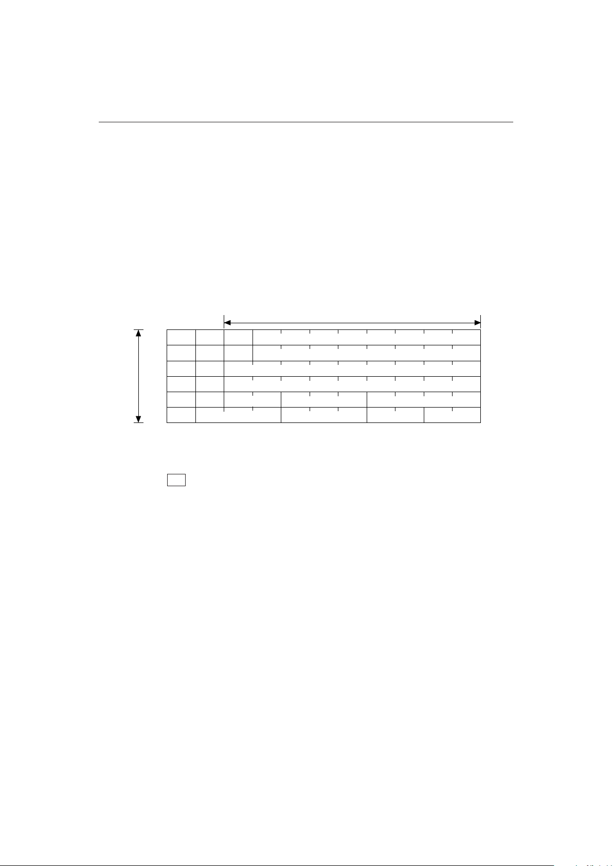
RDRAM REGISTERS
The 18M RDRAM contains ten registers. These are read and written with the Rreg, Wreg, and WregB
commands. They are used to provide configuration information to the RDRAM controller
(DeviceType, MinInterval, and DeviceManufacture), to control device, bank, and row addressing
(DeviceId, AddressSelect, and Row), to control refresh (RefRow), to control RDRAM timing (Delay
and RasInterval), and to control RDRAM operation (Mode). The following table summarizes these
functions:
Table 7 Register Summary
Register Name Reg. # Description
Read-only register that defined the size and configuration of the RDRAM.DeviceType[3:0][8:0] 0
Used to specify the base address for the RDRAM.Deviceld[3:0][8:0] 1
Used to specify CAS timing parameters.Delay[3:0][8:0] 2
Used to initialize the RDRAM and set the IOL output current.Mode[3:0][8:0] 3
Used to specify the next row and bank of the RDRAM to be refreshed.RefRow[3:0][8:0] 5
Used to specify RAS timing parameters.RasInterval[3:0][8:0] 6
Read-only register defining minimum timing parameters for CAS accesses.
MinInterval[3:0][8:0] 7
Used to specify address bit swapping to maximize RDRAM cache hit rate.AddressSelect[3:0][8:0] 8
Read-only register containing a manufacturer code.DeviceManufacturer[3:0][8:0] 9
Used to specify the currently sensed row in each bank.Row[3:0][8:0] 128
The following diagrams show the individual fields of the RDRAM registers. The color of a field
denotes its usage: dark-gray is unimplemented, light-gray is read-only, and white is read-write. The
arrow within each multi-bit field points from the least-significant bit to the most-significant bit. Bit
and byte numbering use little-endien notation.
Fig. 15 Registers
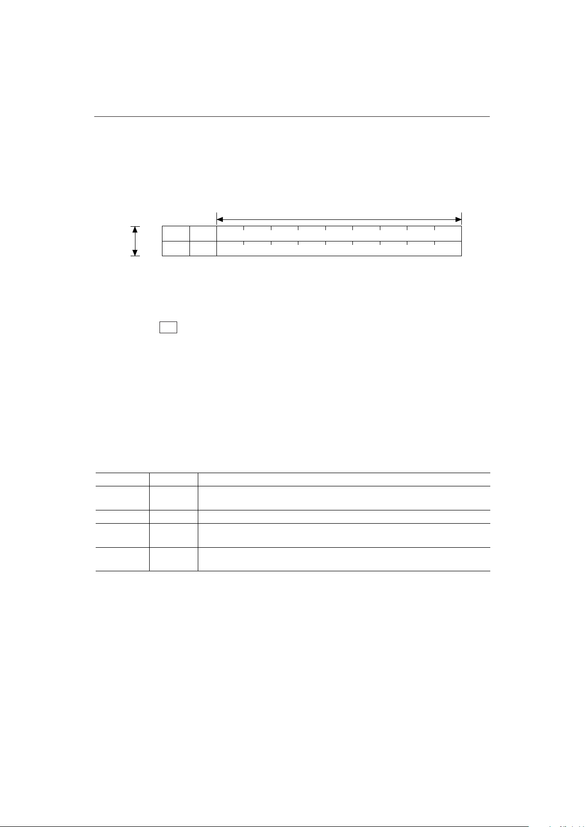
Page 20

MSM5718B70 ¡ Semiconductor
20
Byte[0]
8
7 6 5 4 3 2 1 0
Byte[1]
Byte[2]
Byte[3]
AckWinBits
Delay Register -2
AckWinBits - 011 (Number of AckWinDelay bits)
AckWinDelay - Normally set to 101 (5 busclocks)
Read-write and read-only register to
program the CAS access delays.
ReadBits - 011 (Number of ReadDelay bits)
ReadDelay - Normally set to 111 (7 busclocks)
AckBits - 010 (Number of AckDelay bits)
AckDelay - Normally set to 011 (3 busclocks)
WriteBits - 011 (Number of WriteDelay bits)
WriteDelay - Normally set to 001 (1 busclocks)
AckWinDelay adjusts the size of the acknowledge window. ReadDelay, WriteDelay, and AckDelay adjust the time
from the end of the packet to the start of read data, write data, and the acknowledge packets, respectively.
AckWinDelay
ReadBitsReadDelay
AckBitsAckDelay
WriteBitsWriteDelay
Byte[0]
8
7 6 5 4 3 2 1 0
Byte[1]
Byte[2]
Byte[3]
CE
Mode Register - 3
DE (DevEn) - Selects RDRAM at initialization
AS - Set to one
Read-write register for initializing the RDRAM
and for controlling operating modes.
PL (PwrLng) - Selects powerdown wake-up time
X2 (CCMult) - Set to one.
CE (CCEnable) - Set to one.
–
–
C[5:0] (CCValue) - Specifies I
OL
• 63 = minimum
X2 PL AS DE
C5 C2
C4 C1
C3 C0
0 = maximum
Byte[0]
8
7 6 5 4 3 2 1 0
Byte[1]
Byte[2]
Byte[3]
IdField[35:21]
Deviceld Register - 1
IdField [35:21] - Compared to Adr[35:21] of
request packet to select RDRAM.
Read-write register for setting the base
address of the RDRAM.
–
–
–
–
–
–
Page 21

¡ Semiconductor MSM5718B70
21
Byte[0]
8
7 6 5 4 3 2 1 0
Byte[1]
Byte[2]
Byte[3]
MinInterval Register - 7
MinWriteDelay - 0001
(minimum WriteDelay of RDRAM)
Read-only register (configuration info)
and write-only register (special control).
MinReadDelay - 0111
(minimum ReadDelay of RDRAM)
MinAckDelay - 0011
(minimum AckDelay of RDRAM)
SpecFunc - Performs SetRR burst
refresh and SetPD powerdown entry
SpecFunc
MinAckDly
MinReadDly
MinWriteDly
MinWriteDelay, MinReadDelay, and MinAckDelay specify the minimum number of cycles allowed between a request
packet and a write data, read data, and acknowledge packet, respectively. SpecFunc is a write-only field that is used
to initiate a SetRR burst refresh or to place the RDRAM into powerdown mode.
Byte[0]
8
7 6 5 4 3 2 1 0
Byte[1]
Byte[2]
Byte[3]
RowPrecharge
RasInterval Register - 6
RowPrecharge - Set the precharge interval
(Program to 01000)
Read-write register to program the RAS access
intervals. Note that fields are in bit-reversed order.
RowSense - Set the sense interval
(Program to 01100)
RowImpRestore - Set the implicit restore interval
(Program to 10010)
RowExpRestore - Set the explicit restore interval
(Program to 00100)
RowSense
RowImpRestore
RowExpRestore
Byte[0]
8
7 6 5 4 3 2 1 0
Byte[1]
Byte[2]
Byte[3]
RowField
RefRow Register - 5
RowField - Next row to be refreshed by SetRR
–
Read-write register for setting the next
row refreshed by SetRR burst refresh.
BankField - Next bank to be refreshed by SetRR
–
–
–
–
–
Bank
Field
Page 22

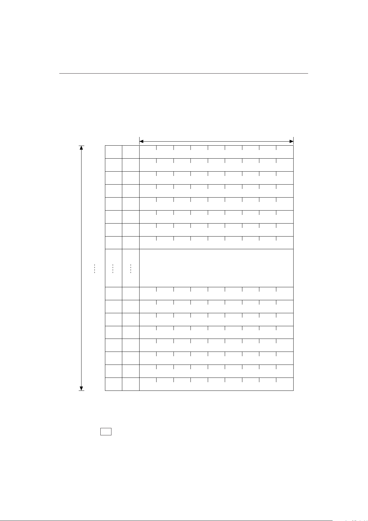
MSM5718B70 ¡ Semiconductor
22
Byte[0]
8
7 6 5 4 3 2 1 0
Byte[1]
Byte[2]
Byte[3]
SwapField
AddressSelect Register - 8
SwapField - Each bit swaps a pair of
bits from Adr[28:20] and Adr[19:11]
Read-write register for swapping subfields of the
Adr field of request packet. This maximizes the
row hit rate for many applications.
–
–
–
–
–
–
Byte[0]
8
7 6 5 4 3 2 1 0
Byte[1]
Byte[2]
Byte[3]
SensedRow[0]
Row Register - 128
SensedRow[0] - Address of currently
sensed row of bank 0.
Read-write register with address of currentlysensed row in each bank of RDRAM.
–
–
SensedRow[1] - Address of currently
sensed row of bank 1.
–
–
SensedRow[1]
Byte[0]
8
7 6 5 4 3 2 1 0
Byte[1]
Byte[2]
Byte[3]
ManufactureCode
DeviceManufacture Register - 9
ManufactureCode - See RDRAM Design Guide
for more information.
Read-only register with configuration
information for RDRAM.
–
–
Manufacturer - Contains code specifying
the manufacturing company.
–
–
ManufactureCode
Manufacturer
Manufacturer
Page 23

¡ Semiconductor MSM5718B70
23
REFRESH
The RDRAM is a dynamic device, and the memory array must be refreshed every 17 ms (t
REF
). The
RDRAM includes all of the logic necessary to support three refresh modes to support this need.
These refresh modes are:
• Manual Refresh:
The Rambus channel master uses a register write transaction (SetRR) to initiate a single burst
refresh of four rows.
• Touching:
A single row is refreshed each time that a read or write request is made to that row in the RDRAM.
• PowerDown Mode Refresh:
A single row is refreshed with each pulse on the SIn/SOut pins.
When the RDRAM is in PowerDown mode, it can be refreshed by passing a periodic pulse at a
frequency of 60.2 kHz or greater through the SIn/SOut pins. This minimum frequency is equal to
1024/t
REF
.
OPERATING MODES
The RDRAM has three operating modes; Active, Standby and PowerDown. The three modes are
distinguished by two factors, their power consumption, and the time that it will take the RDRAM
to service a request from that mode.
The control logic within the RDRAM includes a counter that counts Serial Mode packets. It takes
a specific number of packets to cause the RDRAM to transition from a low-power mode to the Active
state. This counter is active in all three operating modes.
In Active mode, the RDRAM is active and ready to immediately service a request packet. Power
consumption is also highest in Active mode.
An RDRAM automatically transitions to Standby mode at the end of a transaction. While in this low
power state, each RDRAM monitors the BusEnable signal for a serial mode packet while ignoring
other activity on the remaining channel signals. The channel master sends a serial mode packet to
bring all RDRAMs temporarily out of Standby and into Active mode so they can respond to a
request packet. Once the request packet is acknowledged, all of the RDRAMs return to Standby
mode with the exception of the one responding to the request. That device returns to Standby mode
once the read or write operation is complete.
Unlike conventional DRAM memory systems where each device in an entire bank of memory must
be kept active and consumes power through an entire access, Rambus memory systems use only one
active device while all others remain in a lower power state.
Power consumption may be greatly reduced by using the PowerDown mode. This mode is entered
manually by setting the Special Function bit
SetPD
in the MinInterval register. Entering this mode
causes the device to write back and precharge both cache lines, disable the internal clock generator,
and disable most DC current sources. The BusEnable receiver is kept active to detect serial mode
packets used to exit powerdown mode. The only significant power consumption in powerdown
mode is due to refresh.
Page 24

MSM5718B70 ¡ Semiconductor
24
Since the RDRAM's internal clocks are disabled while in powerdown mode, refresh must be
maintained manually by the master device. This is done by supplying a low frequency square wave
on the SIn TTL signal. This propagates through each RDRAM and is used to initiate asynchronous
refresh operations in each device.
Each RDRAM may be placed in either low or high threshold powerdown mode. Threshold refers
to the number of serial mode packets required to wake up the RDRAM. A low threshold requires
relatively few serial mode packets while a high threshold requires a larger number. The actual power
dissipation is identical in both modes.
An example of where these modes are used is in a portable computer application, as shown below.
The sleep mode is implemented by placing a majority of the RDRAMs in high threshold powerdown
while the RDRAM that contains the frame buffer is placed in low threshold powerdown. This
permits screen refresh to take place without powering up the entire memory system.
Standby Mode
(reduced power dissipation)
Reset Mode
(place device in known state)
PowerDown Mode
(minimum power dissipation)
Active Mode
(ready to receive request)
Transaction Processing States
PowerOn
Count < t
MODEAR,MIN
Count ≥ t
MODEPA {1/0}, MIN
Count ≥ t
MODEDELAY, MAX
Write SetPD in MinInterval registerCount ≥ t
MODEAR,MIN
Count ≥ t
MODESA, MIN
Count = # SMode Packets
BusCtrl
even
= 1
(Start Bit)
Transaction complete
Fig. 16 RDRAM Operating Modes
Page 25

¡ Semiconductor MSM5718B70
25
INITIALIZATION
The channel master resets the RDRAM devices on the channel by asserting the BusEnable signal for
T
MODEAR, MIN
clock cycles. After the RDRAM has been reset, the base address and register space
registers revert to their default values. Because the default address of all devices is zero until
initialization is complete, individual devices cannot be addressed from the channel, although the
devices can and will respond to broadcast commands.
In a typical system application, the SIn pin of the first RDRAM is tied to VDD (refer to Figure 2). The
SIn pin of the next RDRAM is connected to the SOut pin of the first RDRAM, and so on. SOut of the
last device is left unconnected. An RDRAM will not respond to a write command (other than a
broadcast write) until its SIn pin is set to 1. Note that if PowerDown mode is to be used by the
application, it must be possible to connect a 60.2 kHz pulse source to SIn of the first RDRAM to
provide refresh.
To start the initialization sequence, The RAC cell in the controller is reset, its DLL is allowed to lock,
and its current control register is loaded. Next, the RDRAMs are put into Reset state by asserting the
BusEnable wire for t
MODEAR, MIN
cycles. The t
LOCK, RESET
interval is observed to allow the RDRAM
DLLs to lock.
After the RDRAMs have been placed in Reset state, broadcast writes are made to all control registers
needing values different from their Reset values. Next, SIn is asserted high on the first RDRAM in
the chain. This enables it. The channel master then writes the desired device address to the DeviceID
register and sets the
DevEn
bit. This asserts the SOut pin (and the SIn pin on the next device in the
chain) to 1. Before proceeding to the next RDRAM, these additional steps are taken on the current
RDRAM:
1. Current control calibration. The value written into the CCValue field of the Mode register is
finetuned to maximize signal margin. This calibration process must take place before the
controller performs any register or memory reads or any acknowledge responses.
2. Check read-only fields of control registers. This confirms which type of Base RDRAMs are
present. This also provides an indication of when the end of the channel is reached.
3. Set the RasInterval register fields.
4. Touch the RDRAM with eight successive memory read transactions. This settles timing circuitry.
This process continues until all of the RDRAMs have been initialized. When these steps have been
completed for every device in the chain, all of the RDRAM devices will have unique, contiguous
DeviceID values, and will have
DevEn
bits set.
Page 26
MSM5718B70 ¡ Semiconductor
26
ABSOLUTE MAXIMUM RATINGS
The following table represents stress ratings only, and functional operation at the maximum ratings
is not guaranteed. Extended exposure to the maximum ratings may affect device reliability.
Although these devices contain protective circuitry to resist damage from static electric discharge,
always take precautions to avoid high static voltages or electric fields.
V
I,ABS
V
DD,MAX
+0.5
Symbol Parameter Unit
Voltage applied to any RSL pin with respect to Gnd
Max.Min.
–0.5 V
V
I,TTL,ABS
VDD+0.5Voltage applied to any TTL pin with respect to Gnd –0.5 V
V
DD,ABS
V
DD,MAX
+1.0Voltage on VDD with respect to Gnd –0.5 V
T
J,ABS
125Junction temperature under bias –55 °C
T
STORE
125Storage temperature –55 °C
THERMAL PARAMETERS
T
J
100
Symbol Parameter and Conditions Unit
Junction operating temperature
Max.Min.
0°C
Q
JC
5Junction-to-Case thermal resistance — °C/Watt
T
C
90Package surface temperature — °C
CAPACITANCE
C
I
2
Symbol Parameter and Conditions Unit
Low-swing input parasitic capacitance
Max.Min.
—pF
C
I,TTL
8TTL input parasitic capacitance — pF
POWER CONSUMPTION
Powerdown 20a/20b/30
c
Mode Description Unit
Device shut down
Max.Min.
—mW
Standby
330a/340b/360
c
Device inactive — mW
Active
0.9a/0.95b/1.0
c
Device evaluating request packet — W
Read 1.4
a
/1.5b/1.6
c
Data being transferred from device
(@Burst Length = 256)
—W
Write 1.3
a
/1.4b/1.5
c
Data being transferred to device
(@Burst Length = 256)
—W
(Ta = 0˚C to 70˚C)
Notes:
a. 500 MHz rank
b. 533 MHz rank
c. 600 MHz rank
Page 27

¡ Semiconductor MSM5718B70
27
RECOMMENDED ELECTRICAL CONDITIONS
V
DD, VDDA
3.45
Symbol Parameter and Conditions Unit
Supply voltage
Max.Min.
3.15 V
V
REF
VDD–0.8Reference voltage 1.9 V
V
IL
V
REF
–0.35
Input low voltage
V
REF
–0.8 V
V
IH
V
REF
+0.8
Input high voltage
V
REF
+0.35 V
V
IL,TTL
0.8
TTL input low voltage
–0.5 V
V
IH,TTL
VDD+0.5TTL input high voltage 1.8 V
(Ta = 0˚C to 70˚C)
ELECTRICAL CHARACTERISTICS
I
REF
10
Symbol Parameter and Conditions Unit
V
REF
CURRENT @
V
REF,MAX
Max.Min.
–10 mA
I
OH
10Output high current @ (0 £ V
OUT
£ VDD) –10 mA
I
OL,0
4.0
Output low current @ V
OUT
=1.6 V @ C[5:0]=111111 (6310)
a
0.0 mA
I
OL,20
22.0
Output low current @ V
OUT
=1.6 V @ C[5:0]=110001 (4910)a18.0 mA
I
OL,40
44.0
Output low current @ V
OUT
=1.6 V @ C[5:0]=011111 (3110)a36.0 mA
I
I,TTL
10.0TTL input leakage current @ (0 £ V
I,TTL
£ VDD) –10.0 mA
V
OL,TTL
0.4TTL output voltage @ I
OL,TTL
=1.0 mA 0.0 V
V
OH,TTL
V
DD
TTL output high voltage @ I
OH,TTL
= –0.25 mA 2.0 V
(Ta = 0˚C to 70˚C)
Note:
a. This is the value written into the C[5:0] field of the Mode register. Values of IOL in between the
I
OL,0
, I
OL,20
, and I
OL,40
values are produced by interpolating C[5:0] to intermediate values. For
example, C[5:0] = 101000 (4010) produces an IOL in the range of 27.0 to 33.0 mA.
Page 28

MSM5718B70 ¡ Semiconductor
28
RECOMMENDED TIMING CONDITIONS
tCR, t
CF
0.8
Symbol Parameter Unit
TxClk and RxClk input rise and fall times
Max.Min.
0.3 ns
t
CYCLE
4.5TxClk and RxClk cycle times
3.33/3.75/4.0
ns
Transport time per bit per pin (this timing interval is
synthesized by the RDRAM's internal clock generator)
0.5 (2.25 ns @
t
CYCLE
= 4.5ns)
0.5 (2 ns @
t
CYCLE
= 4ns)
t
TICK
t
CYCLE
tCH, t
CL
55%TxClk and RxClk high and low times 45% t
CYCLE
t
TR
0.7TxClk-RxClk differential 0 t
CYCLE
tDR, t
DF
0.6Data/Control input rise and fall times 0.3 ns
t
QR
, t
QF
0.5Data/Control output rise and fall times 0.3 ns
t
S
—Data/Control-to-RxClk setup time 0.35 ns
t
H
—RxClk-to-Data/Control hold time 0.35 ns
RDRAM internal clock generator lock time from Reset
mode
750 (3 ms @
t
CYCLE
= 4ns)
—t
LOCK,RESET
t
CYCLE
t
REF
17Refresh interval — ms
RDRAM internal clock generator lock time from PowerUp
mode
750 (3 ms @
t
CYCLE
= 4ns)
—t
LOCK,POWERUP
t
CYCLE
(Ta = 0˚C to 70˚C)
Page 29

¡ Semiconductor MSM5718B70
29
TIMING CHARACTERISTICS
t
PIS
25
Symbol Parameter Unit
SIn-to-SOut propagation delay @ C
LOAD,TTL = 40 pF
Max.Min.
1ns
t
Q
TClk-to-Data/Control output time ns
(Ta = 0˚C to 70˚C)
– 0.4
t
CYCLE
4
+ 0.4
t
CYCLE
4
RAMBUS CHANNEL TIMING
The next table shows important timings on the Rambus channel for common operations. All timings
are from the point of view of the channel master, and thus have the bus overhead delay of 4 ns per
bus transversal included where appropriate.
Symbol Parameter UnitMax.Min.
t
RESPONSE
9
a
Start of request packet to start of acknowledge packet 6
a
t
CYCLE
t
READHIT
17
a
Start of request packet to start of read data packet for
row hit (Okay)
10
a
t
CYCLE
t
WRITEHIT
11
a
Start of request packet to start of write data packet for
row hit (Okay)
4
a
t
CYCLE
t
RETRYSENSED
CLEAN (no restore)
—
Start of request packet for row miss (Nack) to start of
request packet for row hit (Okay). The previous row had
not been written
22
b
t
CYCLE
t
RETRYSENSED
DIRTY (restore)
—
Start of request packet for row miss (Nack) to start of
request packet for row hit (Okay). The previous row had
been written
30
b
t
CYCLE
t
RETRYREFRESH
CLEAN (no restore)
—
Start of request that performs a burst refresh (SetRR)
until the start of a request that will not have a Nack
acknowledge due to the pending refresh. The previously
sensed row had not been written
209 t
CYCLE
t
RETRYREFRESH
DIRTY (restore)
—
Start of request that performs a burst refresh (SetRR)
until the start of a request that will not have a Nack
acknowledge due to the pending refresh. The previously
sensed row had been written
217 t
CYCLE
(Ta = 0˚C to 70˚C)
Page 30

MSM5718B70 ¡ Semiconductor
30
t
READBURST32
—
Symbol Parameter Unit
Start of request packet to end of 32 byte read data packet
for row hit (Okay)
Max.Min.
26
c
t
CYCLE
t
READBURST256
—
Start of request packet to end of 256 byte read data
packet for row hit (Okay)
138 t
CYCLE
t
WRITEBURST32
—
Start of request packet to end of 32 byte write data
packet for row hit (Okay)
20
d
t
CYCLE
t
WRITEBURST256
—
Start of request packet to end of 256 byte write data
packet for row hit (Okay)
132 t
CYCLE
End of request packet to beginning of read data packett
READDELAY
147
a
t
CYCLE
End of request packet to beginning of write data packett
WRITEDELAY
81
a
t
CYCLE
t
ACKDELAY
6
End of request packet to beginning of acknowledge
packet
3
a
t
CYCLE
Window in which an acknowledge packet will be sentt
ACKWINDELAY
125
a
t
CYCLE
t
SERIALREADOFFSET
13
Delay from the beginning of a serial address packet or
serial control packet to the beginning of the corresponding read data subpacket
13 t
CYCLE
t
POSTMEMWRITEDELAY
—
Delay from the beginning of a serial address packet or
serial control packet to the beginning of the corresponding write data subpacket
2t
CYCLE
Delay from the end of the current memory space transaction to the beginning of the next memory space transaction
t
SERIALWRITEOFFSET
55t
CYCLE
t
POSTREGWRITEDELAY
—4t
CYCLE
Delay from the end of the current register space transaction to the beginning of the next register space transaction
Offset from the beginning of SMode packet to request
packet for standby to active transaction
t
MODEOFFSET
44t
CYCLE
Number of SMode packets to cause a transition from
StandbyMode to ActiveMode
t
MODESA
41t
CYCLE
Number of SMode packets to cause a transition from
PowerDownMode[0] to ActiveMode
t
MODEPA[0]
—20 t
CYCLE
Number of SMode packets to cause a transition from
PowerDownMode[1] to ActiveMode
t
MODEPA[1]
—176 t
CYCLE
Number of SMode packets necessary to cause a
transition from ActiveState to ResetState
t
MODEAR
—254 t
CYCLE
Delay time after a transaction is complete for the RDRAM
to enter the StandbyState
t
MODEDELAY
20—t
CYCLE
Offset from the beginning of the request of the current
transaction to the beginning of the request packet of
the next transaction.
t
INTERREQUEST
—6t
CYCLE
Time that a row may remained sensed within a bank.t
RAS, MAX
125— ms
Notes:
a. Programmable - All RDRAMS will operate across the full programming range.
b. Minimum at t
CYCLE,MIN
. The delay is programmable to give equivalent timings at longer t
CYCLE
.
c. Calculated with t
READHIT,MIN
d. Calculated with t
WRITEHIT,MIN
Page 31

¡ Semiconductor MSM5718B70
31
RISE/FALL TIMING
V
RxClk
V
TxClk
80%
V
IH,MIN
20%
V
IL,MAX
t
CF
t
CR
V
Data,in
V
Control,in
80%
V
IH,MIN
20%
V
IL,MAX
t
DF
t
DR
V
Data,out
V
Control,out
80%
V
OH,MIN
20%
V
OL,MAX
t
QF
t
QR
Where:
V
OH,MIN
= V
TERM,MIN
V
OL,MAX
= V
TERM
- ZO* (I
OL,MAX
* programmed value)
CLOCK TIMING
V
TxClk
Logic 0, V
IH
V
REF
Logic 1, V
IL
t
TR
Logic 0, V
IH
V
REF
Logic 1, V
IL
V
RxClk
t
CL
t
CH
t
CYCLE
t
CYCLE
t
CL
t
CH
Page 32

MSM5718B70 ¡ Semiconductor
32
RECEIVE DATA TIMING
Logic 0, V
IH
V
REF
Logic 1, V
IL
V
RxClk
t
CYCLE
t
TICK
(even)
t
TICK
(odd)
Logic 0, V
IH
V
REF
Logic 1, V
IL
tSt
H
tSt
H
V
Data,in
V
Control,in
* t
TICK
is defined as one-half t
CYCLE
.
TRANSMIT DATA TIMING
Logic 0, V
IH
V
REF
Logic 1, V
IL
V
TxClk
t
CYCLE
t
TICK
(even)
t
TICK
(odd)
Logic 0, V
IH
V
REF
Logic 1, V
IL
t
Q,MAX
V
Data,out
V
Control,out
* t
TICK
is defined as one-half t
CYCLE
.
t
Q,MAX
t
Q,MIN
t
Q,MIN
Page 33

¡ Semiconductor MSM5718B70
33
SERIAL CONFIGURATION PIN TIMING
Logic 1
V
SW,TTL
Logic 0
Logic 1
V
SW,TTL
Logic 0
Logic 1
V
SW,TTL
Logic 0
V
SIn
V
SOut
V
SIn
t
PIO,MAX
t
PIO,MIN
t
SL
t
SH
t
SCYCLE
V
SW,TTL
=1.5 V
STANDBY MODE TO ACTIVE MODE TIMING
RxClk
BusData
BusEn
BusCtrl
t
CYCLE
t
MODEOFFSET,MIN
11
t
MODESA,MIN
t
ACKDELAY
Request
Ack
Standby Mode Active Mode
Request Request
t
INTERREQUEST, MIN
Page 34

MSM5718B70 ¡ Semiconductor
34
RESET TIMING
RxClk
BusData
BusEn
BusCtrl
t
CYCLE
Request
t
LOCK,RESET,MIN
11
t
ACKDELAY
Request
Ack
Reset Mode Active Mode
t
MODEAR,MIN
READ HIT TIMING DIAGRAM
RxClk
BusData
BusEn
BusCtrl
t
CYCLE
t
READHIT
t
READDELAY
Request Data Data(n-3) Data(n-2) Data(n-1) Data(n)
t
SERIALREADOFFSET
SAdr(1) SAdr(2) SAdr(3) SAdr(n)
t
ACKDELAY
t
RESPONSE
Ack(1:0
)
SCtrl(n+1)
Page 35

¡ Semiconductor MSM5718B70
35
WRITE HIT TIMING DIAGRAM
RxClk
BusData
BusEn
BusCtrl
t
CYCLE
t
WRITEHIT
Request Data(0) Data(n-1) Data(n)
t
WRITEDELAY
t
SERIALWRITEOFFSET
SAdr(1) SAdr(2) SAdr(n)
t
ACKDELAY
t
RESPONSE
Ack(1:0)
SCtrl(n+1)
READ MISS TIMING DIAGRAM
RxClk
BusData
BusEn
BusCtrl
t
CYCLE
Request
t
READHIT
t
RESPONSE
Ack(1:0) = Nack
Request Data(0)
t
RESPONSE
Ack(1:0) = Ack
t
RETRYSENSEDCLEAN
or
t
RETRYSENSEDDIRTY
Page 36

MSM5718B70 ¡ Semiconductor
36
WRITE MISS TIMING DIAGRAM
RxClk
BusData
BusEn
BusCtrl
t
CYCLE
Request
t
WRITEHIT
t
RESPONSE
Ack(1:0) = Nack
Request Data(1)
t
RESPONSE
Ack(1:0) = Ack
t
RETRYSENSEDCLEAN
or t
RETRYSENSEDDIRTY
Data(0)
REGISTER READ TIMING DIAGRAM
RxClk
BusData
BusEn
BusCtrl
t
CYCLE
Request
t
READDELAY
t
ACKDELAY
Data
Request Ack
Page 37

¡ Semiconductor MSM5718B70
37
REGISTER WRITE TIMING DIAGRAM
RxClk
BusData
BusEn
BusCtrl
t
CYCLE
Request
t
WRITEDELAY
t
ACKDELAY
Data
Ack
Request
Request Request
t
POSTREGWRITEDELAY
MANUAL REFRESH USING SETRR
RxClk
BusData
BusEn
BusCtrl
t
CYCLE
Request
t
WRITEDELAY
t
ACKDELAY
Data
Ack
t
RETRYREFRESH
Request
REFRESH TIMING FOR POWERDOWN MODE USING SIN, SOUT
SIn
t
REF
/1024
Page 38

MSM5718B70 ¡ Semiconductor
38
POWER DOWN TIMING (REGISTER WRITE)
RxClk
BusData
BusEn
BusCtrl
t
CYCLE
Request
t
ACKDELAY
Data
AckRequest
Active Mode PowerDown Mode
POWER UP TIMING
RxClk
BusData
BusEn
BusCtrl
t
CYCLE
Request
t
ACKDELAY
Ack
PowerDown Mode Active Mode
Request
t
MODEPA[0/1],MINtLOCK,POWERUP,MIN
11
Page 39

¡ Semiconductor MSM5718B70
39
MECHANICAL DRAWINGS
The RDRAM is available in a horizontal surface mount plastic package. Dimensions for the
horizontal surface mount plastic package are shown below.
Pkg D
Pkg A
Pin 1
Pin e
Pin 32
Pkg E
Fig. 17 SHP-32 Package
Fig. 18 SHP-32 Footprint
The next figure shows the footprint of the SHP-32 package. Plane R-R is the electrical reference plane
of the device on the center line of the SMT pads.
Pad 0
All pins on 0.65 horizontal grid
Pin e
Sup D1
Pin e
1
Pad b3 Pad l1
32
R-R
Page 40

MSM5718B70 ¡ Semiconductor
40
This table summarizes the values of the package and footprint dimensions.
Table 8 SHP-32 Package Dimensions
Symbol Parameter Min. Typ. Unit
— 0.65 mmPin e Pin pitch
24.9 25.0 mmPkg D Package width
12.8 13.0 mmPkg A Package total height
—— mmPkg E Package thickness
0.30 — mmPad b3 SMT pad width
1.2 — mmPad l1 SMT pad length
— 22.75 mmSup D1 Support pad outer pitch
— 12.5 mmPad O SMT pad offset
Max.
—
25.1
13.2
1.75
0.40
1.4
—
—
 Loading...