

Page 1
1/30
Semiconductor
M SM56V16800F
2-Bank ´ 1,048,576 Word ´ 8 Bit SYNCHRONOUS DYNAMIC RAM
DESCRIPTION
The MSM56V16800F is a 2-Bank ´ 1,048,576-word ´ 8 bit Synchronous dynamic RAM, fabricated in OKI’s
CMOS silicon-gate process technology. The device operates at 3.3V. The inputs and outputs are LVTTL
compatible.
FEATURES
· Silicon gate , quadruple polysilicon CMOS , 1-transistor memory cell
· 2-bank ´ 1,048,576-word ´ 8bit configuration
· 3.3V power supply ± 0.3V tolerance
· Input : LVTTL compatible
· Output : LVTTL compatible
· Refresh : 4096 cycles/64 ms
· Programmable data transfer mode
- CAS Latency (1,2,3)
- Burst Length (1,2,4,8,Full page)
- Data scramble (sequential , interleave)
· CBR auto-refresh, Self-refresh capability
· Package:
44-pin 400mil plastic TSOP (Type II) (TSOPII44-P-400-0.80-K) (Product : MSM56V16800F-xxTS-K)
xx : indicates speed rank.
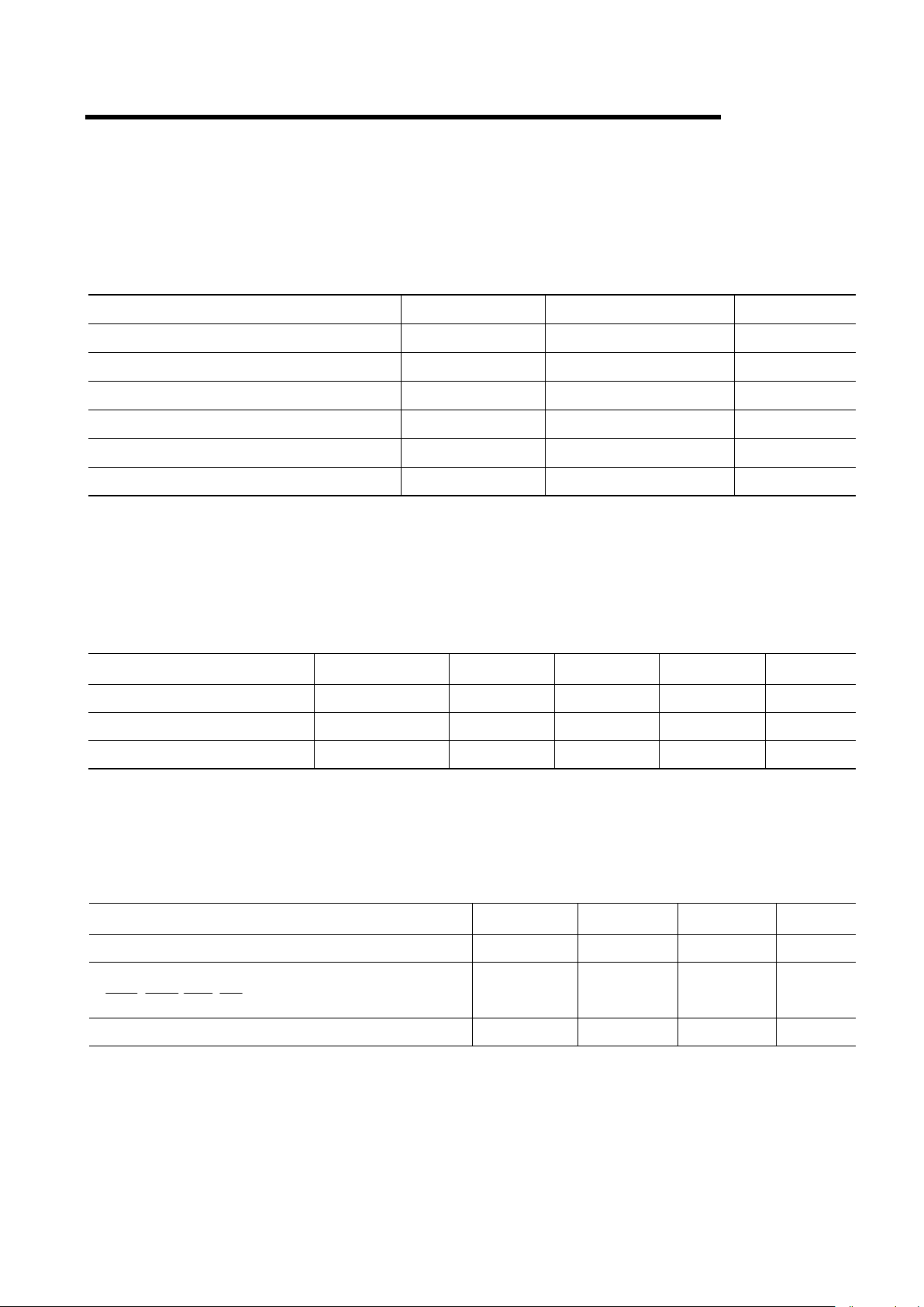
PRODUCT FAMILY
Access Time (Max.)
Family
Max.
Frequency
t
AC2
t
AC3
MSM56V16800F-8A
125MHz
6ns 6ns
MSM56V16800F-8 125MHz 9ns 6ns
MSM56V16800F-10 100MHz 9ns 9ns
This version : Dec.1999
Page 2
MSM56V16800F
2/30
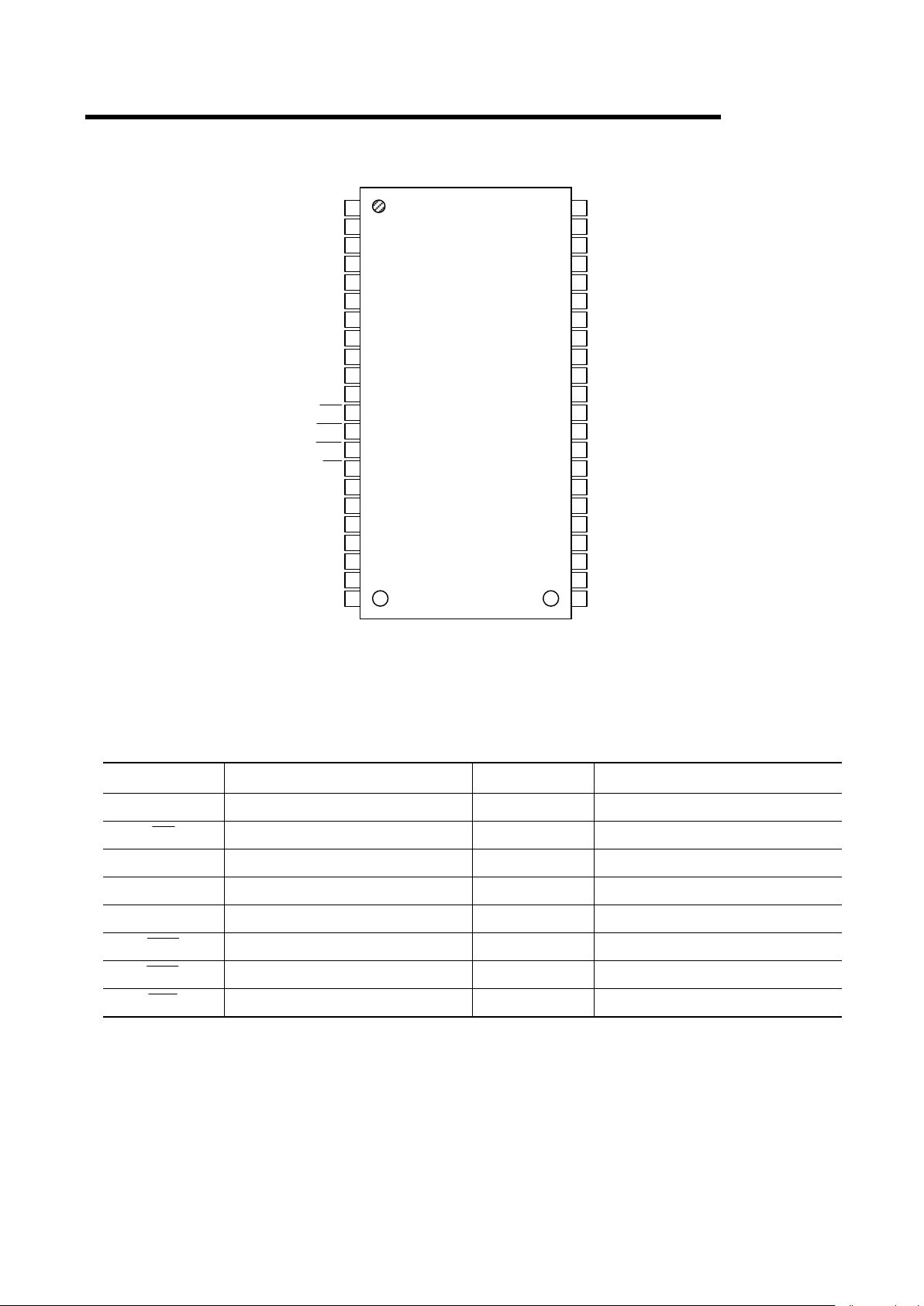
PIN CONFIGRATION (TOP VIEW)
Pin Name Function Pin Name Function
CLK System Clock DQM Data Input/Output Mask
CS Chip Select DQi Data Input/Output
CKE Clock Enable
V
CC
Power Supply (3.3V)
A0–A10 Address
V
SS
Ground (0V)
A11 Bank Select Address
V
CC
Q
Data Output Power Supply (3.3V)
RAS Row Address Strobe
V
SS
Q
Data Output Ground (0V)
CAS Column Address Strobe NC No Connection
WE Write Enable
Note: T he same power supply voltage must be provided to every VCC pin and VCCQ pin.
The same GND voltage level must be provided to every V
SS
pin and VSSQ pin.
44-Pin Plastic TSOP (II)
(K Type)
1
2
3
4
5
9
10
11
12
13
42
41
40
39
38
DQ1
DQ2
DQ3
V
CC
V
SS
DQ8
DQ7
NC NC
DQM
A9
6
7
8
14
15
RAS
DQ4
19
20
21
22 23
A0
A1
A2
A3
A11
16
17
18
24
25
CS
WE
A10
CAS
44
43
DQ6
DQ5
37
36
32
31
30
29
28 A8
A7
A6
A5
A4
35
34
33
CLK
CKE
NC
27
26
V
SS
V
CC
NC
V
CC
(Q)
V
SS
(Q) VSS(Q)
V
CC
(Q)
NC
V
SS
(Q)
V
CC
(Q)
V
SS
(Q)
V
CC
(Q)
Page 3
MSM56V16800F
3/30
PIN DESCRIPTION
CLK Fetches all inputs at the “H” edge.
CS
Disables or enables device operation by asserting or deactivating all inputs except CLK, CKE,
UDQM and LDQM.
CKE
Masks system clock to deactivate the subsequent CLK operation.
If CKE is deactivated, system clock will be masked so that the subsequent CLK operation is
deactivated. CKE should be asserted at least one cycle prior to a new command.
Address
Row & column multiplexed.
Row address : RA0 – RA10
Column Address : CA0 – CA8
A11
Slects bank to be activated during row address latch time and s elects bank for prec harge and
read/write during column address latch time. A11=”L” : Bank A, A11=”H” : Bank B
RAS
CAS
WE
Functionality depends on the combination. For details, see the function truth table.
DQM
Masks the read data of two clocks later when DQM is set “H” at the “H” edge of the clock
signal. Masks the write data of the s ame clock when DQM is set “H” at the “ H” edge of the
clock signal.
DQi Data inputs/outputs are multiplexed on the same pin.
Page 4
MSM56V16800F
4/30
BLOCK DIAGRAM
Timing
Register
Column
Decoders
Sense
Amplifiers
DQ1
- DQ8
RAS
CAS
A0 - A11
Progra-
ming
Register
Bank
Controller
Latency
& Burst
Controller
Internal
Col.
Address
Counter
I/O
Controller
Column
Address
Buffers
Internal
Row
Address
Counter
Row
Address
Buffers
8
Row
Decoders
Row
Decoders
12
Word
Drivers
Word
Drivers
8Mb
Memory
Cells
8Mb
Memory
Cells
Read
Data
Register
Output
Buffers
Column
Decoders
Sense
Amplifiers
Input
Data
Register
Input
Buffers
CKE
CL
K
CS
WE
DQM
A11
9
12
8
88
8
8
9
Page 5
MSM56V16800F
5/30
ELECTRICAL CHARACTERISTICS
Absolute Maximum Ratings
(Voltages referenced to VSS)
Parameter Symbol Rating Unit
Voltage on Any Pin Relative to V
SS
VIN, V
OUT
-0.5 to VCC + 0.5
V
V
CC
Supply Voltage VCC, VCCQ
-0.5 to 4.6
V
Storage Temperature
T
stg
-55 to 150
°C
Power Dissipation
P
D
*
600 mW
Short Circuit Current
I
OS
50 mA
Operating Temperature
T
opr
0 to 70 °C
*: Ta = 25°C
Recommended Operating Conditions
(Voltages referenced to VSS = 0V)
Parameter Symbol Min. Typ. Max. Unit
Power Supply Voltage
V
CC
,
VCCQ
3.0 3.3 3.6 V
Input High Voltage
V
IH
2.0
¾
V
CC
+ 0.2
V
Input Low Voltage
V
IL
-0.3 ¾
0.8 V
Capacitance
(VCC = 1.4V, Ta = 25°C, f=1MHz)
Parameter Symbol Min. Max. Unit
Input Capacitance (CLK)
C
CLK
2.5 4 pF
Input Capacitance
(RAS, CAS, WE, CS, CKE, DQM, A0-A11)
C
IN
2.5 5 pF
Input/Output Capacitance (DQ1-DQ8)
C
OUT
46.5pF
Page 6

MSM56V16800F
6/30
DC Characteristics
MSM56V16800F
Condition
8A 8 10
Parameter Symbol
Bank CKE Others Min Max Min Max Min Max
Unit Note
Output High
Voltage
V
OH
¾¾
I
OH
= -2.0mA
2.4
¾
2.4
¾
2.4
¾
V
Output Low
Voltage
V
OL
¾¾
I
OL
= 2.0mA
¾
0.4
¾
0.4
¾
0.4 V
Input Leakage
Current
I
LI
¾¾ ¾-10
10
-10
10
-10
10 µA
Input Leakage
Current
I
LO
¾¾ ¾-10
10
-10
10
-10
10 µA
I
CC1
One Bank
Active
CKE³V
IH
tCC=min.
t
RC
=min.
No Burst
¾
70
¾
70
¾
60 mA 1,2
Average power
supply current
(Operating)
I
CC1D
Both Banks
Active
CKE³V
IH
tCC=min.
t
RC
=min.
t
RRD
=min.
No Burst
¾
105
¾
105
¾
85 mA 1,2
Power supply
current (Standby)
I
CC2
Both Banks
Precharge
CKE³V
IH
tCC=min.
¾
35
¾
35
¾
30 mA 3
Average power
supply current
(Clock Suspension)
I
CC3S
Both Banks
Active
CKE£V
IL
tCC=min.
¾
3
¾
3
¾
3mA2
Average power
supply current
(Active Standby )
I
CC3
One Bank
Active
CKE³V
IH
tCC=min.
¾
40
¾
40
¾
35 mA 3
Power supply
current (Burst)
I
CC4
Both Banks
Active
CKE³V
IH
tCC=min.
¾
95
¾
90
¾
80 mA 1,2
Power supply
current
(Auto-Refresh)
I
CC5
One Bank
Active
CKE³V
IH
tCC=min.
t
RC
=min.
¾
70
¾
70
¾
60 mA 2
Average power
supply current
(Self-Refresh)
I
CC6
Both Banks
Precharge
CKE£V
IL
tCC=min.
¾
2
¾
2
¾
2mA
Average power
supply current
(Power Down)
I
CC7
Both Banks
Precharge
CKE£V
IL
tCC=min.
¾
2
¾
2
¾
2mA
Notes: 1. Measured with outputs open.
2. The address and data can be changed once or left unchanged during one cycle.
3. The address and data can be changed once or left unchanged during two cycles.
Page 7
MSM56V16800F
7/30
Mode Set Address Keys
CAS Latency Burst Type Burst Length
A6 A5 A4 CL A3 BT A2 A1 A0 BT = 0 BT = 1
0 0 0 Reserved 0 Sequential 0 0 0 1 1
0 0 1 1 1 Interleave 0 0 1 2 2
010 2 010 4 4
011 3 011 8 8
1 0 0 Reserved 1 0 0 Reserved Reserved
1 0 1 Reserved 1 0 1 Reserved Reserved
1 1 0 Reserved 1 1 0 Reserved Reserved
1 1 1 Reserved 1 1 1 Full Page Reserved
Notes: A7, A8, A9, A10 and A11 should stay “L” during mode set cycle.
POWER ON SEQUENCE
1. With inputs in NOP state, turn on the power supply and start the system clock.
2. After the V
CC
voltage has reached the specified level, pause for 200ms or more with the input kept
in NOP state.
3. Issue the precharge all bank command.
4. Apply a CBR auto-refresh eight or more times.
5. Enter the mode register setting command.
Page 8
MSM56V16800F
8/30
AC Characteristic (1/2)
Note 1,2
MSM56V16800F
8A 8 10
Parameter Symbol
Min. Max. Min. Max. Min. Max.
Unit Note
CL = 3 8
¾
8
¾
10
¾
ns
CL = 2 10
¾
12
¾
15
¾
nsClock Cycles Time
CL = 1
t
CC
20
¾
24
¾
30
¾
ns
CL = 3
¾
6
¾
6
¾
9ns3,4
CL = 2
¾
6
¾
9
¾
9ns3,4Access Time from Clock
CL = 1
t
AC
¾
16
¾
22
¾
27 ns 3,4
Clock High Pulse Time
t
CH
3
¾
3
¾
3
¾
ns 4
Clock Low Pulse Time
t
CL
3
¾
3
¾
3
¾
ns 4
Input Setup Time
t
SI
2
¾
2
¾
3
¾
ns
Input Hold Time
t
HI
1
¾
1
¾
1
¾
ns
Output Low Impedance Time
from Clock
t
OLZ
3
¾
3
¾
3ns
Output High Impedance Time
from Clock
t
OHZ
¾
9
¾
9
¾
8ns
Output Hold from Clock
t
OH
3
¾
3
¾
3
¾
ns 3
RAS Cycle Time
t
RC
70
¾
70
¾
90
¾
ns
RAS Precharge Time
t
RP
20
¾
20
¾
30
¾
ns
RAS Active Time
t
RAS
48 10
5
48 10
5
60 10
5
ns
RAS to CAS Delay Time
t
RCD
20
¾
20
¾
30
¾
ns
Write Recovery Time
t
WR
8
¾
8
¾
15
¾
ns
RAS to RAS Bank Active Delay Time
t
RRD
20
¾
20
¾
20
¾
ns
Refresh Time
t
REF
¾
64
¾
64
¾
64 ms
Power-down Exit setup Time
t
PDE
t
SI
+1CLK
¾
t
SI
+1CLK
¾
t
SI
+1CLK
¾
ns
Input Level Transition Time
t
T
¾
3
¾
3
¾
3ns
CAS to CAS Delay Time(Min.)
l
CCD
111Cycle
Clock Disable Time from CKE
l
CKE
111Cycle
Data Output High Impedance Time
from UDQM, LDQM
l
DOZ
222Cycle
Data Input Mask Time from UDQM,
LDQM
l
DOD
000Cycle
Data Input Mask Time from Write
Command
l
DWD
000Cycle
Page 9
MSM56V16800F
9/30
AC Characteristic (2/2)
Note 1,2
MSM56V16800F
8A 8 10
Parameter Symbol
Min. Max Min. Max. Min. Max.
Unit Note
Data Output High Impedance Time
from Precharge Command
l
ROH
CL CL CL Cycle
Active Command Input Time from
Mode Register Set Command Input
(Min.)
l
MRD
333Cycle
Write Command Input Time from
Output
l
OWD
222Cycle
Notes:
1) AC measurements assume that tT = 1ns.
2) The reference level for timing of input signals is 1.4V.
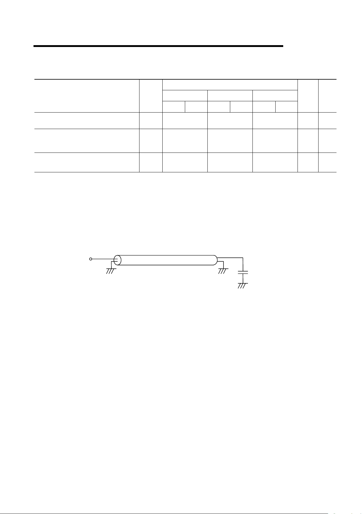
3) Output load.
4) The access time is defined at 1.5V.
5) If tT is longer than 1ns, then the reference level for timing of input signals is VIH and VIL.
Output
Z=50
W
50pF (External Load)
Page 10

MSM56V16800F
10/30
TIMING WAVEFORM
····
Read & Write Cycle (Same Bank) @CAS Latency
====
2, Burst Length
====
4
t
OH
Ra Ca0
t
RP
t
RC
Qa1
RAS
CAS
ADDR
WE
DQM
CLK
CKE
CS
Cb0Rb
A11
RbRa
A10
DQ
Qa0 Q a2 Q a3 Db0 D b1 Db2 D b3
t
AC
t
OHZ
t
WR
Row Active
Read Command Precharge Command
Row Active
Write Command Precharge Command
t
RCD
0 1 2 3 4 5 6 7 8 9 10 11 12 13 14 15 16 17 18 19
Page 11

MSM56V16800F
11/30
····
Single Bit Read-Write-Read Cycle (Same Page) @CAS Latency
====
2, Burst Length
====
4
CLK
CKE
CS
RAS
CAS
ADDR
A11
A10
DQ
WE
DQM
Row Active
0 1 2 3 4 5 6 7 8 9 10 11 12 13 14 15 16 17 18 19
High
t
OLZ
Db
t
SI
Qc
t
HI
Qa
t
OH
Ra
l
OWD
BS BS BSBSBS
Ra CcCbCa
t
OHZ
t
AC
t
HI
t
SI
t
SI
t
HI
t
HI
t
SI
t
SI
t
HI
t
HI
t
SI
I
CCD
t
SI
t
CL
t
CC
t
CH
Read Command
Write Command
Read Command
Precharge Command
Page 12

MSM56V16800F
12/30
*
Notes : 1. When CS is set ”High” at a clock transition from “Low” to ”High”, all inputs ex cept CKE, U DQM and LDQM are
invalid.
2. When issuing an active, read or write command, the bank is selected by A11.
A11 Active, read or write
0 Bank A
1 Bank B
3. The auto precharge function is enabled or disabled by the A10 input when the read or write command is
issued.
A10 A11 Operation
0 0 After the end of burst, bank A holds the idle status.
1 0 After the end of burst, bank A is precharged automatically.
0 1 After the end of burst, bank B holds the idle status.
1 1 After the end of burst, bank B is precharged automatically.
4. When issuing a precharge command, the bank to be precharged is selected by the A10 and A11 inputs.
A10 A11 Operation
0 0 Bank A is precharged.
0 1 Bank B is precharged.
1 X Both banks A and B are precharged.
5. The input data and the write command are latched by the same clock (Write latency = 0).
6. The output is forced to high impedance by (1CLK+t
OHZ
) after UDQM, LDQM entry.
Page 13

MSM56V16800F
13/30
····
Page Read & Write Cycle (Same Bank) @CAS Latency
====
2, Burst Length
====
4
*
Notes: 1. To write data before a burst read ends, DQM should be asserted three cycles prior to the write command to
avoid bus contention.
2. To assert row precharge before a burst write ends, wait tWR after the last write data input.
Input data during the precharge input cycle will be masked internally.
CLK
CKE
CS
RAS
CAS
ADDR
A11
A10
DQ
WE
DQM
Read Command
Read Command
Write Command
Write Command
Precharge Command
Qa0 Qa1 Qb0 Qb1 Dc0 Dc1 Dd0
Cc0 Cd0Ca0 Cb0
t
WR
I
CCD
****
Note 2
****
Note 1
Bank A Active
0 1 2 3 4 5 6 7 8 9 10 11 12 13 14 15 16 17 18 19
l
OWD
High
Page 14

MSM56V16800F
14/30
·
··
· Read & Write Cycle with Auto Precharge @ Burst Length====4
DQ
WE
DQM
Row Active
(A-Bank)
DQ
DQ
A-Bank Precharge Start
CLK
CKE
CS
RAS
CAS
ADDR
A10
A11
0 1 2 3 4 5 6 7 8 9 10 11 12 13 14 15 16 17 18 19
Row Active
(B-Bank)
A Bank Read with
Auto Precharge
B Bank Write with
Auto Precharge
B Bank Precharge
Start Point
A-Bank Precharge Start
A-Bank Precharge Start
High
Ra
t
RRD
Qa0
t
WR
Rb
Ra Rb
Ca Cb
Qa1 Qa2 Q a3 Db0 D b1 Db2 Db3
Db0 Db1 Db2 Db3Qa0 Qa1 Qa2 Qa3
Qa0 Qa1 Qa2 Q a3 D b0 Db1 D b2 Db3
CAS Latency=2
CAS Latency=3
CAS Latency=1
DQM
DQM
Page 15

MSM56V16800F
15/30
x Bank Interleave Random Row Read Cycle @CAS Latency = 2, Burst Length = 4
CLK
CKE
CS
RAS
CAS
ADDR
A11
A10
DQ
WE
DQM
RAa CAa RBb CBb RAc CAc
RAa RBb RAc
QAa0 QAa1 QAa2 QAa3 QBb1 QBb2 QBb3 QBb4 QAc0 QAc1 QAc2 QAc3
Row Active
(A-Bank)
Read Command
(A-Bank)
Precharge Command
(A-Bank)
Row Active
(B-Bank)
Read Command
(B-Bank)
Precharge Command
(B-Bank)
Row Active
(A-Bank)
Read Command
(A-Bank)
t
RRD
t
RC
0 1 2 3 4 5 6 7 8 9 10 11 12 13 14 15 16 17 18 19
High
Page 16

MSM56V16800F
16/30
x Bank Interleave Random Row Write Cycle @CAS Latency = 2, Burst Length =4
CLK
CKE
CS
RAS
CAS
ADDR
A11
A10
DQ
WE
DQM
0 1 2 3 4 5 6 7 8 9 10 11 12 13 14 15 16 17 18 19
RAa CAa RBb CBb RAc CAc
RAa RBb RAc
DAa0 DAa1 DAa2 DAa3
Row Active
(A-Bank)
Write Command
(A-Bank)
Precharge
Command
(A-Bank)
Row Active
(B-Bank)
Write Command
(B-Bank)
Precharge Command
(B-Bank)
Row Active
(A-Bank)
Write Command
(A-Bank)
DBb0 DBb1 DBb2 DBb3 DAc0 DAc1
High
Precharge Command
(A-Bank)
Page 17

MSM56V16800F
17/30
x Bank Interleave Page Read Cycle @CAS Latency = 2, Burst Length =4
Note: 1. CS is ignored when RAS, CAS and WE are high at the same cycle.
CLK
CKE
CS
RAS
CAS
ADDR
A11
A10
DQ
WE
DQM
0 1 2 3 4 5 6 7 8 9 10 11 12 13 14 15 16 17 18 19
RAa CAa RBb CBb CAc CBd CAe
RAa RBb
QAa0 QAa1 QAa2 QAa3 QBb0 QBb1 QBb2 QBb3 QAc0 QAc1 QBd0 QBd1 QAe0 QAe1
*
**
*Note 1
Row Active
(A-Bank)
Read Command
(A-Bank)
Row Active
(B-Bank)
Read Command
(B-Bank)
Precharge Command
(A-Bank)
Read Command
(A-Bank)
Read Command
(A-Bank)
Read Command
(B-Bank)
I
ROH
High
Page 18

MSM56V16800F
18/30
·
··
· Bank Interleave Page Write Cycle @CAS Latency = 2, Burst Length====4
0 1 2 3 4 5 6 7 8 9 10 11 12 13 14 15 16 17 18 19
WE
DQM
Row Active
(A-Bank)
CLK
CKE
CS
RAS
CAS
ADDR
A10
A11
Row Active
(B-Bank)
Write Command
(A-Bank)
Precharge Command
(Both Bank)
High
RAa CAa
RAa RAb
RBb CBd
DQ
DAa3 DBb0 DBb1
DBb2 DBb3 DAc0 DAc1 DBd0
Write Command
(B-Bank)
Write Command
(A-Bank)
Write Command
(B-Bank)
DAa2DAa1DAa0
CAcCBb
Page 19

MSM56V16800F
19/30
· Bank Interleave Random Row Read/Write Cycle @CAS Latency = 2, Burst Length = 4
0 1 2 3 4 5 6 7 8 9 10 11 12 13 14 15 16 17 18 19
CLK
CKE
CS
RAS
CAS
ADDR
A11
A10
DQ
WE
DQM
RAa CAa RBb CBb RAc CAc
RAa RBb RAc
QAa0 QAa1 QAa2 QAa3 QBb0 QBb1 QBb2 QBb3 QAc0 QAc1 QAc2 QAc3
Row Active
(A-Bank)
Read Command
(A-Bank)
Precharge Command
(A-Bank)
Row Active
(B-Bank)
Write Command
(B-Bank)
Row Active
(A-Bank)
Read Command
(A-Bank)
High
Page 20

MSM56V16800F
20/30
· Bank Interleave Page Read/Write Cycle @CAS Latency = 2, Burst Length =4
0 1 2 3 4 5 6 7 8 9 10 11 12 13 14 15 16 17 18 19
CLK
CKE
CS
RAS
CAS
ADDR
A11
A10
DQ
WE
DQM
CAa0 CBb0 CAc0
QAa0 QAa1 QAa2 QAa3
Read Command
(A-Bank)
Write Command
(B-Bank)
Read Command
(A-Bank)
DBb0 DBb1 DBb2 DBb3 QAc0 QAc1
High
QAc2 QAc3
Page 21

MSM56V16800F
21/30
· Clock Suspension & DQM Operation Cycle @CAS Latency = 2, Burst Length =4
*
Notes: 1. When Clock Suspension is asserted, the next clock cycle is ignored.
2. When DQM are asserted, the read data after two clock cycles is masked.
3. When DQM are asserted, the write data in the same clock cycle is masked.
CLK
CKE
CS
RAS
CAS
ADDR
A11
A10
DQ1-8
WE
DQM
Ra Ca Cb Cc
Ra
Qa0 Qa1 Qa2 Qb0 Qb1 Dc0 Dc2
*
**
*Note 1
Row Active
Read Command
CLOCK
Suspension
Read DQM
CLOCK
Suspension
Read Command
Wri te
Command
Read DQM
*
**
*Note 1
*
**
*Note 2
*
**
*Note 3
t
OHZ
Wri t e
DQM
Wri t e
DQM
t
OHZ
0 1 2 3 4 5 6 7 8 9 10 11 12 13 14 15 16 17 18 19
Page 22

MSM56V16800F
22/30
· Read to Write Cycle (Same Bank) @CAS Latency = 2, Burst Length =4
*
Note: 1. In Case CAS latency is 3, READ can be interrupted by WRITE.
The minimum command interval is [burst length + 1] cycles.
DQM must be high at least 3 clocks prior to the write command.
CLK
CKE
CS
RAS
CAS
ADDR
A11
A10
DQ
WE
DQM
Ra Ca0 Cb0
Ra
Db0 Db1
*
**
*Note 1
Row Active
Read Command
Write Command
Precharge Command
t
WR
t
RCD
Db2 Db3
0 1 2 3 4 5 6 7 8 9 10 11 12 13 14 15 16 17 18 19
Da0
Page 23

MSM56V16800F
56263
x Read Interruption by Precharge Command @Burst Length =8
ó
Notes: 1. When the CAS latency = 1, and if row precharge is asserted before a burst read ends, then the read data will not output afte r
the next clock cycle of t he precharge command.
2. When the CAS latency = 2, and if row precharge is asserted before burst read ends, then the read data will not output after
the second clock cycle of the precharge command.
3. When the CAS latency = 3, and if row precharge is asserted before burst read ends, then the read data will not output after
the second clock cycle of the precharge command.
DQ
WE
DQM
DQ
CAS Latency=2
DQ
CAS Latency=3
CLK
CKE
CS
RAS
CAS
ADDR
A11
A10
Ra Ca
ó
óó
óNote 1
Qa0 Qa1
Ra
Qa2
ó
óó
óNote 2
Qa3 Qa4 Qa5
Qa0 Qa1 Qa2 Qa3 Qa4 Qa5
ó
óó
óNote 3
Qa0 Qa1 Qa2 Qa3 Qa4
Row Active Read Command Precharge Command
l
ROH
l
ROH
Qa5
l
ROH
0 1 2 3 4 5 6 7 8 9 10 11 12 13 14 15 16 17 18 19
High
CAS Latency=1
DQM
DQM
Page 24

MSM56V16800F
57263
x
xx
x Burst Stop Command @Burst Length =8
DQ
WE
DQM
DQ
CAS Latency=2
DQ
CAS Latency=3
CLK
CKE
CS
RAS
CAS
ADDR
A11
A10
Ca
Qa0 Qa1
Qa2 Qa3 Qa4
Qa0 Qa1 Qa2 Qa3 Qa4
Qa0 Qa1 Qa2 Qa3 Qa4
CAS Latency=1
Read Command
Cb
Qb0 Qb1 Qb2 Qb3 Qb4
Qb0 Qb1 Qb2 Qb3 Qb4
Qb0 Qb1 Qb2 Qb3 Qb4
Burst Stop
Command
Write Command Burst Stop
Command
0 1 2 3 4 5 6 7 8 9 10 11 12 13 14 15 16 17 18 19
High
DQM
DQM
Page 25

MSM56V16800F
58263
x
xx
x Power Down Mode @CAS Latency = 2, Burst Length =4
ó
Notes: 1. When both banks are in precharge state, and if CKE is set low, then the MSM56V16800F enters pow er-dow n
mode and maintains the mode while CKE is low.
2. To release the circuit from power-down mode, CKE has to be set high for longer than t
PDE (tSI
+ 1CLK).
0 1 2 3 4 5 6 7 8 9 10 11 12 13 14 15 16 17 18 19
CKE
CS
RAS
CAS
ADDR
A11
A10
DQ
Ra Ca
Ra
Qa0 Qa1 Qa2
ó
óó
óNote 2
Power-down
Entry
Row
Active
Power-down
Exit
Precharge
Command
Read Command
Clock
Suspension
Exit
t
SI
CLK
ó
óó
óNote 1
Clock
Suspension
Entry
t
PDE
t
SI
t
SI
t
REF
(min.)
WE
DQM
Page 26

MSM56V16800F
59263
x Self Refresh Cycle
0 1 2
CLK
CKE
CS
RAS
CAS
ADDR
A11
A10
DQ
WE
DQM
Ra
BS
Ra
Self Refresh
Entry
Self Refresh
Exit
Row Active
t
SI
t
RC
Hi - Z
Page 27

MSM56V16800F
5:263
x Mode Register Set Cycle xxxx Auto Refresh Cycle
DQ
CLK
CKE
CS
RAS
CAS
ADDR
WE
DQM
New Command
l
MRD
Auto Refresh
t
RC
MRS Auto Refresh
Key Ra
0 1 2 3 4 5 6 9 10 110 1 2 3 4 5 6 7 8
Hi - Z Hi - Z
High High
Page 28

MSM56V16800F
28/30
FUNCTION TRUTH TABLE (Table 1) (1/2)
Current State1CS RAS CAS WE BA ADDR Action
HXXXX XNOP
LHHHX XNOP
L H H L BA X
ILLEGAL
2
LHLXBACA
ILLEGAL
2
L L H H BA RA Row Active
L L H L BA A10
NOP
4
LLLHX X
Auto-Refresh or Self-Refresh
5
Idle
LLLLLOP CodeMode Register Write
HXXXX XNOP
LHHXX XNOP
LHLHBACA, A10Read
L H L L BA CA, A10 W rite
LLHHBARA
ILLEGAL
2
L L H L BA A10 Precharge
Row Active
LLLXX XILLEGAL
HXXXX XNOP (Continue Row Active after Burst ends)
L H H H X X NOP (Continue Row Active after Burst ends)
L H H L X X Term Burst --> Row Active
L H L H BA CA, A10
Term Burst, start new Burst Read
3
L H L L BA CA, A10
Term Burst, start new Burst Write
3
LLHHBARA
ILLEGAL
2
L L H L BA A10 Term Burst, execute Row Precharge
Read
LLLXX XILLEGAL
HXXXX XNOP (Continue Row Active after Burst ends)
L H H H X X NOP (Continue Row Active after Burst ends)
L H H L X X Term Burst --> Row Active
L H L H BA CA, A10
Term Burst, start new Burst Read
3
L H L L BA CA, A10
Term Burst, start new Burst Write
3
LLHHBARA
ILLEGAL
2
L L H L BA A10
Term Burst, execute Row Precharge
3
Write
LLLXX XILLEGAL
HXXXX XNOP (Continue Burst to End and enter Row Precharge)
L H H H X X NOP (Continue Burst to End and enter Row Precharge)
L H H L BA X
ILLEGAL
2
L H L H BA CA, A10
ILLEGAL
2
L H L L X X ILLEGAL
L L H X BA RA, A10
ILLEGAL
2
Read with
Auto Prechar
g
e
LLLXX XILLEGAL
HXXXX XNOP (Continue Burst to End and enter Row Precharge)
L H H H X X NOP (Continue Burst to End and enter Row Precharge)
L H H L BA X
ILLEGAL
2
L H L H BA CA, A10
ILLEGAL
2
L H L L X X ILLEGAL
L L H X BA RA, A10
ILLEGAL
2
Write with
Auto Prechar
g
e
LLLXX XILLEGAL
Page 29

MSM56V16800F
29/30
FUNCTION TRUTH TABLE (Table 1) (2/2)
Current State1CS RAS CAS WE BA ADDR Action
HXXXX X
NOP --> Idle after t
RP
LHHHX X
NOP --> Idle after t
RP
L H H L BA X
ILLEGAL
2
LHLXBACA
ILLEGAL
2
LLHHBARA
ILLEGAL
2
L L H L BA A10
NOP
4
Precharge
LLLXX XILLEGAL
HXXXX XNOP
LHHHX XNOP
L H H L BA X
ILLEGAL
2
LHLXBACA
ILLEGAL
2
LLHHBARA
ILLEGAL
2
L L H L BA A10
ILLEGAL
2
Write Recovery
LLLXX XILLEGAL
HXXXX X
NOP --> Row Active after t
RCD
LHHHX X
NOP --> Row Active after t
RCD
L H H L BA X
ILLEGAL
2
LHLXBACA
ILLEGAL
2
LLHHBARA
ILLEGAL
2
L L H L BA A10
ILLEGAL
2
Row Active
LLLXX XILLEGAL
HXXXX X
NOP --> Idle after t
RC
LHHXX X
NOP --> Idle after t
RC
L H L X X X ILLEGAL
L L H X X X ILLEGAL
Refresh
LLLXX XILLEGAL
HXXXX XNOP
LHHHX XNOP
L H H L X X ILLEGAL
L H L X X X ILLEGAL
Mode Register
Access
LLXXX XILLEGAL
ABBREVIATIONS
RA = Row Address BA = Bank Address NOP = No OPeration command
CA = Column Address AP = Auto Precharge
*
Notes : 1. All inputs are enabled when CKE is set high for at least 1 cycle prior to the inputs.
2. Illegal to bank in specified state, but may be legal in some cases depending on the state of bank selection.
3. Satisfy the timing of l
CCD
and tWR to prevent bus contention.
4. NOP to bank precharging or in idle state. Precharges activated bank by BA or A10.
5. Illegal if any bank is not idle.
Page 30

MSM56V16800F
30/30
FUNCTION TRUTH TABLE for CKE (Table 2)
Current State (n) CKEn-1 CKEn CS RAS CAS WE ADDR Action
H X X X X X X INVALID
L H H X X X X Exit Self Refresh --> ABI
L H L H H H X Exit Self Refresh --> ABI
L H L H H L X ILLEGAL
L H L H L X X ILLEGAL
L H L L X X X ILLEGAL
Self Refresh
L L X X X X X NOP (Maintain Self Refresh)
H X X X X X X INVALID
L H H X X X X Exit Power Down --> ABI
L H L H H H X Exit Power Down --> ABI
L H L H H L X ILLEGAL
L H L H L X X ILLEGAL
LHLLXXX
ILLEGAL
6
Power Down
L L X X X X X NOP (Continue power down mode)
H H X X X X X Refer to Table 1
H L H X X X X Enter Power Down
H L L H H H X Enter Power Down
H L L H H L X ILLEGAL
H L L H L X X ILLEGAL
H L L L H L X ILLEGAL
H L L L L H X Enter Self Refresh
H L LLLL XILLEGAL
All Banks Idle
6
(ABI)
L L XXXX XNOP
H H X X X X X Refer to Operations in Table 1
H L X X X X X Begin Clock Suspend Next Cycle
L H X X X X X Enable Clock of Next Cycle
Any State Other
than Listed Above
L L X X X X X Continue Clock Suspension
*
Notes : 6. Power-down and self-refresh can be entered only when all the banks are in an idle state.
 Loading...