

Page 1
SEMICONDUCTOR TECHNICAL DATA
The RF MOSFET Line
RF Power Field Effect Transistor
N–Channel Enhancement–Mode
Designed primarily for wideband large–signal output and driver stages up to
200 MHz frequency range.
• Guaranteed Performance at 150 MHz, 28 Vdc
Output Power = 125 Watts
Minimum Gain = 9.0 dB
Efficiency = 50% (Min)
• Excellent Thermal Stability , Ideally Suited For Class A
Operation
• Facilitates Manual Gain Control, ALC and Modulation
Techniques
• 100% Tested For Load Mismatch At All Phase Angles
With 30:1 VSWR
• Low Noise Figure — 3.0 dB Typ at 2.0 A, 150 MHz
D
Order this document
by MRF174/D
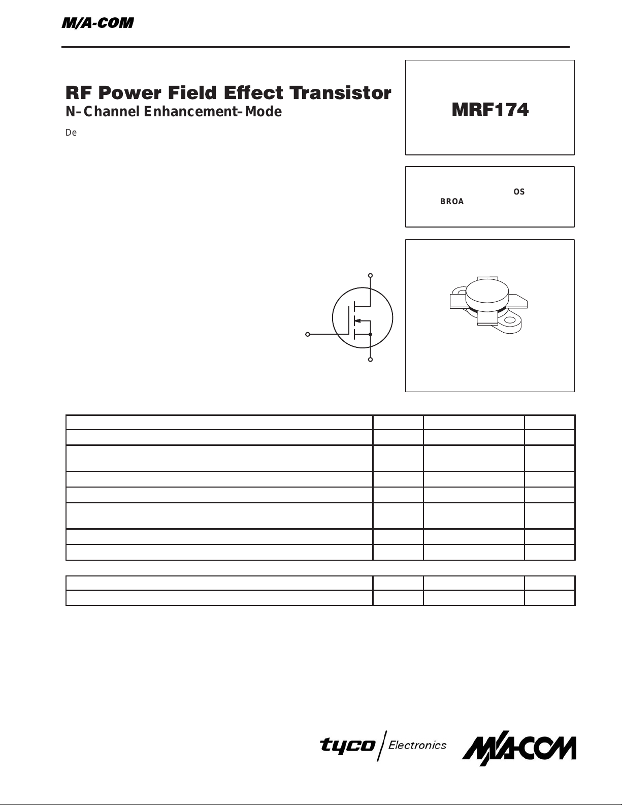
MRF174
125 W, to 200 MHz
N–CHANNEL MOS
BROADBAND RF POWER
FET
G
S
CASE 211–11, STYLE 2
MAXIMUM RATINGS
Rating Symbol Value Unit
Drain–Source Voltage V
Drain–Gate Voltage
(RGS = 1.0 MΩ)
Gate–Source Voltage V
Drain Current — Continuous I
Total Device Dissipation @ TC = 25°C
Derate above 25°C
Storage Temperature Range T
Operating Junction Temperature T
V
DSS
DGR
GS
D
P
D
stg
J
65 Vdc
65 Vdc
±40 Vdc
13 Adc
270
1.54
–65 to +150 °C
200 °C
Watts
W/°C
THERMAL CHARACTERISTICS
Characteristic Symbol Max Unit
Thermal Resistance, Junction to Case R
Handling and Packaging — MOS devices are susceptible to damage from electrostatic charge. Reasonable precautions in handling and
packaging MOS devices should be observed.
θJC
0.65 °C/W
REV 7
1
Page 2
ELECTRICAL CHARACTERISTICS (T
Characteristic Symbol Min Typ Max Unit
= 25°C unless otherwise noted.)
C
OFF CHARACTERISTICS
Drain–Source Breakdown Voltage (VGS = 0, ID = 50 mA) V
Zero Gate Voltage Drain Current (VDS = 28 V, VGS = 0) I
Gate–Source Leakage Current (VGS = 20 V, VDS = 0) I
ON CHARACTERISTICS
Gate Threshold Voltage (VDS = 10 V, ID = 100 mA) V
Forward Transconductance (VDS = 10 V, ID = 3.0 A) g
DYNAMIC CHARACTERISTICS
Input Capacitance (VDS = 28 V, VGS = 0, f = 1.0 MHz) C
Output Capacitance (VDS = 28 V, VGS = 0, f = 1.0 MHz) C
Reverse Transfer Capacitance (VDS = 28 V, VGS = 0, f = 1.0 MHz) C
FUNCTIONAL CHARACTERISTICS (Figure 1)
Noise Figure
(VDD = 28 Vdc, ID = 2.0 A, f = 150 MHz)
Common Source Power Gain
(VDD = 28 Vdc, P
Drain Efficiency
(VDD = 28 Vdc, P
Electrical Ruggedness
(VDD = 28 Vdc, P
VSWR 30:1 at all Phase Angles)
= 125 W, f = 150 MHz, IDQ = 100 mA)
out
= 125 W, f = 150 MHz, IDQ = 100 mA)
out
= 125 W, f = 150 MHz, IDQ = 100 mA,
out
(BR)DSS
DSS
GSS
GS(th)
fs
iss
oss
rss
NF — 3.0 — dB
G
ps
η 50 60 — %
ψ
65 — — Vdc
— — 10 mAdc
— — 1.0 µAdc
1.0 3.0 6.0 Vdc
1.75 2.5 — mhos
— 175 — pF
— 190 — pF
— 40 — pF
9.0 11.8 — dB
No Degradation in Output Power
ADJUST
RF INPUT
BIAS
R2
+
C9 C10
C3
C2
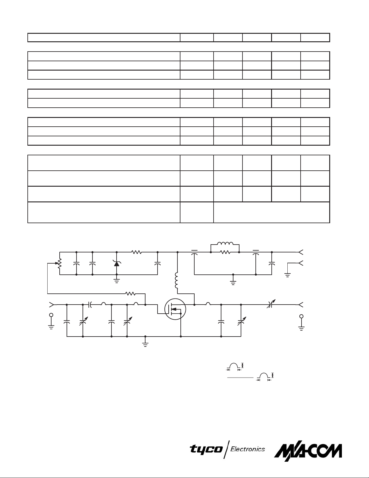
C1 — 15 pF Unelco
C2 — Arco 462, 5.0–80 pF
C3 — 100 pF Unelco
C4 — 25 pF Unelco
C6 — 40 pF Unelco
C7 — Arco 461, 2.7–30 pF
C5, C8 — Arco 463, 9.0–180 pF
C9, C11, C14 — 0.1 µF Erie Redcap
C10 — 50 µF, 50 V
C12, C13 — 680 pF Feedthru
D1 — 1N5925A Motorola Zener
D1R3
–
L1 L2
C4
R4
C5
L4
C12
R1
C11
RFC1
L3
DUTC1
L1 — #16 AWG, 1–1/4 Turns, 0.213 ″ ID
L2 — #16 AWG, Hairpin 0.25″
L3 — #14 AWG, Hairpin
L4 — 10 Turns #16 AWG Enameled Wire on R1
RFC1 — 18 Turns #16 AWG Enameled Wire, 0.3″ ID
R1 — 10 Ω, 2.0 W
R2 — 1.8 kΩ, 1/2 W
R3 — 10 kΩ, 10 Turn Bourns
R4 — 10 kΩ, 1/4 W
C6
C13
C7
0.062″
C8
C14
0.47″
0.2″
+
VDD = 28 V
–
RF OUTPUT
REV 7
2
Figure 1. 150 MHz Test Circuit
Page 3
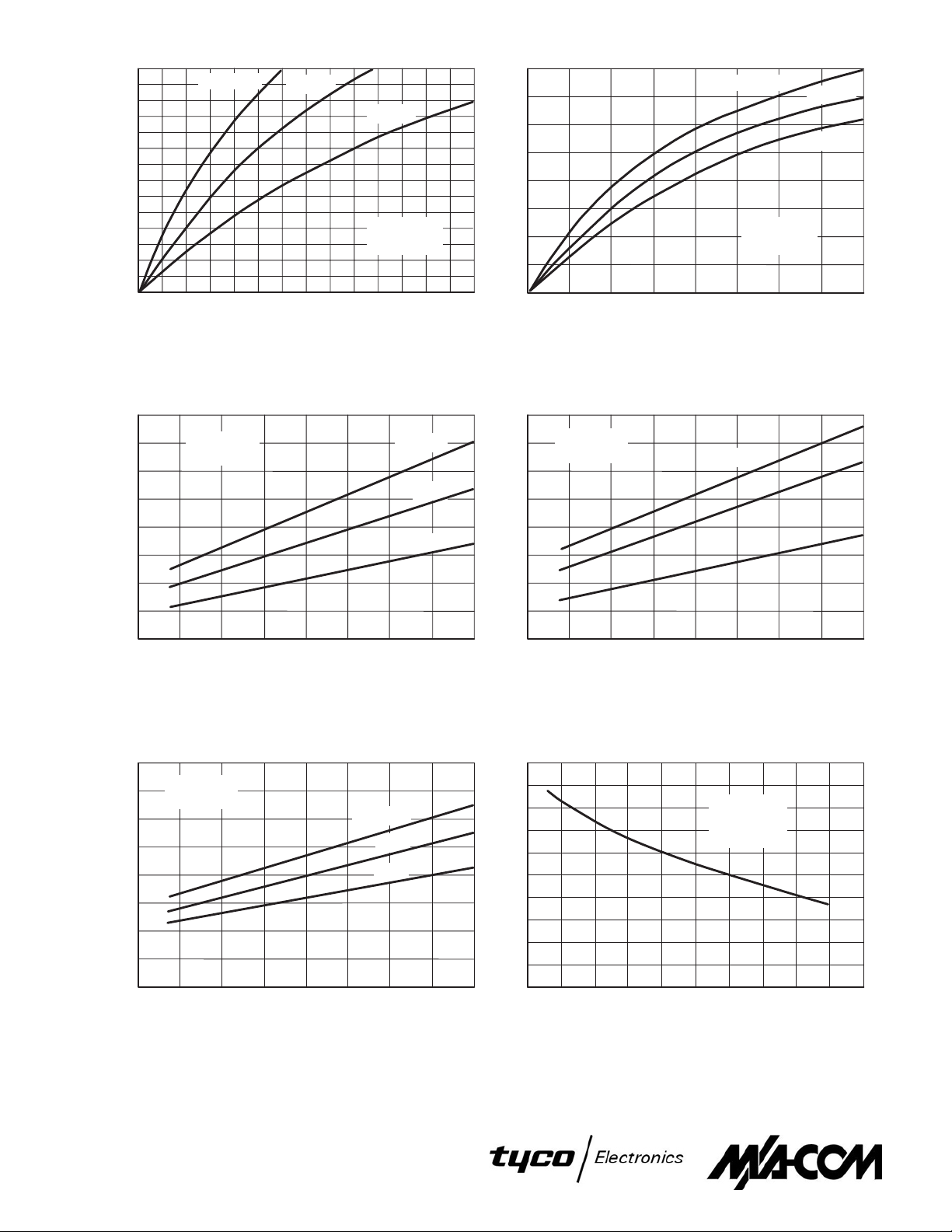
140
120
100
, OUTPUT POWER (WATTS)
out
P
, OUTPUT POWER (WATTS)
out
P
80
70
60
50
40
30
20
10
f = 100 MHz
VDD = 13.5 V
IDQ = 100 mA
150 MHz
200 MHz
f = 100 MHz
80
60
40
20
150 MHz
200 MHz
VDD = 28 V
IDQ = 100 mA
0
0
2
4 6 8 10 12 14
Pin, INPUT POWER (WA TTS)
0
0
46810121416
2
Pin, INPUT POWER (WA TTS)
Figure 2. Output Power versus Input Power Figure 3. Output Power versus Input Power
160
140
120
100
80
60
, OUTPUT POWER (WATTS)
40
out
P
20
0
12 2814 16 18 20 22 24 26
IDQ = 100 mA
f = 100 MHz
VDD, SUPPLY VOLTAGE (VOLTS)
Pin = 6 W
4 W
2 W
160
140
120
100
, OUTPUT POWER (WATTS)
out
P
IDQ = 100 mA
f = 150 MHz
80
60
40
20
0
12 2814 16 18 20 22 24 26
VDD, SUPPLY VOLTAGE (VOL TS)
Pin = 12 W
8 W
4 W
Figure 4. Output Power versus Supply Voltage Figure 5. Output Power versus Supply Voltage
160
140
120
100
, OUTPUT POWER (WATTS)
out
P
80
60
40
20
IDQ = 100 mA
f = 200 MHz
0
12 2814 16 18 20 22 24 26
VDD, SUPPLY VOLTAGE (VOL TS)
Figure 6. Output Power versus Supply Voltage Figure 7. Power Gain versus Frequency
REV 7
3
Pin = 16 W
12 W
8 W
22
20
18
16
14
12
10
, POWER GAIN (dB)
8
PS
G
6
4
2
20
40 60 80 100 120 140 160 180 200 220
P
out
VDD = 28 V
IDQ = 100 mA
f, FREQUENCY (MHz)
= 125 W
Page 4

160
140
120
100
, OUTPUT POWER (WATTS)
out
P
5
f = 150 MHz
Pin = CONSTANT
IDQ = 100 mA
VDD = 28 V
80
60
40
20
0
–12–14
VGS, GATE–SOURCE VOLTAGE (VOLTS)
TYPICAL DEVICE SHOWN, V
–8 0
–6 –4 –2 2 4 6–10
GS(th)
= 3 V
4
3
2
TYPICAL DEVICE SHOWN, V
, DRAIN CURRENT (AMPS)
D
I
1
0
123456
VDS = 10 V
= 3 V
GS(th)
VGS, GATE–SOURCE VOLTAGE (VOLTS)
Figure 8. Output Power versus Gate Voltage Figure 9. Drain Current versus Gate Voltage
(Transfer Characteristics)
1.2
1.1
1
0.9
, GATE-SOURCE VOLTAGE (NORMALIZED)
GS
V
0.8
–25
VDD = 28 V
ID = 4 A
0
25 50 75 100 125 150 175
TC, CASE TEMPERATURE (°C)
3 A
Figure 10. Gate–Source V oltage versus
Case T emperature
20
10
6
4
2
2 A
100 mA
TC = 25°C
1000
900
800
700
600
500
400
C, CAPACITANCE (pF)
300
200
100
0
04 812 20242816
VDS, DRAIN–SOURCE VOLTAGE (VOLTS)
Figure 11. Capacitance versus Drain Voltage
VGS = 0 V
f = 1 MHz
C
oss
C
iss
C
rss
REV 7
4
1
0.6
, DRAIN CURRENT (AMPS)
D
I
0.4
0.2
1
2 4 6 10 20 40 60 100
VDS, DRAIN–SOURCE VOLTAGE (VOLTS)
Figure 12. DC Safe Operating Area
Page 5

S
f
f
(MHz)
2.0 0.932 –133 74.0 112 0.011 23 0.835 –151
5.0 0.923 –160 31.6 98 0.011 12 0.886 –168
10 0.921 –170 16.0 93 0.011 10 0.896 –174
20 0.921 –175 8.00 88 0.011 12 0.899 –177
30 0.921 –177 5.32 86 0.011 16 0.900 –178
40 0.921 –177 3.98 83 0.012 21 0.901 –178
50 0.922 –178 3.17 81 0.012 26 0.902 –178
60 0.923 –178 2.63 79 0.012 30 0.903 –178
70 0.924 –178 2.24 77 0.013 34 0.904 –178
80 0.925 –178 1.95 75 0.013 39 0.906 –178
90 0.927 –178 1.72 73 0.014 43 0.907 –178
100 0.930 –178 1.50 71 0.016 45 0.910 –178
110 0.930 –178 1.31 70 0.018 46 0.912 –178
120 0.931 –178 1.19 68 0.019 47 0.914 –178
130 0.942 –178 1.10 67 0.019 49 0.919 –178
140 0.936 –178 1.01 66 0.021 50 0.921 –178
150 0.938 –178 0.936 65 0.021 53 0.922 –178
160 0.938 –178 0.879 64 0.022 53 0.923 –178
170 0.940 –178 0.830 63 0.023 54 0.923 –177
180 0.942 –178 0.780 61 0.024 56 0.924 –177
190 0.942 –178 0.737 60 0.026 59 0.928 –177
200 0.952 –178 0.705 59 0.027 58 0.929 –177
210 0.950 –178 0.668 57 0.029 61 0.934 –177
220 0.942 –178 0.626 56 0.030 61 0.933 –177
230 0.943 –178 0.592 56 0.032 62 0.939 –177
240 0.946 –177 0.566 55 0.033 64 0.941 –177
250 0.952 –177 0.545 54 0.035 64 0.943 –177
260 0.958 –177 0.523 53 0.036 65 0.946 –177
270 0.956 –177 0.500 52 0.038 67 0.943 –177
280 0.960 –177 0.481 52 0.039 68 0.946 –177
290 0.956 –178 0.460 51 0.042 68 0.944 –177
300 0.955 –178 0.443 50 0.043 68 0.947 –177
|S11| φ |S21| φ |S12| φ |S22| φ
11
S
21
S
12
S
22
T able 1. Common Source Scattering Parameters
VDS = 28 V, ID = 3.0 A
REV 7
5
Page 6

+j10
0
+j25
10
300
f = 30 MHz
+j50
+j100
25 50 100 150 250 500
+j150
+j250
+j500
–j500
180°
+150°
.05
.04 .03 .02 .01
+120°
+90°
+60°
300
250
200
150
100
50
f = 30 MHz
+30°
0°
–j10
–j25
–j50
Figure 13. S11, Input Reflection Coefficient
versus Frequency
VDS = 28 V, ID = 3.0 A
+90°
+120°
+150°
5 4 3 2 1
180°
f = 30 MHz
100
150
300
+60°
50
–j100
–j150
+30°
–j250
0°
–150°
–120°
–60°
–90°
–30°
Figure 14. S12, Reverse Transmission Coefficient
versus Frequency
VDS = 28 V, ID = 3.0 A
+j50
+j10
0
+j25
f = 30 MHz
300
25 50 100 150 250 500
+j100
+j150
+j250
+j500
–j500
–150°
–120°
–60°
–90°
–30°
Figure 15. S21, Forward Transmission Coefficient
versus Frequency
VDS = 28 V, ID = 3.0 A
REV 7
6
–j10
–j150
–j25
–j50
–j100
Figure 16. S22, Output Reflection Coefficient
versus Frequency
VDS = 28 V, ID = 3.0 A
–j250
Page 7

150
f = 200 MHz
100
100
Z
in
30
30
ZOL* = Conjugate of the optimum load impedance
ZOL* = into which the device output operates at a
ZOL* = given output power, voltage and frequency.
150
ZOL*
Zo = 10 Ω
f = 200 MHz
MHz
30
100
150
200
P
out
f
Figure 17. Series Equivalent Input/Output Impedance, Zin, ZOL*
= 125 W, VDD = 28 V
IDQ = 100 mA
Z
in
Ohms
2.90 – j3.95
1.25 – j2.90
1.18 – j1.40
1.30 – j0.90
ZOL*
Ohms
2.95 – j3.90
1.85 – j1.05
1.72 – j0.05
1.70 + j0.25
REV 7
7
Page 8

DESIGN CONSIDERATIONS
The MRF174 is a RF power N–Channel enhancement
mode field–effect transistor (FET) designed especially for
UHF power amplifier and oscillator applications. M/A-COM RF
MOSFETs feature a vertical structure with a planar design,
thus avoiding the processing difficulties associated with V–
groove vertical power FETs.
M/A-COM Application Note AN211A, FETs in Theory and
Practice, is suggested reading for those not familiar with the
construction and characteristics of FETs.
The major advantages of RF power FETs include high
gain, low noise, simple bias systems, relative immunity from
thermal runaway, and the ability to withstand severely mismatched loads without suffering damage. Power output can
be varied over a wide range with a low power dc control signal, thus facilitating manual gain control, ALC and modulation.
DC BIAS
The MRF174 is an enhancement mode FET and, therefore, does not conduct when drain voltage is applied. Drain
current flows when a positive voltage is applied to the gate.
See Figure 9 for a typical plot of drain current versus gate
voltage. RF power FETs require forward bias for optimum
performance. The value of quiescent drain current (IDQ) is
not critical for many applications. The MRF174 was charac-
terized at IDQ = 100 mA, which is the suggested minimum
value of IDQ. For special applications such as linear amplification, IDQ may have to be selected to optimize the critical
parameters.
The gate is a dc open circuit and draws no current. Therefore, the gate bias circuit may generally be just a simple resistive divider network. Some special applications may
require a more elaborate bias system.
GAIN CONTROL
Power output of the MRF174 may be controlled from its
rated value down to zero (negative gain) by varying the dc
gate voltage. This feature facilitates the design of manual
gain control, AGC/ALC and modulation systems. (See
Figure 8.)
AMPLIFIER DESIGN
Impedance matching networks similar to those used with
bipolar UHF transistors are suitable for MRF174. See
M/A-COM Application Note AN721, Impedance Matching Networks Applied to RF Power Transistors. The higher input
impedance of RF MOSFETs helps ease the task of broadband network design. Both small signal scattering parameters and large signal impedances are provided. While the
s–parameters will not produce an exact design solution for
high power operation, they do yield a good first approximation. This is an additional advantage of RF MOS power FET s.
REV 7
8
Page 9

P ACKAGE DIMENSIONS
A
U
M
Q
1
4
32
M
R
B
D
K
J
H
C
E
SEATING
PLANE
NOTES:
1. DIMENSIONING AND TOLERANCING PER ANSI
Y14.5M, 1982.
2. CONTROLLING DIMENSION: INCH.
DIM MIN MAX MIN MAX
A 0.960 0.990 24.39 25.14
B 0.465 0.510 11.82 12.95
C 0.229 0.275 5.82 6.98
D 0.216 0.235 5.49 5.96
E 0.084 0.110 2.14 2.79
H 0.144 0.178 3.66 4.52
J 0.003 0.007 0.08 0.17
K 0.435 ––– 11.05 –––
M 45 NOM 45 NOM
__
Q 0.115 0.130 2.93 3.30
R 0.246 0.255 6.25 6.47
U 0.720 0.730 18.29 18.54
STYLE 2:
PIN 1. SOURCE
2. GATE
3. SOURCE
4. DRAIN
MILLIMETERSINCHES
CASE 211–11
ISSUE N
Specifications subject to change without notice.
n
North America: Tel. (800) 366-2266, Fax (800) 618-8883
n Asia/Pacific: Tel.+81-44-844-8296, Fax +81-44-844-8298
n
Europe: Tel. +44 (1344) 869 595, Fax+44 (1344) 300 020
Visit www.macom.com for additional data sheets and product information.
REV 7
9
 Loading...