

Page 1
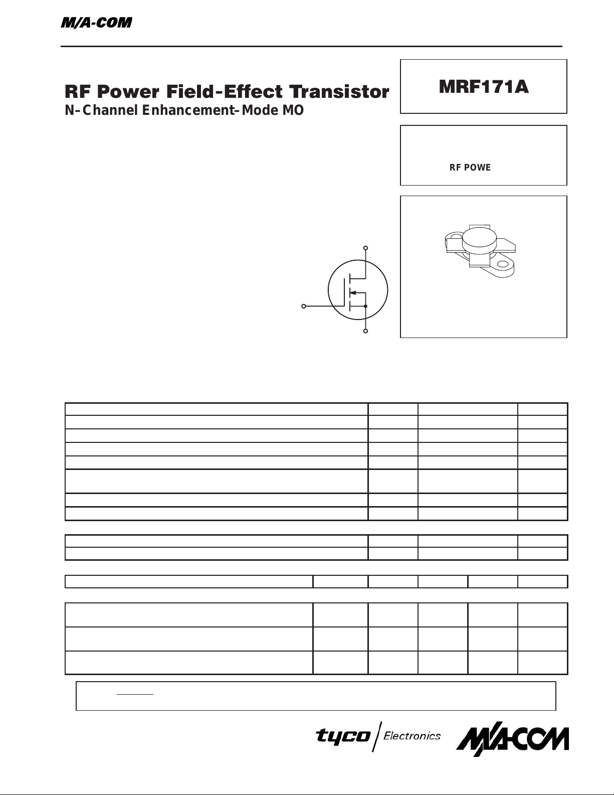
SEMICONDUCTOR TECHNICAL DATA
The RF MOSFET Line
RF Power Field-Effect Transistor
N–Channel Enhancement–Mode MOSFET
Designed primarily for wideband large–signal output and driver stages from
30–200 MHz.
• Guaranteed Performance at 150 MHz, 28 Vdc
Output Power = 45 Watts
Power Gain = 17 dB (Min)
Efficiency = 60% (Min)
• Excellent Thermal Stability , Ideally Suited for Class A Operation
• Facilitates Manual Gain Control, ALC and Modulation Techniques
• 100% Tested for Load Mismatch At All Phase Angles with 30:1 VSWR
• Low Crss – 8 pF @ VDS = 28 V
• Gold Top Metal
Typical Data For Power Amplifier Applications in Industrial,
Commercial and Amateur Radio Equipment
• Typical Performance at 30 MHz, 28 Vdc
Output Power = 30 Watts (PEP)
Power Gain = 20 dB (Typ)
Efficiency = 50% (Typ)
IMD(d3) (30 Watts PEP) –32 dB (Typ)
G
D
S
Order this document
by MRF171A/D
MRF171A
45 W, 150 MHz
MOSFET BROADBAND
RF POWER FET
CASE 211–07, STYLE 2
MAXIMUM RATINGS
Rating Symbol Value Unit
Drain–Gate Voltage V
Drain–Gate Voltage (RGS = 1.0 MΩ) V
Gate–Source Voltage V
Drain Current — Continuous I
Total Device Dissipation @ TC = 25°C
Derate above 25°C
Storage Temperature Range T
Operating Junction Temperature T
THERMAL CHARACTERISTICS
Characteristic Symbol Max Unit
Thermal Resistance, Junction to Case R
ELECTRICAL CHARACTERISTICS (T
Characteristic
= 25°C unless otherwise noted)
C
Symbol Min Typ Max Unit
OFF CHARACTERISTICS
Drain–Source Breakdown Voltage
(ID = 50 mA, VGS = 0)
Zero Gate Voltage Drain Current
(VGS = 0, VDS = 28 V)
Gate–Source Leakage Current
(VGS = 20 V, VDS = 0)
V
(BR)DSS
I
DSS
I
GSS
DSS
DGR
GS
D
P
D
stg
J
θJC
65 80 — Vdc
— — 1.0 mAdc
— — 1.0 µAdc
65 Vdc
65 Vdc
±20 Adc
4.5 Adc
115
0.66
–65 to +150 °C
200 °C
1.52 °C/W
Watts
W/°C
NOTE – CAUTION – MOS devices are susceptible to damage from electrostatic charge. Reasonable precautions in handling and
packaging MOS devices should be observed.
REV 2
1
Page 2
ELECTRICAL CHARACTERISTICS – continued (T
Characteristic
ON CHARACTERISTICS
Gate Threshold Voltage
(VDS = 10 V, ID = 50 mA)
Drain–Source On–Voltage
(VGS = 10 V, ID = 3 A)
Forward Transconductance
(VDS = 10 V, ID = 2 A)
DYNAMIC CHARACTERISTICS
Input Capacitance
(VDS = 28 V, VGS = 0, f = 1.0 MHz)
Output Capacitance
(VDS = 28 V, VGS = 0, f = 1.0 MHz)
Reverse Transfer Capacitance
(VDS = 28 V, VGS = 0, f = 1.0 MHz)
FUNCTIONAL CHARACTERISTICS
Common Source Power Gain
(VDD = 28 V, P
Drain Efficiency
(VDD = 28 V, Pout = 45 W, f = 150 MHz, IDQ = 25 mA)
Electrical Ruggedness
(VDD = 28 V, P
VSWR 30:1 at All Phase Angles)
= 45 W, f = 150 MHz, IDQ = 25 mA)
out
= 45 W, f = 150 MHz, IDQ = 25 mA,
out
TYPICAL FUNCTIONAL TESTS (SSB)
Common Source Power Gain
(VDD = 28 V, P
f = 30; 30.001 MHz)
Drain Efficiency
(VDD = 28 V, P
f = 30; 30.001 MHz)
Intermodulation Distortion
(VDD = 28 V, P
f = 30; 30.001 MHz)
= 30 W (PEP), IDQ = 100 mA,
out
= 30 W (PEP), IDQ = 100 mA,
out
= 30 W (PEP), IDQ = 100 mA,
out
= 25°C unless otherwise noted)
C
Symbol Min Typ Max Unit
V
GS(th)
V
DS(on)
g
fs
C
iss
C
oss
C
rss
G
ps
η 60 70 — %
G
ps
η — 50 — %
IMD(d3)
1.5 2.5 4.5 Vdc
— 1.0 — V
1.4 1.8 — mhos
— 60 — pF
— 70 — pF
— 8 — pF
17 19.5 — dB
No Degradation in Output Power
— 20 — dB
— –32 — dB
REV 2
2
Page 3
RF
INPUT
BIAS
+ +
Z1 Z2 Z3 Z4
C3
C2
C1
R2
R3
L1
C4
C5
C6 C13
L2
R1
RFC2
Z5
DUT
RFC1
C14
C11
L3
C7
Z6 L4 Z7
C8
C12
C9
VDD 28 Vdc
+
V
DC
–
RF
OUTPUT
C10
C1, C10 1000 pF, Chip Capacitor
C2, C5, C8 2–20 pF, Trimmer Capacitors, Johanson
C3 43 pF, 100 mil Chip Capacitor, ATC
C4 120 pF, 100 mil Chip Capacitor, ATC
C6, C14 0.1 µF, Capacitors
C7 50 pF, 100 mil Chip Capacitor, ATC
C9 12 pF, 100 mil Chip Capacitor, ATC
C11, C12 680 pF, Feedthru Capacitors
C13 50 µF, 50 V, Electrolytic Capacitor
L1 2 Turns, 0.297″ ID, 18 AWG
L2 1–1/2 Turns, 0.265″ ID, 18 AWG
L3 1–1/4 Turns, 0.234″ ID, 18 AWG
L4 1–1/2 Turns, 0.250″ ID, 18 AWG
R1 68 Ω, 1/2 W Chip Resistor
Figure 1. MRF171A 150 MHz T est Circuit
R2 1 kΩ, 1/2 W Chip Resistor
R3 10 kΩ, 1/2 W Chip Resistor
Z1 0.160″ x 0.400″ Microstrip
Z2 0.160″ x 0.600″ Microstrip
Z3 0.160″ x 0.600″ Microstrip
Z4 0.160″ x 0.900″ Microstrip
Z5 0.160″ x 0.800″ Microstrip
Z6 0.160″ x 0.800″ Microstrip
Z7 0.160″ x 0.400″ Microstrip
RFC1 Ferroxcube VK200–19/4B
RFC2 10 Turns, 0.250″ ID, 20 AWG, Enamel
Board 0.062″, G10 1 oz. Copper Clad
Both Sides, εr = 2.56
REV 2
3
Page 4

28 V
L2
C8
C9
L1
V
GG
+
C10
+
+
C11
C1 C2
C3
RF
INPUT
T1
C1, C3, C5, C6 0.1 µF, Chip Capacitors
C2, C4 1000 pF, Chip Capacitors
C7 68 pF, Dipped Mica
C8 0.1 µF, Ceramic Cap or Equivalent
C9, C10 680 pF, Feedthru Capacitors
C11 250 µF, 50 V, Electrolytic Capacitor
R3
Figure 2. MRF171A 30 MHz Test Circuit
R1
R2
C4 C5
RF
OUTPUT
C7
DUT
C6
R4
L1, L2 VK200 20/4B Ferrite Choke
R1, R2 200 Ω, 1/2 W Carbon
R3 3 Ω, 1/2 W Carbon
R4 270 Ω, 2 W Carbon
T1 4:1 Impedance Broadband Transformer
T2 1:4 Impedance Broadband Transformer
T2
REV 2
4
Page 5

TYPICAL CHARACTERISTICS
60
50
40
30
20
, OUTPUT POWER (WATTS) PEP
10
out
P
0
0
0.2 0.6 1.0
0.4
Pin, INPUT POWER (WA TTS) PEP
VDD = 28 V
IDQ = 100 mA
f = 30 MHz
TONE SEPARATION = 1 kHz
0.50.3 0.80.1 0.7 0.9
Figure 3. Output Power versus Input Power
, OUTPUT POWER (WATTS)
out
P
18
16
14
12
10
8
6
4
2
0
f = 100 MHz
0.1 0.2 0.3 0.6 0.7 0.80.5
0
Pin, INPUT POWER (WA TTS)
150 MHz
0.4
200 MHz
VDD = 13.5 V
IDQ = 25 mA
0.9
, OUTPUT POWER (WATTS)
out
P
70
60
50
40
30
20
10
0
f = 100 MHz
150 MHz
200 MHz
0.80.4 1.2 2.00 1.00.6 1.60.2 1.4 1.8
Pin, INPUT POWER (WA TTS)
Figure 4. Output Power versus Input Power
70
60
50
40
30
, OUTPUT POWER (WATTS)
20
out
P
10
0
14 18
16
VDD, DRAIN SUPPLY VOLTAGE (VOL TS)
20 2212
VDD = 28 V
IDQ = 25 mA
Pin = 1.0 W
0.5 W
0.1 W
IDQ = 25 mA
f = 100 MHz
24 26 28
Figure 5. Output Power versus Input Power
70
, OUTPUT POWER (WATTS)
out
P
60
50
40
30
20
10
0
14 16 20 22 24 28
12
18
VDD, SUPPLY VOLTAGE (VOLTS)
Pin = 2.0 W
1.0 W
0.3 W
IDQ = 25 mA
f = 150 MHz
Figure 7. Output Power versus Supply Voltage
REV 2
5
Figure 6. Output Power versus Supply Voltage
80
70
60
50
40
30
, OUTPUT POWER (WATTS)
20
out
P
10
26
0
12 261814 16 20 22 24 28
VDD, SUPPLY VOLTAGE (VOLTS)
Pin = 4.0 W
3.0 W
2.0 W
IDQ = 25 mA
f = 200 MHz
Figure 8. Output Power versus Supply Voltage
Page 6

TYPICAL CHARACTERISTICS
3.0
VDS = 10 V
2.5
TYPICAL DEVICE SHOWN,
V
= 2.5 V
GS(th)
2.0
1.5
1.0
, DRAIN CURRENT (AMPS)
D
I
0.5
0.0
1.0 3.0 5.0
VGS, GATE–SOURCE VOLTAGE (VOLTS)
2.0
2.51.5 4.50.5 3.5 4.0
Figure 9. Drain Current versus Gate Voltage
(Transfer Characteristics)
1000
100
45
Pin = CONSTANT
40
VDD = 28 V
35
IDQ = 25 mA
f = 150 MHz
30
TYPICAL DEVICE SHOWN,
25
V
= 2.5 V
GS(th)
20
15
, OUTPUT POWER (WATTS)
10
out
P
5
0
–1.0 2.50
0
VGS, GATE–SOURCE VOLTAGE (VOLTS)
1.0 2.0
0.5–0.5 1.5
Figure 10. Output Power versus Gate Voltage
C
oss
C
iss
C
rss
VGS = 0 V
f = 1 MHz
20
C, CAPACITANCE (pF)
10
1
0
51015 25
VDS, DRAIN–SOURCE VOLTAGE (VOLTS)
Figure 11. Capacitance versus Drain–Source Voltage
30
REV 2
6
Page 7

200
150
200
Zo = 10 Ω
f = 30 MHz
ZOL*
100
f = 30 MHz
Z
in
150
VDD = 28 V, IDQ = 25 mA, P
f
MHz
30
100
150
200
(1) 68 Ω shunt resistor gate–to–ground.
(2) ZOL= Conjugate of the optimum load impedance
Zin(1)
Ω
12.8 – j3.6
3.1 – j11.6
2.0 – j6.5
2.2 – j6.0
into which the device operates at a given
output power, voltage and frequency.
100
= 45 W
out
ZOL(2)
11.5 – j0.99
4.9 – j4.9
4.2 – j4.9
3.0 – j2.9
Ω
Figure 12. Large–Signal Series Equivalent Input/Output Impedance
REV 2
7
Page 8

Figure 13. MRF171A Circuit Board Photo Master
(Scale 1:1)
REV 2
8
Page 9

f
MHz
ÁÁÁÁ
ÁÁÁÁ
ÁÁÁÁ
ÁÁÁÁ
ÁÁÁÁ
ÁÁÁÁ
ÁÁÁÁ
ÁÁÁÁ
ÁÁÁÁ
ÁÁÁÁ
ÁÁÁÁ
ÁÁÁÁ
ÁÁÁÁ
ÁÁÁÁ
ÁÁÁÁ
ÁÁÁÁ
ÁÁÁÁ
ÁÁÁÁ
ÁÁÁÁ
ÁÁÁÁ
ÁÁÁÁ
ÁÁÁÁ
ÁÁÁÁ
ÁÁÁÁ
ÁÁÁÁ
ÁÁÁÁ
ÁÁÁÁ
ÁÁÁÁ
ÁÁÁÁ
ÁÁÁÁ
ÁÁÁÁ
ÁÁÁÁ
ÁÁÁÁ
ÁÁÁÁ
ÁÁÁÁ
ÁÁÁÁ
ÁÁÁÁ
ÁÁÁÁ
ÁÁÁÁ
ÁÁÁÁ
ÁÁÁÁ
ÁÁÁÁ
30
40
50
60
70
80
90
100
110
120
130
140
150
160
170
180
190
200
210
220
230
240
250
260
270
280
290
300
310
320
330
340
350
360
370
380
390
400
410
420
430
440
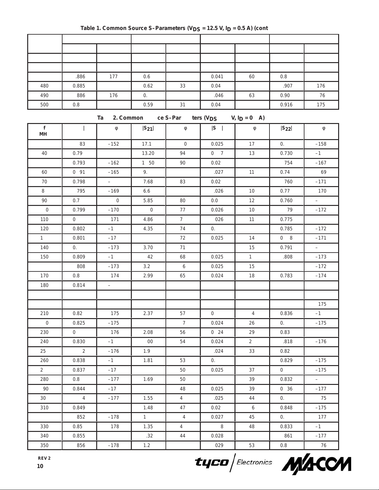
T able 1. Common Source S–Parameters (VDS = 12.5 V, ID = 0.5 A)
S
11
|S11| φ |S21| φ |S12| φ |S22| φ
0.801
0.809
0.810
0.808
0.814
0.811
0.811
0.814
0.812
0.816
0.816
0.817
0.821
0.820
0.821
0.824
0.825
0.830
0.831
0.831
0.836
0.836
0.839
0.844
0.842
0.845
0.849
0.849
0.855
0.856
0.856
0.858
0.860
0.862
0.866
0.867
0.869
0.870
0.872
0.876
0.877
0.879
–162
–166
–169
–170
–172
–173
–174
–174
–175
–175
–176
–176
–176
–176
–177
–177
–177
–177
–177
–178
–178
–178
–178
–178
–178
–179
–179
–179
–179
–179
–180
–180
180
180
180
179
179
179
179
178
178
178
11.90
9.12
7.29
6.22
5.30
4.56
4.04
3.66
3.37
3.00
2.75
2.57
2.37
2.27
2.08
1.93
1.89
1.74
1.67
1.62
1.48
1.43
1.37
1.30
1.28
1.21
1.14
1.12
1.06
1.03
0.96
0.96
0.93
0.91
0.86
0.84
0.82
0.78
0.77
0.73
0.69
0.68
S
21
96
91
88
85
82
81
80
77
75
74
73
72
69
67
66
65
64
62
60
59
57
56
57
54
52
52
50
50
49
46
45
46
44
44
43
41
42
40
39
37
38
39
0.026
0.028
0.027
0.028
0.028
0.027
0.027
0.027
0.027
0.027
0.027
0.027
0.027
0.027
0.026
0.027
0.027
0.027
0.027
0.026
0.027
0.027
0.028
0.028
0.028
0.027
0.027
0.029
0.029
0.030
0.031
0.030
0.031
0.033
0.034
0.036
0.035
0.035
0.037
0.039
0.040
0.041
S
12
13
11
11
9
9
10
13
12
11
13
14
17
17
17
19
19
21
23
25
28
27
26
30
34
36
37
36
39
42
43
47
47
49
48
50
52
54
57
55
54
56
58
0.811
0.812
0.831
0.824
0.831
0.837
0.829
0.846
0.842
0.850
0.849
0.851
0.863
0.853
0.838
0.861
0.873
0.873
0.874
0.870
0.909
0.865
0.873
0.882
0.887
0.881
0.869
0.852
0.891
0.889
0.868
0.888
0.875
0.901
0.913
0.897
0.893
0.880
0.923
0.915
0.903
0.921
S
22
–166
–171
–172
–174
–176
–175
–174
–176
–177
–176
–175
–176
–177
–177
–177
–177
–177
–178
–177
–178
–179
–180
–178
–179
–180
–180
179
–180
–179
180
180
179
–180
179
178
178
178
180
178
176
177
178
REV 2
9
Page 10
f
ÁÁÁÁ
ÁÁÁÁ
ÁÁÁÁ
ÁÁÁÁ
ÁÁÁÁ
ÁÁÁÁ
ÁÁÁÁ
ÁÁÁÁ
ÁÁÁÁ
ÁÁÁÁ
ÁÁÁÁ
ÁÁÁÁ
ÁÁÁÁ
ÁÁÁÁ
ÁÁÁÁ
ÁÁÁÁ
ÁÁÁÁ
ÁÁÁÁ
ÁÁÁÁ
ÁÁÁÁ
ÁÁÁÁ
ÁÁÁÁ
ÁÁÁÁ
ÁÁÁÁ
ÁÁÁÁ
ÁÁÁÁ
ÁÁÁÁ
ÁÁÁÁ
ÁÁÁÁ
ÁÁÁÁ
ÁÁÁÁ
ÁÁÁÁ
ÁÁÁÁ
ÁÁÁÁ
ÁÁÁÁ
ÁÁÁÁ
ÁÁÁÁ
ÁÁÁÁ
ÁÁÁÁ
f
MHz
MHz
450
460
470
480
490
500
f
MHz
30
40
50
60
70
80
90
100
110
120
130
140
150
160
170
180
190
200
210
220
230
240
250
260
270
280
290
300
310
320
330
340
350
T able 1. Common Source S–Parameters (VDS = 12.5 V, ID = 0.5 A) (continued)
S
22
178
175
176
176
176
175
0.882
0.884
0.886
0.885
0.886
0.887
S
12
61
59
60
61
63
65
0.926
0.937
0.896
0.907
0.907
0.916
0.68
0.65
0.62
0.62
0.61
0.59
S
21
36
36
35
33
32
31
0.040
0.041
0.041
0.044
0.046
0.047
S
11
177
177
177
176
176
176
T able 2. Common Source S–Parameters (VDS = 28 V, ID = 0.5 A)
|S11| φ |S21| φ |S12| φ |S22| φ
0.783
0.793
0.793
0.791
0.798
0.795
0.795
0.799
0.798
0.802
0.801
0.803
0.809
0.808
0.809
0.814
0.815
0.822
0.824
0.825
0.831
0.830
0.832
0.838
0.837
0.840
0.844
0.844
0.849
0.852
0.852
0.855
0.856
–152
–158
–162
–165
–167
–169
–170
–170
–171
–172
–172
–173
–173
–173
–174
–174
–175
–175
–175
–175
–176
–176
–176
–176
–176
–177
–177
–177
–178
–178
–178
–178
–178
17.10
13.20
10.50
9.00
7.68
6.63
5.85
5.30
4.86
4.35
3.97
3.70
3.42
3.27
2.99
2.77
2.71
2.49
2.37
2.23
2.08
2.00
1.92
1.81
1.79
1.69
1.60
1.55
1.48
1.43
1.35
1.32
1.29
100
94
90
87
83
82
80
77
75
74
72
71
68
66
65
63
62
60
57
57
56
54
55
53
50
50
48
48
47
44
43
44
41
0.025
0.027
0.027
0.027
0.026
0.026
0.026
0.026
0.026
0.025
0.025
0.025
0.025
0.025
0.024
0.025
0.024
0.024
0.024
0.024
0.024
0.024
0.024
0.024
0.025
0.025
0.025
0.025
0.026
0.027
0.028
0.028
0.029
17
13
12
11
10
10
12
10
11
13
14
15
14
15
18
19
21
22
24
26
29
29
33
35
37
39
39
44
46
45
48
49
53
0.730
0.730
0.754
0.746
0.760
0.770
0.760
0.779
0.775
0.785
0.788
0.791
0.808
0.796
0.783
0.809
0.820
0.826
0.836
0.807
0.839
0.818
0.828
0.829
0.834
0.832
0.836
0.814
0.848
0.855
0.833
0.861
0.842
–158
–164
–167
–169
–171
–170
–170
–172
–174
–172
–171
–172
–173
–172
–174
–173
–174
–175
–175
–175
–175
–176
–174
–175
–175
–176
–177
–175
–175
–177
–177
–177
–176
φ|S22|φ|S12|φ|S21|φ|S11|
REV 2
10
Page 11

f
ÁÁÁÁ
ÁÁÁÁ
ÁÁÁÁ
ÁÁÁÁ
ÁÁÁÁ
ÁÁÁÁ
ÁÁÁÁ
ÁÁÁÁ
ÁÁÁÁ
ÁÁÁÁ
ÁÁÁÁ
ÁÁÁÁ
ÁÁÁÁ
ÁÁÁÁ
ÁÁÁÁ
MHz
360
370
380
390
400
410
420
430
440
450
460
470
480
490
500
T able 2. Common Source S–Parameters (VDS = 28 V, ID = 0.5 A) (continued)
0.859
0.863
0.864
0.867
0.869
0.872
0.876
0.877
0.879
0.882
0.884
0.885
0.885
0.886
0.887
–179
–179
–179
–179
–180
–180
180
179
179
179
178
178
178
177
177
1.25
1.18
1.15
1.12
1.07
1.05
1.00
0.95
0.93
0.91
0.88
0.84
0.83
0.81
0.80
42
39
38
39
37
35
34
35
34
32
32
32
30
29
28
0.030
0.030
0.031
0.032
0.032
0.035
0.036
0.037
0.038
0.039
0.041
0.040
0.042
0.044
0.045
54
55
55
57
60
60
60
62
64
65
64
66
66
68
68
0.872
0.886
0.864
0.862
0.853
0.898
0.889
0.884
0.902
0.901
0.922
0.877
0.892
0.891
0.900
φ|S22|φ|S12|φ|S21|φ|S11|
–178
–178
–178
–179
–177
–179
180
–179
–179
–180
179
179
179
179
178
REV 2
11
Page 12

P ACKAGE DIMENSIONS
A
U
M
Q
1
4
32
S
K
M
B
R
D
J
H
C
E
SEATING
PLANE
NOTES:
1. DIMENSIONING AND TOLERANCING PER ANSI
Y14.5M, 1982.
2. CONTROLLING DIMENSION: INCH.
DIM MIN MAX MIN MAX
A 0.960 0.990 24.39 25.14
B 0.370 0.390 9.40 9.90
C 0.229 0.281 5.82 7.13
D 0.215 0.235 5.47 5.96
E 0.085 0.105 2.16 2.66
H 0.150 0.108 3.81 4.57
J 0.004 0.006 0.11 0.15
K 0.395 0.405 10.04 10.28
M 40 50 40 50
____
Q 0.113 0.130 2.88 3.30
R 0.245 0.255 6.23 6.47
S 0.790 0.810 20.07 20.57
U 0.720 0.730 18.29 18.54
STYLE 2:
PIN 1. SOURCE
2. GATE
3. SOURCE
4. DRAIN
MILLIMETERSINCHES
CASE 211–07
ISSUE N
Specifications subject to change without notice.
n
North America: Tel. (800) 366-2266, Fax (800) 618-8883
n Asia/Pacific: Tel.+81-44-844-8296, Fax +81-44-844-8298
n
Europe: Tel. +44 (1344) 869 595, Fax+44 (1344) 300 020
Visit www.macom.com for additional data sheets and product information.
REV 2
12
 Loading...