

Page 1
SEMICONDUCTOR TECHNICAL DATA
The RF MOSFET Line
Power Field Effect Transistor
N–Channel Enhancement–Mode MOSFET
Designed primarily for wideband large–signal output and driver stages to
30 – 500 MHz.
• Push–Pull Configuration Reduces Even Numbered Harmonics
• Guaranteed Performance at 500 MHz, 28 Vdc
Output Power = 40 Watts
Gain = 14 dB
Efficiency = 50%
• Typical Performance at 175 MHz, 28 Vdc
Output Power = 40 Watts
Gain = 17 dB
Efficiency = 60%
• Excellent Thermal Stability , Ideally Suited for Class A Operation
• Facilitates Manual Gain Control, ALC and Modulation Techniques
• 100% Tested for Load Mismatch at All Phase Angles with 30:1 VSWR
• Low C
— 4.0 pF @ VDS = 28 Volts
rss
Order this document
by MRF166W/D
MRF166W
40 W, 500 MHz
TMOS BROADBAND
RF POWER FET
MAXIMUM RATINGS
Drain–Gate Voltage V
Drain–Gate Voltage (RGS = 1.0 MΩ) V
Gate–Source Voltage V
Drain Current — Continuous I
Total Device Dissipation @ TC = 25°C
Derate above 25°C
Storage Temperature Range T
Operating Junction Temperature T
(TJ = 25°C unless otherwise noted)
Rating
THERMAL CHARACTERISTICS
Thermal Resistance — Junction to Case R
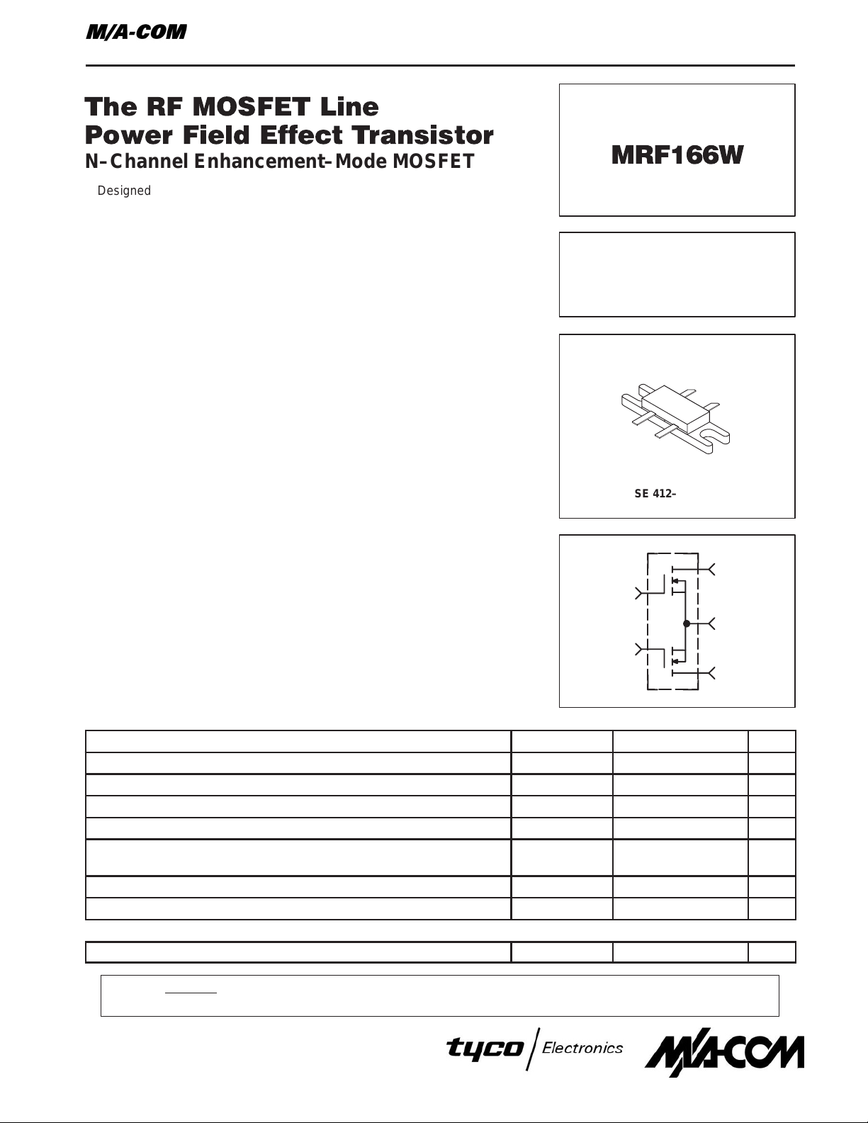
CASE 412–01, Style 1
1
3
5
4
Symbol Value Unit
DSS
DGR
GS
D
P
D
stg
J
θJC
–65 to +150 °C
FLANGE
2
65 Vdc
65 Vdc
± 20 Adc
8.0 ADC
175
1.0
200 °C
1.0 °C/W
Watts
°C/W
NOTE — CAUTION — MOS devices are susceptible to damage from electrostatic charge. Reasonable precautions in handling and
packaging MOS devices should be observed.
REV 3
1
Page 2
ELECTRICAL CHARACTERISTICS (T
Characteristic Symbol Min Typ Max Unit
= 25°C unless otherwise noted)
C
OFF CHARACTERISTICS (1)
Drain–Source Breakdown Voltage
(VGS = 0 Vdc, ID = 5.0 mA)
Zero Gate Voltage Drain Current
(VDS = 28 Vdc, VGS = 0 Vdc)
Gate–Source Leakage Current
(VGS = 20 Vdc, VDS = 0 Vdc)
ON CHARACTERISTICS (1)
Gate Threshold Voltage
(VDS= 10 Vdc, ID = 25 mA)
Forward Transconductance
(VDS= 10 Vdc, ID = 1.5 A)
DYNAMIC CHARACTERISTICS (1)
Input Capacitance
(VDS = 28 Vdc, VGS = 0 Vdc, f = 1.0 MHz)
Output Capacitance
(VDS = 28 Vdc, VGS = 0 Vdc, f = 1.0 MHz)
Reverse Transfer Capacitance
(VDS = 28 Vdc, VGS = 0 Vdc, f = 1.0 MHz)
FUNCTIONAL CHARACTERISTICS (2)
Common Source Power Gain
(VDD = 28 Vdc, P
Drain Efficiency
(VDD = 28 Vdc, P
Electrical Ruggedness
(VDD = 28 Vdc, P
Load VSWR = 30:1, All phase angles at frequency of test
Series Equivalent Input Impedance
(VDD = 28 Vdc, P
Series Equivalent Output Impedance
(VDD = 28 Vdc, P
(1) Each transistor chip measured separately.
(2) Both transistor chips operating in a push–pull amplifier.
= 40 W, f = 500 MHz, IDQ = 100 mA)
out
= 40 W, f = 500 MHz, IDQ = 100 mA)
out
= 40 W, f = 500 MHz, IDQ = 100 mA)
out
= 40 W, f = 500 MHz, IDQ = 100 mA)
out
= 40 W, f = 500 MHz, IDQ = 100 mA)
out
V
(BR)DSS
I
DSS
I
GSS
V
GS(th)
g
fs
C
iss
C
oss
C
rss
G
ps
η
Ψ
Z
in
Z
out
65 — —
Vdc
mA
— — 0.5
µA
— — 1.0
Vdc
1.5 3.0 4.5
mS
0.9 1.1 —
pF
— 28 —
pF
— 30 —
pF
— 4.0 —
dB
14 16 —
%
50 55 —
No Degradation in Output Power
Ohms
— 2.88 –j7.96 —
Ohms
— 6.12 –j9.43 —
REV 3
2
Page 3
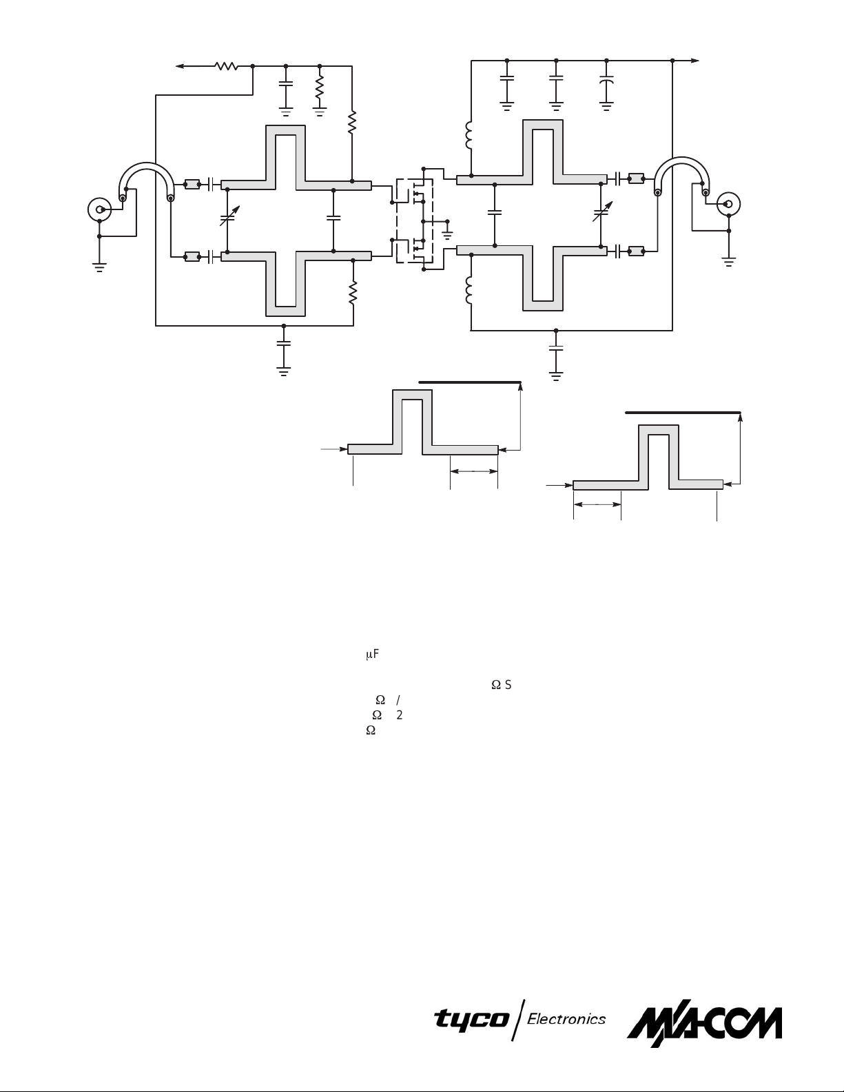
BIAS SUPPLY
R1
C11
R2
C12 C14
C13
+
–
VDD = 28 Vdc
RF INPUT
B1
C2
C1
C3
C9
C4
C3
R3
R4
L1
D.U.T.
L2
Inputs Line
70 mils x 2460 mils
C4
490 mils
C5
C6
C10
C5
680 mils
C7
C8
Output Lines
70 mils x 2380 mils
B2
RF OUTPUT
C6
C1, C2, C7, C8 220 pF, 100 mil Chip Capacitor, ATC
C3, C6 0 – 10 pF, Johanson
C4 27 pF, 100 mil Chip Capacitor, ATC
C5 22 pF, 100 mil Chip Capacitor, ATC
C9, C10, C1 1, C12 0.01 µF Blue Capacitor
C13 470 pF, 100 mil Chip Capacitor, ATC
C14 50 mF, 50 V Electrolytic Capacitor
L1, L2 8 Turns #20 A WG, 0.100 mils ID
B1, B2 6″ long, ID = 550 mils, 50 W Semi–Rigid Coax
R1 1.0 kW 1/2 Watt
R2 10 kW 1/2 Watt
R3, R4 45 W 1/2 Watt
Board Material – Teflon
Dielectric Thickness = 0.30″,
Fiberglass
εr = 2.55 Copper Clad, 2.0 oz. Copper
Figure 1. MRF166W 500 MHz T est Circuit Schematic
REV 3
3
Page 4

60
55
50
45
40
35
30
25
20
, OUTPUT POWER (WATTS)
15
out
P
10
5
0
f = 500 MHz
VDD = 28 Vdc
IDQ = 100 mA
0 1 1.5 2 3
0.5 2.5
Pin, INPUT POWER (WA TTS)
24
f = 500 MHz
0 0.4 1.2 2
Pin, INPUT POWER (WA TTS)
, OUTPUT POWER (WATTS)
out
P
20
16
12
8
4
0
VDD = 13.5 Vdc
IDQ = 100 mA
2.4 2.80.8 1.6
Figure 2. Output Power versus Input Power, 28 Vdc
56
52
12
IDQ = 100 mA
f = 500 MHz
14
16 18 20 22 24 26 28
VDD, SUPPLY VOLTAGE (VOLTS)
Pin = 2 W
Pin = 1 W
Pin = 0.5 W
, OUTPUT POWER (WATTS)
out
P
48
44
40
36
32
28
24
20
16
12
8
Figure 4. Output Power versus Supply Voltage
Figure 3. Output Power versus Input Power, 13.5
Vdc
45
40
VDD = 28 Vdc
IDQ = 100 mA
35
30
25
20
TYPICAL DEVICE SHOWN
15
V
= 3.0 V
, OUTPUT POWER (WATTS)
out
P
10
GS(th)
5
0
–5 –4 –2 0
VDS, GATE–SOURCE VOLTAGE (VOLTS)
f = 500 MHz
1–3 –1
Figure 5. Output Power versus Gate Voltage
2
3
REV 3
4
100
90
80
70
60
50
40
30
C, CAPACITANCE (pF)
20
10
0
0 4 12 20
C
oss
C
iss
C
rss
VDS, DRAIN–SOURCE VOLTAGE (VOLTS)
Figure 6. Capacitance versus V oltage
VGS = 0 V
f = 1.0 MHz
24816
28
Page 5

175
400
Z
in
ZOL*
500
f = 175 MHz
400
f = 500 MHz
Zo = 50 Ω
VDD = 28 Vdc, IDQ = 100 mA, P
f
MHz
175 3.7 – j 22.4 15.2 – j 16.6
400 3.6 – j 10.99 10.3 – j 7.99
500 2.88 – j 7.96 6.12 – j 9.43
Z
in
Ohms
out
= 40 W
ZOL*
Ohms
T able 1. Input and Output Impedances
Figure 7. Series Equivalent Input/Output Impedance
ZOL* = Conjugate of the optimum load impedance into which the device
output operates at a given output power, voltage and frequency.
NOTE: Input and output impedance values given are measured from gate to
gate and drain to drain respectively.
REV 3
5
Page 6

MRF166W–500MHZ M J B
NOTES: 1) 3 X 5 inch Glass Teflon 32 Mil Board, Copper Both Sides
NOTES: 2) Small Holes are 40 Mils ID and Plated Through
NOTES: 3) Large Holes are 140 Mils ID and Plated Through
Figure 8. MRF166W Circuit Board Photomaster
(Scale 1:1)
REV 3
6
Figure 9. MRF166W T est Fixture
Page 7

f
MHz
30
40
50
60
70
80
90
100
110
120
130
140
150
160
170
180
190
200
210
220
230
240
250
260
270
280
290
300
310
320
330
340
350
360
370
380
390
400
410
420
430
440
T able 1. Common Source S–Parameters (VDS = 24 V, ID = 230 mA)
S
11
|S11| φ |S21| φ |S12| φ |S22| φ
0.554
0.775
0.758
0.711
0.751
0.742
0.724
0.730
0.735
0.732
0.734
0.740
0.747
0.748
0.741
0.746
0.753
0.756
0.755
0.759
0.767
0.769
0.766
0.767
0.773
0.777
0.777
0.782
0.788
0.794
0.796
0.795
0.799
0.804
0.805
0.807
0.812
0.818
0.821
0.821
0.822
0.826
–85
–113
–124
–132
–139
–143
–146
–149
–151
–153
–155
–156
–157
–159
–160
–160
–161
–162
–162
–163
–163
–164
–164
–165
–165
–165
–166
–166
–166
–167
–167
–168
–168
–168
–168
–169
–169
–170
–170
–170
–171
–171
20.30
20.00
17.50
14.60
12.70
11.30
10.00
8.97
8.29
7.53
7.01
6.57
6.01
5.66
5.22
4.94
4.67
4.51
4.15
3.91
3.75
3.56
3.41
3.26
3.07
3.03
2.89
2.80
2.66
2.54
2.47
2.38
2.27
2.17
2.15
2.06
2.00
1.91
1.86
1.83
1.74
1.67
S
21
128
113
107
100
100
95
92
90
87
84
83
81
78
76
76
74
73
70
69
68
65
64
63
63
61
61
58
57
57
55
54
54
52
51
50
48
48
47
46
44
44
43
0.044
0.040
0.041
0.050
0.042
0.043
0.042
0.042
0.043
0.042
0.042
0.043
0.042
0.041
0.040
0.041
0.041
0.040
0.039
0.039
0.039
0.038
0.037
0.035
0.035
0.035
0.034
0.034
0.034
0.033
0.032
0.031
0.030
0.030
0.030
0.029
0.028
0.027
0.029
0.028
0.026
0.025
S
12
28
26
20
20
11
9
8
6
3
2
1
0
–2
–4
–4
–4
–6
–7
–8
–8
–10
–12
–12
–10
–10
–11
–13
–11
–12
–12
–13
–13
–11
–11
–11
–12
–12
–10
–11
–11
–9
–7
0.628
0.632
0.652
0.570
0.666
0.666
0.657
0.663
0.683
0.666
0.688
0.701
0.688
0.715
0.690
0.719
0.725
0.729
0.727
0.724
0.751
0.733
0.726
0.725
0.725
0.753
0.732
0.744
0.764
0.760
0.787
0.753
0.772
0.782
0.796
0.782
0.796
0.784
0.830
0.823
0.791
0.788
S
22
–121
–123
–135
–135
–145
–149
–151
–154
–156
–158
–159
–160
–162
–162
–161
–164
–165
–166
–165
–166
–169
–167
–167
–167
–167
–167
–169
–169
–169
–167
–169
–170
–168
–169
–169
–170
–170
–168
–170
–171
–170
–170
REV 3
7
Page 8

f
f
f
MHz
MHz
450
460
470
480
490
500
600
700
800
900
1000
MHz
30
40
50
60
70
80
90
100
110
120
130
140
150
160
170
180
190
200
210
220
230
240
250
260
270
280
290
300
T able 1. Common Source S–Parameters (VDS = 24 V, ID = 230 mA) (continued)
S
22
–170
–174
–173
–172
–171
–172
–176
–177
178
179
174
0.830
0.831
0.832
0.835
0.835
0.823
0.874
0.910
0.932
0.966
0.975
S
12
–7
–10
–7
–3
1
3
–171
89
61
68
49
0.820
0.843
0.827
0.836
0.835
0.849
0.873
0.867
0.904
0.897
0.953
1.68
1.64
1.54
1.50
1.43
1.43
1.12
0.86
0.74
0.63
0.54
S
21
42
41
41
39
38
37
29
23
18
12
5
0.025
0.026
0.025
0.024
0.024
0.025
0.003
0.013
0.035
0.029
0.042
S
11
–171
–172
–172
–173
–173
–174
–176
–179
179
176
172
T able 2. Common Source S–Parameters (VDS = 28 V, ID = 250 mA)
S
11
|S11| φ |S21| φ |S12| φ |S22| φ
0.601
0.783
0.764
0.727
0.759
0.751
0.732
0.737
0.741
0.738
0.740
0.747
0.754
0.757
0.749
0.753
0.759
0.761
0.759
0.762
0.771
0.775
0.774
0.775
0.780
0.782
0.781
0.785
–86
–112
–122
–131
–138
–142
–146
–149
–150
–153
–154
–156
–157
–159
–159
–160
–161
–161
–162
–163
–164
–164
–165
–165
–165
–165
–166
–166
22.20
21.20
18.50
15.50
13.50
12.10
10.70
9.55
8.81
8.01
7.47
7.01
6.43
6.07
5.59
5.28
4.99
4.81
4.44
4.18
4.03
3.83
3.69
3.52
3.29
3.24
3.10
3.01
S
21
128
114
108
101
100
95
93
90
88
85
83
82
79
77
76
75
73
70
70
69
66
65
64
63
61
61
59
58
0.040
0.037
0.038
0.045
0.039
0.040
0.040
0.040
0.040
0.040
0.040
0.040
0.040
0.039
0.038
0.039
0.039
0.038
0.037
0.037
0.037
0.036
0.035
0.034
0.034
0.034
0.032
0.033
S
12
29
27
21
21
12
9
8
6
4
3
2
1
–2
–3
–3
–4
–5
–7
–6
–7
–9
–10
–10
–10
–10
–11
–12
–11
0.796
0.616
0.637
0.574
0.648
0.649
0.641
0.648
0.670
0.654
0.675
0.684
0.669
0.693
0.670
0.701
0.712
0.719
0.713
0.709
0.733
0.715
0.713
0.715
0.712
0.741
0.722
0.733
S
22
–119
–122
–133
–135
–143
–148
–150
–153
–155
–156
–157
–158
–161
–161
–161
–163
–164
–165
–163
–164
–167
–165
–166
–168
–168
–168
–168
–168
φ|S22|φ|S12|φ|S21|φ|S11|
REV 3
8
Page 9

f
f
MHz
MHz
310
320
330
340
350
360
370
380
390
400
410
420
430
440
450
460
470
480
490
500
600
700
800
900
1000
T able 2. Common Source S–Parameters (VDS = 28 V, ID = 250 mA) (continued)
S
12
–12
–12
–13
–14
–12
–12
–12
–13
–13
–11
–12
–13
–12
–11
–10
–13
–11
–10
–10
–10
138
77
58
69
49
0.792
0.798
0.801
0.800
0.803
0.807
0.808
0.809
0.813
0.820
0.823
0.823
0.824
0.828
0.832
0.833
0.835
0.840
0.844
0.845
0.879
0.912
0.935
0.966
0.974
2.87
2.75
2.68
2.58
2.44
2.33
2.30
2.19
2.14
2.06
2.02
1.98
1.89
1.83
1.81
1.75
1.65
1.60
1.55
1.56
1.21
0.92
0.79
0.67
0.57
S
21
57
56
53
53
52
50
50
48
49
47
45
44
44
43
41
41
41
40
38
37
29
23
18
11
5
0.032
0.032
0.031
0.030
0.029
0.029
0.029
0.028
0.027
0.026
0.027
0.026
0.025
0.024
0.024
0.025
0.023
0.022
0.022
0.022
0.002
0.017
0.039
0.030
0.043
S
11
–167
–167
–168
–168
–169
–169
–169
–169
–170
–170
–170
–171
–171
–172
–172
–172
–172
–172
–173
–173
–176
–179
179
176
172
0.750
0.739
0.760
0.727
0.755
0.772
0.787
0.768
0.775
0.765
0.805
0.794
0.778
0.785
0.812
0.838
0.817
0.818
0.819
0.833
0.870
0.862
0.887
0.892
0.945
S
22
φ|S22|φ|S12|φ|S21|φ|S11|
–167
–166
–170
–172
–170
–171
–169
–170
–169
–167
–170
–173
–174
–173
–172
–175
–173
–172
–172
–173
–176
–176
179
179
175
REV 3
9
Page 10

P ACKAGE DIMENSIONS
–A–
U
G
12
K
345
–B–
Q
2 PL
0.51 (0.020) B
M
M
A
T
M
D 4 PL
T
M
A
SEATING
PLANE
M
0.51 (0.020) B
J
N
E
H
M
C
–T–
NOTES:
1. DIMENSIONING AND TOLERANCING
PER ANSI Y14.5M, 1982.
2. CONTROLLING DIMENSION: INCH.
DIM MIN MAX MIN MAX
A 0.965 0.985 24.52 25.01
B 0.245 0.265 6.23 6.73
C 0.165 0.185 4.20 4.69
D 0.050 0.070 1.27 1.77
E 0.070 0.080 1.78 2.03
G 0.254 BSC 6.45 BSC
H 0.095 0.105 2.42 2.66
J 0.003 0.006 0.08 0.15
K 0.625 0.675 15.88 17.14
N 0.495 0.520 12.58 13.20
Q 0.120 0.140 3.05 3.55
U 0.725 BSC 18.42 BSC
STYLE 1:
PIN 1. DRAIN
2. DRAIN
3. GATE
4. GATE
5. SOURCE
MILLIMETERSINCHES
CASE 412–01
ISSUE O
Specifications subject to change without notice.
n
North America: Tel. (800) 366-2266, Fax (800) 618-8883
n Asia/Pacific: Tel.+81-44-844-8296, Fax +81-44-844-8298
n
Europe: Tel. +44 (1344) 869 595, Fax+44 (1344) 300 020
Visit www.macom.com for additional data sheets and product information.
REV 3
10
 Loading...