

Page 1
SEMICONDUCTOR TECHNICAL DATA
The RF Line
RF Power Transistor
Designed for 28 Volt microwave large–signal, common base, Class–C CW
amplifier applications in the range 1600 – 1640 MHz.
• Specified 28 Volt, 1.6 GHz Class–C Characteristics
Output Power = 30 Watts
Minimum Gain = 7.5 dB, @ 30 Watts
Minimum Efficiency = 40% @ 30 Watts
• Characterized with Series Equivalent Large–Signal Parameters from
1500 MHz to 1700 MHz
• Silicon Nitride Passivated
• Gold Metallized, Emitter Ballasted for Long Life and Resistance to Metal
Migration
Order this document
by MRF16030/D
30 WATTS, 1.6 GHz
RF POWER TRANSISTOR
NPN SILICON
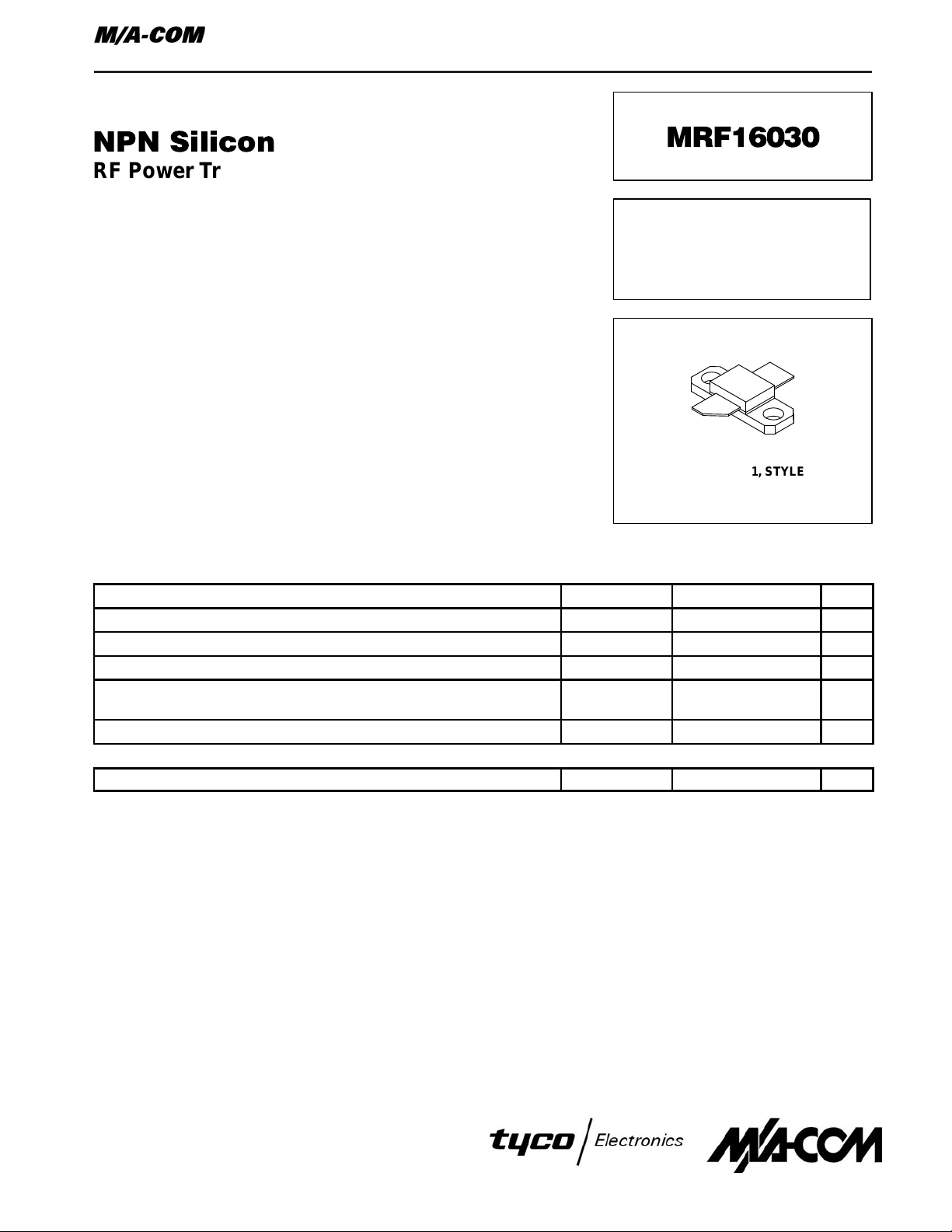
CASE 395C–01, STYLE 2
MAXIMUM RATINGS
Collector–Emitter Voltage V
Emitter–Base Voltage V
Collector–Current I
Total Device Dissipation @ TC = 25°C
Derate above 25°C
Storage Temperature Range T
(TJ = 25°C unless otherwise noted)
Rating
Symbol Value Unit
CES
EBO
C
P
D
stg
–65 to +150 °C
THERMAL CHARACTERISTICS
Thermal Resistance — Junction to Case (1) (2) R
(1) Thermal measurement performed using CW RF operating condition.
(2) Thermal resistance is determined under specified RF operating conditions by infrared measurement techniques.
θJC
60 Vdc
4.0 Vdc
4.0 Adc
103
0.58
1.7 °C/W
Watts
°C/W
REV 3
1
Page 2
ELECTRICAL CHARACTERISTICS (T
Characteristic Symbol Min Typ Max Unit
OFF CHARACTERISTICS
Collector–Emitter Breakdown V oltage
(IC = 100 mAdc, VBE = 0)
Collector–Base Breakdown Voltage
(IC = 100 mAdc, IE = 0)
Emitter–Base Breakdown Voltage
(IE = 10 mAdc, IC = 0)
Collector Cutoff Current
(VCE = 28 Vdc, VBE = 0)
ON CHARACTERISTICS
DC Current Gain
(ICE = 1.0 Adc, VCE = 5.0 Vdc)
FUNCTIONAL TESTS
Collector–Base Amplifier Power Gain
(VCC = 28 Vdc, P
Collector Efficiency
(VCC = 28 Vdc, P
Input Return Loss
(VCC = 28 Vdc, P
Output Mismatch Stress
VCC = 28 Vdc, P
VSWR = 3:1, All phase angles at frequency of test
= 30 Watts, f = 1600/1640 MHz)
out
= 30 Watts, f = 1600/1640 MHz)
out
= 30 Watts, f = 1600/1640 MHz)
out
= 30 Watts, f = 1600 MHz, Load
out
= 25°C unless otherwise noted)
C
V
(BR)CES
V
(BR)CBO
V
(BR)EBO
I
CES
h
FE
G
pe
η
I
RL
Ψ
55 — —
55 — —
4.0
— —
— — 10
20 35 80
7.5 7.7 —
40 45 —
8.0 — —
No Degradation in Output Power
Vdc
Vdc
Vdc
mAdc
—
dB
%
dB
REV 3
2
Page 3

L3
Board Material – Teflon Glass Laminate Dielectric
Thickness = 0.30
B1 Fair Rite Bead on #24 Wire
C1, C5 100 pF, B Case, ATC Chip Cap
C2 0.1 µF, Dipped Mica Cap
C3 0.1 µF, Chip Cap
L2
L1
″, εr = 2.55″, 2.0 oz. Copper
B1
C1 C2 C4C3
R1
28 Vdc
C5
C4 47 µF, 50 V, Electrolytic
L1, L2 3 Turns, #18, 0.133″ ID, 0.15″ Long
L3 9 Turns, #24 Enamel
R1 82 Ω, 1.0 W, Carbon
Figure 1. MRF16030 T est Fixture Schematic
f = 1.5 GHz
Z
f = 1.5 GHz
ZOL*
Ohms
f
MHz
1.7 GHz
ZOL*
VCC = 28 Vdc, P
Zin
Ohms
1.6 GHz
= 30 W
out
1500 3.05 + j 4.88 2.66 + j 2.53
1600 4.32 + j 6.00 1.79 + j 2.80
1700 5.62 + j 5.79 1.51 + j 2.64
in
1.6 GHz
1.7 GHz
Zo = 10
Ω
ZOL* = Conjugate of the optimum load impedance into which the device
output operates at a given output power, voltage and frequency.
REV 3
3
Figure 2. Series Equivalent Input/Output Impedance
Page 4

45
40
f = 1.6 GHz
35
30
25
, OUTPUT POWER (WATTS)
out
P
20
15
4.0 4.5 5.5 6.5 7.5 8.5 9.0
Pin, INPUT POWER (WATTS)
1.64 GHz
VCC = 28 Vdc
7.0 8.05.0 6.0
Figure 3. Output Power versus Input Power
REV 3
4
Page 5

P ACKAGE DIMENSIONS
–A–
U
1
–B–
3
K
2
D
N
E
J
H
2 PLQ
0.51 (0.020) B
M
T
C
SEATING
–T–
PLANE
M
A
M
NOTES:
1. DIMENSIONING AND TOLERANCING PER ANSI
Y14.5M, 1982.
2. CONTROLLING DIMENSION: INCH.
INCHES
DIMAMIN MAX MIN MAX
0.739 0.750 18.77 19.05
B 0.240 0.260 6.10 6.60
C 0.165 0.198 4.19 5.03
D 0.215 0.225 5.46 5.72
E 0.055 0.070 1.40 1.78
H 0.079 0.091 2.01 2.31
J 0.004 0.006 0.10 0.15
K 0.210 0.240 5.33 6.10
N 0.315 0.330 8.00 8.38
Q 0.125 0.135 3.18 3.42
U 0.560 BSC 14.23 BSC
STYLE 2:
PIN 1. EMITTER
2. COLLECTOR
3. BASE
MILLIMETERS
CASE 395C–01
ISSUE A
Specifications subject to change without notice.
n
North America: Tel. (800) 366-2266, Fax (800) 618-8883
n Asia/Pacific: Tel.+81-44-844-8296, Fax +81-44-844-8298
n
Europe: Tel. +44 (1344) 869 595, Fax+44 (1344) 300 020
Visit www.macom.com for additional data sheets and product information.
REV 3
5
 Loading...