

Page 1
SEMICONDUCTOR TECHNICAL DATA
The RF MOSFET Line
RFPowerField-EffectTransistor
N–Channel Enhancement–Mode MOSFET
Designed for broadband commercial and military applications at frequencies
to 175 MHz. The high power, high gain and broadband performance of this
device makes possible solid state transmitters for FM broadcast or TV channel
frequency bands.
•Guaranteed Performance at 175 MHz, 50 V:
Output Power — 300 W
Gain — 14 dB (16 dB Typ)
Efficiency — 50%
•Low Thermal Resistance — 0.35°C/W
•Ruggedness Tested at Rated Output Power
•Nitride Passivated Die for Enhanced Reliability
D
Order this document
by MRF151G/D
MRF151G
300 W, 50 V, 175 MHz
N–CHANNEL
BROADBAND
RF POWER MOSFET
G
G
D
(FLANGE)
MAXIMUM RATINGS
Rating Symbol Value Unit
Drain–Source Voltage V
Drain–Gate Voltage V
Gate–Source Voltage V
Drain Current — Continuous I
Total Device Dissipation @ TC = 25°C
Derate above 25°C
Storage Temperature Range T
Operating Junction Temperature T
THERMAL CHARACTERISTICS
Characteristic Symbol Max Unit
Thermal Resistance, Junction to Case R
S
CASE 375–04, STYLE 2
DSS
DGO
GS
D
P
D
stg
J
θ
JC
125 Vdc
125 Vdc
±40 Vdc
40 Adc
500
2.85
–65 to +150 °C
200 °C
0.35 °C/W
Watts
W/°C
NOTE — CAUTION — MOS devices are susceptible to damage from electrostatic charge. Reasonable precautions in handling and
packaging MOS devices should be observed.
REV 9
1
Page 2
ELECTRICAL CHARACTERISTICS (T
= 25°C unless otherwise noted.)
C
Characteristic Symbol Min Typ Max Unit
OFF CHARACTERISTICS (Each Side)
Drain–Source Breakdown Voltage (VGS = 0, ID = 100 mA) V
Zero Gate Voltage Drain Current (VDS = 50 V, VGS = 0) I
Gate–Body Leakage Current (VGS = 20 V, VDS = 0) I
ON CHARACTERISTICS (Each Side)
Gate Threshold Voltage (VDS = 10 V, ID = 100 mA) V
Drain–Source On–Voltage (VGS = 10 V, ID = 10 A) V
Forward Transconductance (VDS = 10 V, ID = 5.0 A) g
DYNAMIC CHARACTERISTICS (Each Side)
Input Capacitance (VDS = 50 V, VGS = 0, f = 1.0 MHz) C
Output Capacitance (VDS = 50 V, VGS = 0, f = 1.0 MHz) C
Reverse Transfer Capacitance (VDS = 50 V, VGS = 0, f = 1.0 MHz) C
FUNCTIONAL TESTS
Common Source Amplifier Power Gain
(V
= 50 V, P
DD
Drain Efficiency
(V
= 50 V, P
DD
Load Mismatch
(V
= 50 V, P
DD
VSWR 5:1 at all Phase Angles)
= 300 W, IDQ = 500 mA, f = 175 MHz)
out
= 300 W, f = 175 MHz, ID (Max) = 11 A)
out
= 300 W, IDQ = 500 mA,
out
(BR)DSS
DSS
GSS
GS(th)
DS(on)
fs
iss
oss
rss
G
ps
125 — — Vdc
— — 5.0 mAdc
— — 1.0 µAdc
1.0 3.0 5.0 Vdc
1.0 3.0 5.0 Vdc
5.0 7.0 — mhos
— 350 — pF
— 220 — pF
— 15 — pF
14 16 — dB
η 50 55 — %
ψ
No Degradation in Output Power
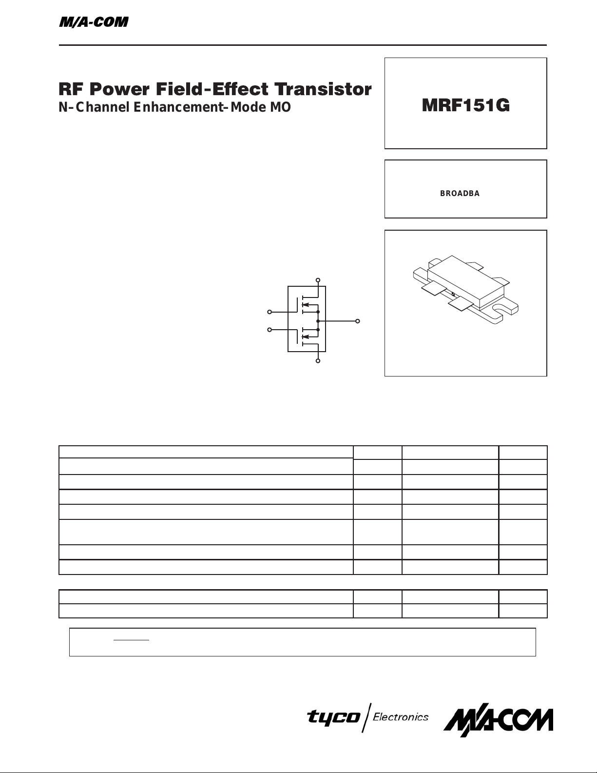
+
BIAS 0–6 V
R1
C5C4
–
R2
C1
INPUT
C1
T1
C6
C2
C3
R1 — 100 Ohms, 1/2 W
R2 — 1.0 kOhm, 1/2 W
C1 — Arco 424
C2 — Arco 404
C3, C4, C7, C8, C9 — 1000 pF Chip
C5, C10 — 0.1 µF Chip
C6 — 330 pF Chip
C11 — 0.47 µF Ceramic Chip, Kemet 1215 or
C11 — Equivalent (100 V)
C12 — Arco 422
L1 — 10 Turns AWG #18 Enameled Wire,
L1 — Close Wound, 1/4″ I.D.
L2 — Ferrite Beads of Suitable Material for
L2 — 1.5–2.0 µH Total Inductance
Unless Otherwise Noted, All Chip Capacitors are ATC Type 100 or
Equivalent.
Figure 1. 175 MHz Test Circuit
L2
C10C9
L1
D.U.T.
T2
C7 C8
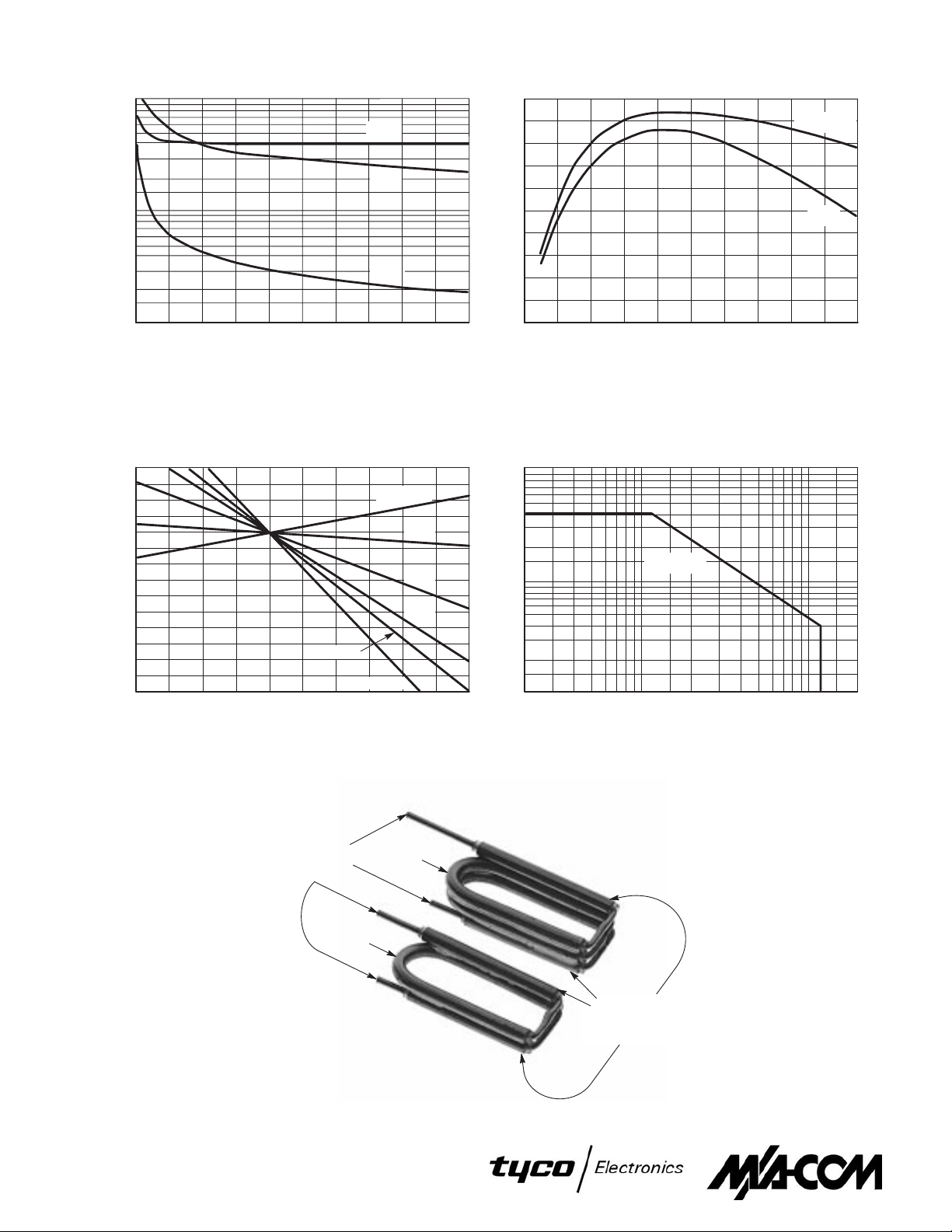
T1 — 9:1 RF Transformer. Can be made of 15–18 Ohms
T1 — Semirigid Co–Ax, 62–90 Mils O.D.
T2 — 1:4 RF Transformer. Can be made of 16–18 Ohms
T2 — Semirigid Co–Ax, 70–90 Mils O.D.
Board Material — 0.062″ Fiberglass (G10),
1 oz. Copper Clad, 2 Sides, ε
= 5.0
r
NOTE: For stability, the input transformer T1 must be loaded
NOTE: with ferrite toroids or beads to increase the common
NOTE: mode inductance. For operation below 100 MHz. The
NOTE: same is required for the output transformer.
See Figure 6 for construction details of T1 and T2.
C11
C12
+
50 V
–
OUTPUT
REV 9
2
Page 3
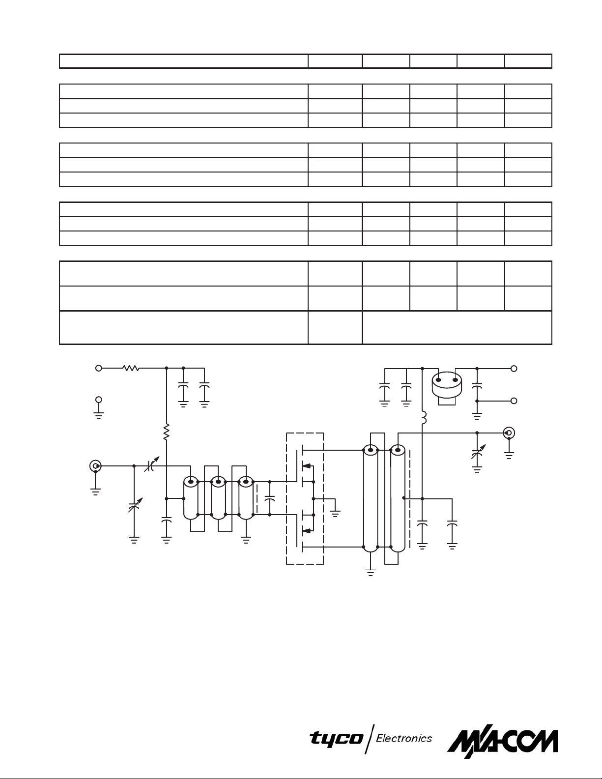
TYPICAL CHARACTERISTICS
1000
C
500
200
100
50
C, CAPACITANCE (pF)
20
0
0 1020304050
VDS, DRAIN–SOURCE VOLTAGE (VOLTS)
iss
C
oss
C
rss
Figure 2. Capacitance versus
Drain–Source Voltage*
*Data shown applies to each half of MRF151G.
1.04
1.03
1.02
1.01
1
0.99
0.98
0.97
0.96
0.95
0.94
0.93
0.92
, DRAIN-SOURCE VOLTAGE (NORMALIZED)
0.91
GS
0.9
V
–25 0 25 50 75 100
, CASE TEMPERATURE (°C)
T
C
250 mA
ID = 5 A
4 A
2 A
1 A
100 mA
2000
VDS = 30 V
1000
, UNITY GAIN FREQUENCY (MHz)
T
f
0
048121620
2 6 10 14 18
I
, DRAIN CURRENT (AMPS)
D
15 V
Figure 3. Common Source Unity Gain Frequency
versus Drain Current*
100
TC = 25°C
10
, DRAIN CURRENT (AMPS)
D
I
1
2 20 200
, DRAIN–TO–SOURCE VOLTAGE (VOL TS)
V
DS
REV 9
3
Figure 4. Gate–Source V oltage versus
Case T emperature*
HIGH IMPEDANCE
WINDINGS
CENTER
CENTER
TAP
TAP
IMPEDANCE
Figure 6. RF Transformer
4:1
RATIO
Figure 5. DC Safe Operating Area
9:1
IMPEDANCE
RATIO
CONNECTIONS
TO LOW IMPEDANCE
WINDINGS
Page 4

TYPICAL CHARACTERISTICS
350
300
f = 150 MHz
175 MHz
200 MHz
30
25
250
200
150
, OUTPUT POWER (WATTS)
100
out
P
VDD = 50 V
I
= 2 x 250 mA
DQ
20
15
, POWER GAIN (dB)
PS
G
10
VDD = 50 V
I
DQ
P
out
50
0
0510
5
2 5 10 30 100 200
Pin, INPUT POWER (WA TTS)
Figure 7. Output Power versus Input Power Figure 8. Power Gain versus Frequency
= 2 x 250 mA
= 150 W
f, FREQUENCY (MHz)
f = 175 MHz
150
125
INPUT, Z
100
(GATE TO GATE)
in
Zo = 10 Ω
30
150
125
100
30
f = 175 MHz
OUTPUT, ZOL*
(DRAIN TO DRAIN)
Z
* = Conjugate of the optimum load impedance
OL
Z
* = into which the device output operates at a
OL
* = given output power, voltage and frequency.
Z
OL
Figure 9. Input and Output Impedance
REV 9
4
Page 5

NOTE: S–Parameter data represents measurements taken from one chip only.
f
T able 1. Common Source S–Parameters (VDS = 50 V, ID = 2 A)
MHz
30
40
50
60
70
80
90
100
110
120
130
140
150
160
170
180
190
200
210
220
230
240
250
260
270
280
290
300
310
320
330
340
350
360
370
380
390
400
410
420
S
11
S
21
S
12
S
22
|S11| φ |S21| φ |S12| φ |S22| φ
0.877
0.886
0.895
0.902
0.912
0.918
0.925
0.932
0.936
0.942
0.946
0.950
0.954
0.957
0.960
0.962
0.964
0.967
0.967
0.969
0.971
0.970
0.972
0.973
0.972
0.974
0.974
0.975
0.976
0.974
0.975
0.976
0.975
0.977
0.976
0.976
0.977
0.976
0.976
0.977
–174
–175
–175
–176
–176
–177
–177
–177
–178
–178
–179
–179
–180
–180
180
179
179
179
178
178
178
177
177
177
176
176
176
176
175
175
174
174
174
174
173
173
173
172
172
172
10.10
7.47
5.76
4.73
3.86
3.19
2.69
2.34
2.06
1.77
1.55
1.39
1.23
1.13
1.01
0.90
0.84
0.75
0.71
0.67
0.60
0.57
0.51
0.47
0.45
0.41
0.40
0.39
0.36
0.33
0.31
0.30
0.29
0.28
0.26
0.26
0.24
0.23
0.22
0.21
77
69
63
58
52
48
45
40
37
35
32
30
27
24
22
20
19
18
16
14
12
12
12
11
10
10
10
0.008
0.009
0.008
0.009
0.009
0.010
0.011
0.013
0.014
0.015
0.017
0.019
0.021
0.023
0.024
0.026
0.028
0.030
0.032
0.035
0.038
0.037
0.039
0.041
9
9
6
0.044
0.046
0.046
0.048
9
7
4
0.049
0.053
0.056
0.056
7
8
8
7
0.058
0.059
0.061
0.065
0.066
7
9
9
0.068
0.071
0.071
19
24
33
39
46
54
62
67
72
76
77
77
78
79
82
82
80
79
80
82
81
80
80
79
80
80
79
82
82
78
78
77
80
79
76
75
76
80
77
76
0.707
0.715
0.756
0.764
0.784
0.802
0.808
0.850
0.865
0.875
0.874
0.884
0.909
0.911
0.904
0.931
0.929
0.922
0.937
0.949
0.950
0.950
0.935
0.954
0.953
0.965
0.944
0.929
0.943
0.954
0.935
0.948
0.950
0.978
0.981
0.944
0.960
0.955
0.999
0.962
–169
–172
–171
–171
–172
–171
–171
–173
–175
–173
–172
–174
–175
–176
–177
–176
–178
–179
–180
180
179
179
179
178
176
175
175
176
176
173
172
172
174
172
170
171
171
173
170
168
REV 9
5
Page 6

f
MHz
f
430
440
450
460
470
480
490
500
MHz
30
40
50
60
70
80
90
100
110
120
130
140
150
160
170
180
190
200
210
220
230
240
250
260
270
280
290
300
310
320
330
T able 1. Common Source S–Parameters (VDS = 50 V, ID = 2 A) continued
S
11
|S11| φ |S21| φ |S12| φ |S22| φ
0.976
0.976
0.978
0.978
0.978
0.974
0.973
0.972
171
171
171
170
170
170
169
169
0.19
0.20
0.19
0.18
0.18
0.18
0.17
0.17
S
21
10
12
10
13
10
13
13
14
0.073
0.075
0.080
0.082
0.081
0.085
0.086
0.089
S
12
76
75
77
74
77
78
75
73
0.950
0.953
0.982
0.990
0.953
0.944
0.966
0.980
S
22
168
168
168
165
168
167
165
165
T able 2. Common Source S–Parameters (VDS = 50 V, ID = 0.38 A)
S
11
|S11| φ |S21| φ |S12| φ |S22| φ
0.834
0.869
0.883
0.892
0.901
0.911
0.924
0.935
0.945
0.953
0.958
0.962
0.964
0.966
0.969
0.972
0.975
0.977
0.979
0.980
0.980
0.981
0.982
0.983
0.984
0.984
0.984
0.984
0.984
0.985
0.985
–168
–169
–170
–171
–172
–173
–173
–174
–174
–175
–175
–176
–177
–177
–178
–178
–178
–179
–179
–179
–180
180
180
179
179
179
178
178
178
177
177
9.70
6.47
5.13
4.03
3.39
2.80
2.39
1.99
1.67
1.36
1.14
1.01
0.93
0.85
0.79
0.74
0.65
0.56
0.50
0.44
0.41
0.38
0.38
0.34
0.34
0.30
0.27
0.25
0.24
0.23
0.20
S
21
74
62
55
51
50
47
42
35
29
25
23
23
24
24
21
17
10
8
7
9
9
12
11
8
4
3
–4
0
4
7
3
0.014
0.013
0.012
0.011
0.010
0.009
0.008
0.006
0.005
0.004
0.004
0.004
0.004
0.004
0.005
0.006
0.007
0.008
0.008
0.008
0.009
0.009
0.011
0.014
0.014
0.013
0.012
0.014
0.017
0.019
0.019
S
12
–10
–19
–24
–24
–20
–16
–14
–15
–17
–10
4
26
45
58
61
57
56
63
72
81
79
74
74
76
80
79
73
69
74
83
90
0.747
0.731
0.754
0.823
0.912
0.996
1.100
1.100
1.070
0.988
0.934
0.935
0.983
1.080
1.170
1.250
1.210
1.110
1.010
0.958
1.020
1.020
1.060
1.180
1.220
1.180
1.040
0.996
0.951
0.964
1.060
S
22
–162
–159
–161
–164
–167
–168
–167
–167
–169
–167
–169
–170
–172
–173
–173
–173
–174
–174
–174
–172
–175
–178
–176
–179
–180
–179
–177
–178
–178
179
180
REV 9
6
Page 7

f
MHz
340
350
360
370
380
390
400
410
420
430
440
450
460
470
480
490
500
T able 2. Common Source S–Parameters (V
S
11
S
21
= 50 V, ID = 0.38 A) continued
DS
S
12
S
22
|S11| φ |S21| φ |S12| φ |S22| φ
0.986
0.986
0.986
0.985
0.985
0.985
0.985
0.985
0.986
0.986
0.986
0.985
0.984
0.984
0.985
0.986
0.986
177
177
176
176
176
176
175
175
175
174
174
174
174
174
173
173
173
0.22
0.20
0.19
0.17
0.16
0.15
0.14
0.14
0.13
0.13
0.13
0.13
0.11
0.10
0.10
0.10
0.10
–2
–3
–3
–1
–2
–1
7
5
0
3
2
5
4
0
3
1
6
0.017
0.017
0.021
0.024
0.024
0.021
0.018
0.021
0.027
0.031
0.030
0.025
0.022
0.025
0.034
0.038
0.035
87
76
67
69
77
85
85
72
68
73
81
87
68
59
66
79
93
1.100
1.140
1.160
1.100
1.070
0.993
0.962
1.040
1.060
1.100
1.140
1.110
1.090
1.020
0.993
1.020
1.010
179
–180
180
180
–180
–180
–180
179
177
177
177
178
176
177
179
178
177
REV 9
7
Page 8

RF POWER MOSFET CONSIDERA TIONS
MOSFET CAPACITANCES
The physical structure of a MOSFET results in capacitors
between the terminals. The metal anode gate structure determines the capacitors from gate–to–drain (C
to–source (C
). The PN junction formed during the
gs
), and gate–
gd
fabrication of the RF MOSFET results in a junction capacitance from drain–to–source (C
These capacitances are characterized as input (C
put (C
) and reverse transfer (C
oss
).
ds
) capacitances on data
rss
iss
), out-
sheets. The relationships between the inter–terminal capacitances and those given on data sheets are shown below. The
C
can be specified in two ways:
iss
1. Drain shorted to source and positive voltage at the gate.
2. Positive voltage of the drain in respect to source and zero
volts at the gate. In the latter case the numbers are lower.
However, neither method represents the actual operating conditions in RF applications.
DRAIN
C
ds
SOURCE
C
iss
C
oss
C
rss
= Cgd = C
= Cgd = C
= C
gd
gs
ds
GATE
C
gd
C
gs
LINEARITY AND GAIN CHARACTERISTICS
In addition to the typical IMD and power gain data presented, Figure 3 may give the designer additional information
on the capabilities of this device. The graph represents the
small signal unity current gain frequency at a given drain current level. This is equivalent to f
for bipolar transistors.
T
Since this test is performed at a fast sweep speed, heating of
the device does not occur. Thus, in normal use, the higher
temperatures may degrade these characteristics to some extent.
DRAIN CHARACTERISTICS
One figure of merit for a FET is its static resistance in the
full–on condition. This on–resistance, V
, occurs in the
DS(on)
linear region of the output characteristic and is specified under specific test conditions for gate–source voltage and drain
current. For MOSFETs, V
has a positive temperature
DS(on)
coefficient and constitutes an important design consideration
at high temperatures, because it contributes to the power
dissipation within the device.
GATE CHARACTERISTICS
The gate of the MOSFET is a polysilicon material, and is
electrically isolated from the source by a layer of oxide. The
input resistance is very high — on the order of 10
9
ohms —
resulting in a leakage current of a few nanoamperes.
Gate control is achieved by applying a positive voltage
slightly in excess of the gate–to–source threshold voltage,
V
.
GS(th)
Gate Voltage Rating — Never exceed the gate voltage
rating. Exceeding the rated V
can result in permanent
GS
damage to the oxide layer in the gate region.
Gate Termination — The gates of these devices are essentially capacitors. Circuits that leave the gate open–cir-
cuited or floating should be avoided. These conditions can
result in turn–on of the devices due to voltage build–up on
the input capacitor due to leakage currents or pickup.
Gate Protection — These devices do not have an internal
monolithic zener diode from gate–to–source. If gate protection is required, an external zener diode is recommended.
Using a resistor to keep the gate–to–source impedance
low also helps damp transients and serves another important
function. Voltage transients on the drain can be coupled to
the gate through the parasitic gate–drain capacitance. If the
gate–to–source impedance and the rate of voltage change
on the drain are both high, then the signal coupled to the gate
may be large enough to exceed the gate–threshold voltage
and turn the device on.
HANDLING CONSIDERATIONS
When shipping, the devices should be transported only in
antistatic bags or conductive foam. Upon removal from the
packaging, careful handling procedures should be adhered
to. Those handling the devices should wear grounding straps
and devices not in the antistatic packaging should be kept in
metal tote bins. MOSFETs should be handled by the case
and not by the leads, and when testing the device, all leads
should make good electrical contact before voltage is applied. As a final note, when placing the FET into the system it
is designed for, soldering should be done with a grounded
iron.
DESIGN CONSIDERATIONS
The MRF151G is an RF Power, MOS, N–channel enhancement mode field–effect transistor (FET) designed for
HF and VHF power amplifier applications.
M/A-COM Application Note AN211A, FETs in Theory and
Practice, is suggested reading for those not familiar with the
construction and characteristics of FETs.
The major advantages of RF power MOSFETs include
high gain, low noise, simple bias systems, relative immunity
from thermal runaway, and the ability to withstand severely
mismatched loads without suffering damage. Power output
can be varied over a wide range with a low power dc control
signal.
DC BIAS
The MRF151G is an enhancement mode FET and, therefore, does not conduct when drain voltage is applied. Drain
current flows when a positive voltage is applied to the gate.
RF power FETs require forward bias for optimum performance. The value of quiescent drain current (I
) is not criti-
DQ
cal for many applications. The MRF151G was characterized
at I
= 250 mA, each side, which is the suggested minimum
DQ
value of I
. For special applications such as linear amplifi-
DQ
cation, IDQ may have to be selected to optimize the critical
parameters.
The gate is a dc open circuit and draws no current. Therefore, the gate bias circuit may be just a simple resistive divider network. Some applications may require a more elaborate
bias system.
GAIN CONTROL
Power output of the MRF151G may be controlled from its
rated value down to zero (negative gain) by varying the dc
gate voltage. This feature facilitates the design of manual
gain control, AGC/ALC and modulation systems.
REV 9
8
Page 9

P ACKAGE DIMENSIONS
U
G
12
R
5
K
34
RADIUS 2 PL
Q
0.25 (0.010) B
–B–
M
M
A
T
M
D
E
N
H
–A–
J
SEATING
–T–
PLANE
C
NOTES:
1. DIMENSIONING AND TOLERANCING PER ANSI
Y14.5M, 1982.
2. CONTROLLING DIMENSION: INCH.
STYLE 2:
PIN 1. DRAIN
MILLIMETERSINCHES
2. DRAIN
3. GATE
4. GATE
5. SOURCE
DIM MIN MAX MIN MAX
A 1.330 1.350 33.79 34.29
B 0.370 0.410 9.40 10.41
C 0.190 0.230 4.83 5.84
D 0.215 0.235 5.47 5.96
E 0.050 0.070 1.27 1.77
G 0.430 0.440 10.92 11.18
H 0.102 0.112 2.59 2.84
J 0.004 0.006 0.11 0.15
K 0.185 0.215 4.83 5.33
N 0.845 0.875 21.46 22.23
Q 0.060 0.070 1.52 1.78
R 0.390 0.410 9.91 10.41
U 1.100 BSC 27.94 BSC
CASE 375–04
ISSUE D
Specifications subject to change without notice.
n
North America: Tel. (800) 366-2266, Fax (800) 618-8883
n Asia/Pacific: Tel.+81-44-844-8296, Fax +81-44-844-8298
n
Europe: Tel. +44 (1344) 869 595, Fax+44 (1344) 300 020
Visit www.macom.com for additional data sheets and product information.
REV 9
9
 Loading...