

Page 1
SEMICONDUCTOR TECHNICAL DATA
The RF MOSFET Line
RFPowerField-EffectTransistor
N–Channel Enhancement–Mode MOSFET
Designed for broadband commercial and military applications at frequencies
to 175 MHz. The high power, high gain and broadband performance of this
device makes possible solid state transmitters for FM broadcast or TV channel
frequency bands.
•Guaranteed Performance at 30 MHz, 50 V:
Output Power — 150 W
Gain — 18 dB (22 dB Typ)
Efficiency — 40%
•Typical Performance at 175 MHz, 50 V:
Output Power — 150 W
Gain — 13 dB
•Low Thermal Resistance
•Ruggedness Tested at Rated Output Power
•Nitride Passivated Die for Enhanced Reliability
D
Order this document
by MRF151/D
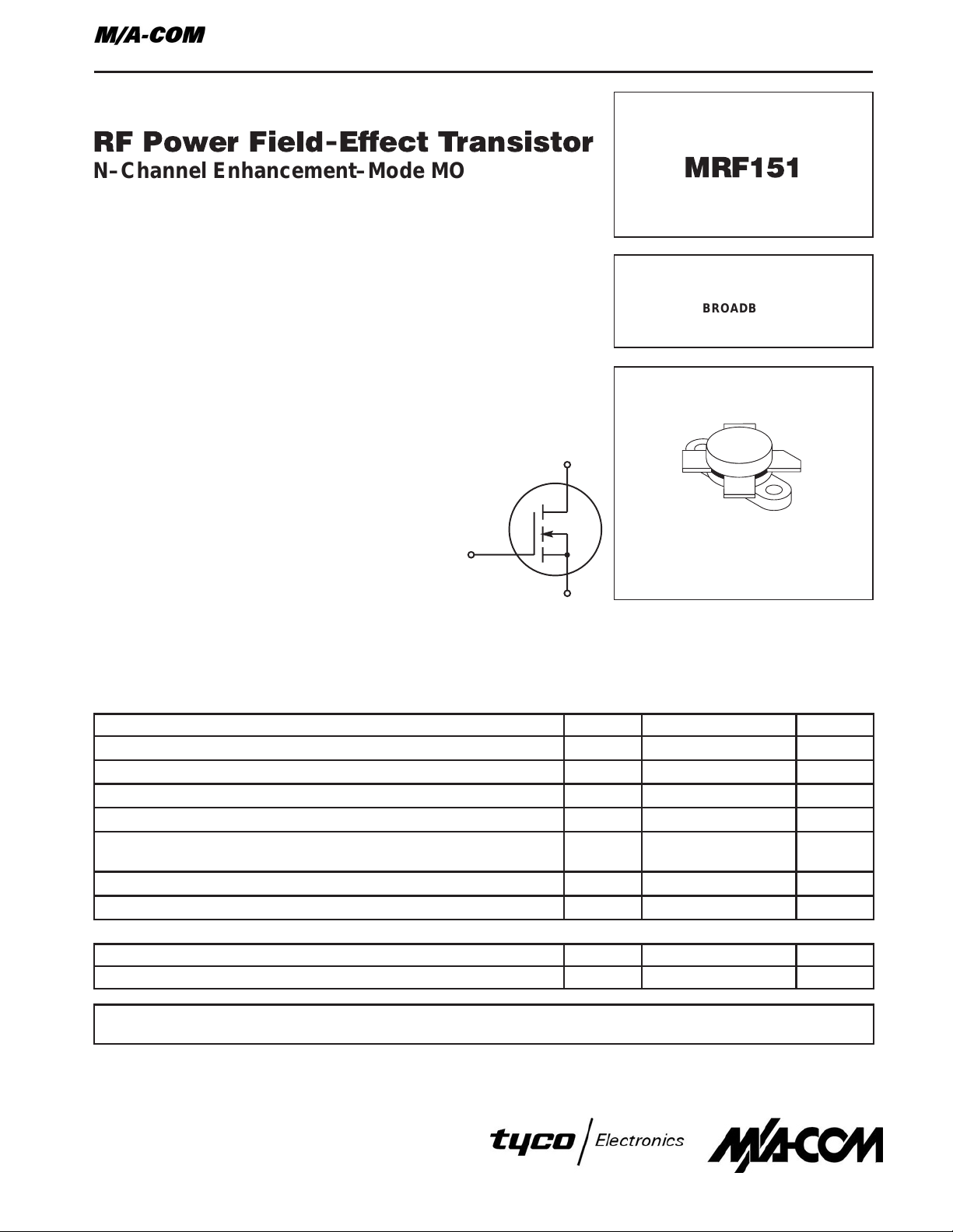
MRF151
150 W, 50 V, 175 MHz
N–CHANNEL
BROADBAND
RF POWER MOSFET
G
MAXIMUM RATINGS
Rating Symbol Value Unit
Drain–Source Voltage V
Drain–Gate Voltage V
Gate–Source Voltage V
Drain Current — Continuous I
Total Device Dissipation @ TC = 25°C
Derate above 25°C
Storage Temperature Range T
Operating Junction Temperature T
THERMAL CHARACTERISTICS
Characteristic Symbol Max Unit
Thermal Resistance, Junction to Case R
CASE 211–11, STYLE 2
S
DSS
DGO
GS
D
P
D
stg
J
θ
JC
125 Vdc
125 Vdc
±40 Vdc
16 Adc
300
1.71
–65 to +150 °C
200 °C
0.6 °C/W
Watts
W/°C
NOTE — CAUTION — MOS devices are susceptible to damage from electrostatic charge. Reasonable precautions in handling and
packaging MOS devices should be observed.
REV 9
1
Page 2
ELECTRICAL CHARACTERISTICS (T
= 25°C unless otherwise noted.)
C
Characteristic Symbol Min Typ Max Unit
OFF CHARACTERISTICS
Drain–Source Breakdown Voltage (VGS = 0, ID = 100 mA) V
Zero Gate Voltage Drain Current (VDS = 50 V, VGS = 0) I
Gate–Body Leakage Current (VGS = 20 V, VDS = 0) I
(BR)DSS
DSS
GSS
ON CHARACTERISTICS
Gate Threshold Voltage (VDS = 10 V, ID = 100 mA) V
Drain–Source On–Voltage (VGS = 10 V, ID = 10 A) V
Forward Transconductance (VDS = 10 V, ID = 5.0 A) g
GS(th)
DS(on)
fs
DYNAMIC CHARACTERISTICS
Input Capacitance (VDS = 50 V, VGS = 0, f = 1.0 MHz) C
Output Capacitance (VDS = 50 V, VGS = 0, f = 1.0 MHz) C
Reverse Transfer Capacitance (VDS = 50 V, VGS = 0, f = 1.0 MHz) C
iss
oss
rss
FUNCTIONAL TESTS
Common Source Amplifier Power Gain, f = 30; 30.001 MHz
(V
= 50 V, P
DD
= 150 W (PEP), IDQ = 250 mA) f = 175 MHz
out
Drain Efficiency
(V
= 50 V, P
DD
(Max) = 3.75 A)
I
D
= 150 W (PEP), f = 30; 30.001 MHz,
out
Intermodulation Distortion (1)
(V
= 50 V, P
DD
f2 = 30.001 MHz, I
= 150 W (PEP), f = 30 MHz,
out
= 250 mA)
DQ
Load Mismatch
(V
= 50 V, P
DD
= 250 mA, VSWR 30:1 at all Phase Angles)
I
DQ
= 150 W (PEP), f1 = 30; 30.001 MHz,
out
G
ps
η 40 45 — %
IMD
(d3)
IMD
(d11)
ψ
CLASS A PERFORMANCE
Intermodulation Distortion (1) and Power Gain
(V
= 50 V, P
DD
f2 = 30.001 MHz, I
= 50 W (PEP), f1 = 30 MHz,
out
= 3.0 A)
DQ
NOTE:
1. To MIL–STD–1311 Version A, Test Method 2204B, Two Tone, Reference Each Tone.
IMD
IMD
G
PS
(d3)
(d9–13)
125 — — Vdc
— — 5.0 mAdc
— — 1.0 µAdc
1.0 3.0 5.0 Vdc
1.0 3.0 5.0 Vdc
5.0 7.0 — mhos
— 350 — pF
— 220 — pF
— 15 — pF
18
—
22
13
—
dB
—
dB
—
—
–32
–60
–30
—
No Degradation in Output Power
—
—
—
23
–50
–75
—
dB
—
—
+
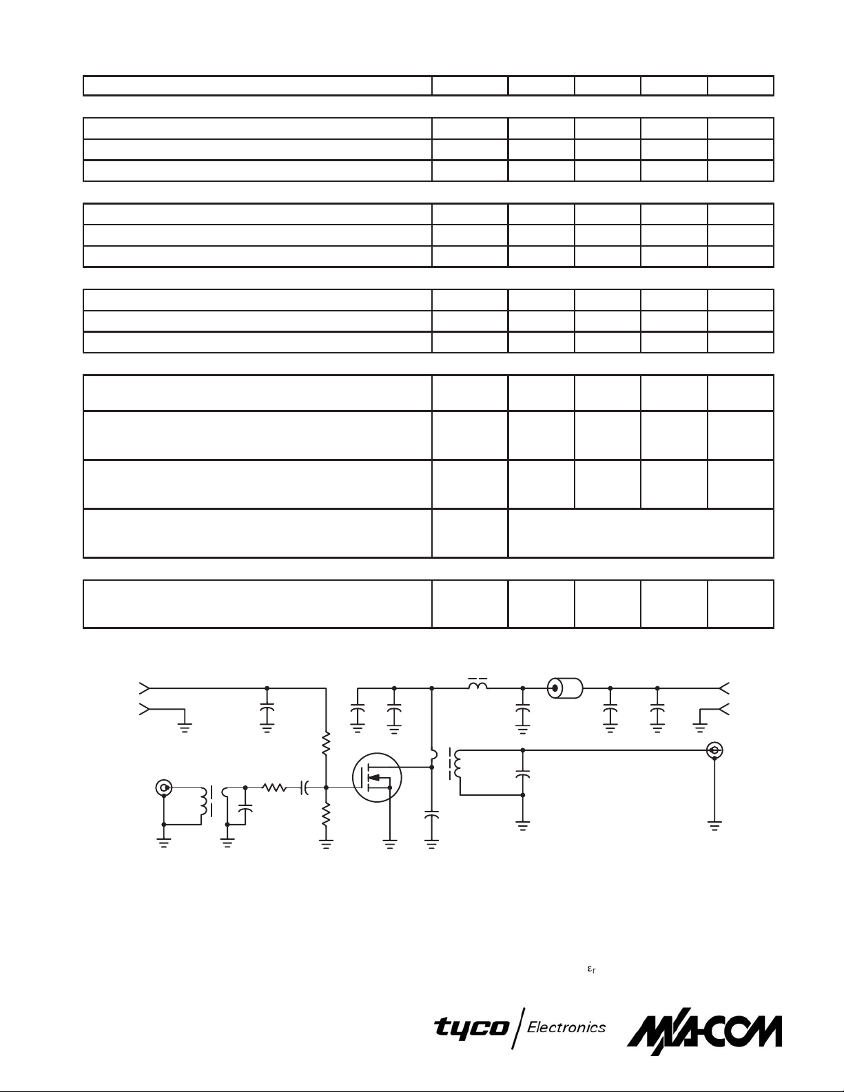
BIAS
0–12 V
–
RF
T1
C5
R3
INPUT
C1
C1 — 470 pF Dipped Mica
C2, C5, C6, C7, C8, C9 — 0.1 µF Ceramic Chip or
Monolythic with Short Leads
C3 — 200 pF Unencapsulated Mica or Dipped Mica
with Short Leads
C4 — 15 pF Unencapsulated Mica or Dipped Mica
with Short Leads
C10 — 10 µF/100 V Electrolytic
REV 9
2
C2
C6 C7 C8
R1
D.U.T.
R2
Figure 1. 30 MHz Test Circuit
L1
L2
+
C9 C10
–
T2
C4
C3
L1 — VK200/4B Ferrite Choke or Equivalent, 3.0 µH
L2 — Ferrite Bead(s), 2.0 µH
R1, R2 — 51 Ω/1.0 W Carbon
R3 — 3.3 Ω/1.0 W Carbon (or 2.0 x 6.8 Ω/1/2 W in Parallel)
T1 — 9:1 Broadband Transformer
T2 — 1:9 Broadband Transformer
Board Material — 0.062″ Fiberglass (G10),
1 oz. Copper Clad, 2 Sides,
e
= 5
r
+
50 V
–
RF
OUTPUT
Page 3
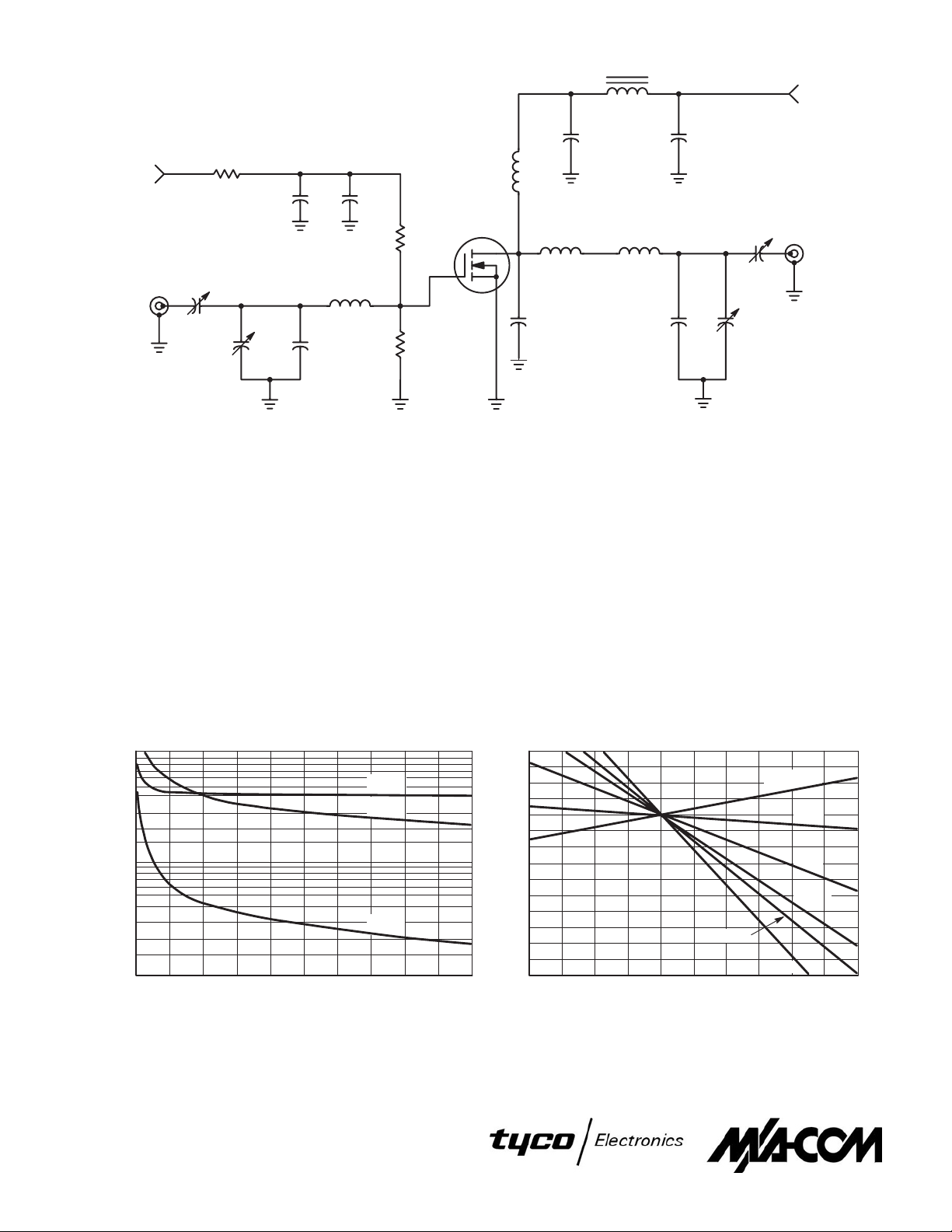
BIAS
0–12 V
R1
C4 C5
+
RFC2
+50 V
+
C10
L4
C11
RF INPUT
C1
C2 C3
C1, C2, C8 — Arco 463 or equivalent
C3 — 25 pF, Unelco
C4 — 0.1 µF, Ceramic
C5 — 1.0 µF, 15 WV Tantalum
C6 — 15 pF, Unelco J101
C7 — 25 pF, Unelco J101
C9 — Arco 262 or equivalent
C10 — 0.05 µF, Ceramic
C11 — 15 µF, 60 WV Electrolytic
D1 — 1N5347 Zener Diode
L1
R3
R2
D.U.T.
L3
C6
L1 — 3/4″, #18 AWG into Hairpin
L2 — Printed Line, 0.200″ x 0.500″
L3 — 1″, #16 AWG into Hairpin
L4 — 2 Turns, #16 AWG, 5/16 ID
RFC1 — 5.6 µH, Choke
RFC2 — VK200–4B
R1 — 150 Ω, 1.0 W Carbon
R2 — 10 kΩ, 1/2 W Carbon
R3 — 120 Ω, 1/2 W Carbon
Board Material — 0.062″ Fiberglass (G10),
1 oz. Copper Clad, 2 Sides, ε
Figure 2. 175 MHz T est Circuit
L2
C7
= 5.0
r
C9
RF OUTPUT
C8
TYPICAL CHARACTERISTICS
1000
C
500
200
100
50
C, CAPACITANCE (pF)
20
0
0 1020304050
VDS, DRAIN–SOURCE VOLTAGE (VOLTS)
Figure 3. Capacitance versus
Drain–Source Voltage
REV 9
3
iss
C
oss
C
rss
1.04
1.03
1.02
1.01
1
0.99
0.98
0.97
0.96
0.95
0.94
0.93
0.92
, DRAIN-SOURCE VOLTAGE (NORMALIZED)
0.91
GS
V
0.9
–25 0 25 50 75 100
TC, CASE TEMPERATURE (°C)
250 mA
1D = 5 A
4 A
2 A
1 A
100 mA
Figure 4. Gate–Source V oltage versus
Case T emperature
Page 4

TYPICAL CHARACTERISTICS
100
10
, DRAIN CURRENT (AMPS)
D
I
TC = 25°C
1
2 20 200
, DRAIN–TO–SOURCE VOLTAGE (VOLTS)
V
DS
Figure 5. DC Safe Operating Area Figure 6. Common Source Unity Gain Frequency
30
25
20
15
, POWER GAIN (dB)
PS
G
VDD = 50 V
10
I
= 250 mA
DQ
= 150 W
P
out
5
2 5 10 30 100 200
f, FREQUENCY (MHz)
Figure 7. Power Gain versus Frequency Figure 8. Output Power versus Input Power
2000
VDS = 30 V
VDS = 15 V
1000
, UNITY GAIN FREQUENCY (MHz)
T
f
0
0 4 8 12 16 20
2 6 10 14 18
ID, DRAIN CURRENT (AMPS)
versus Drain Current
300
200
100
0
0 5 10 15 20 25
300
200
, OUTPUT POWER (WATTS)
out
P
100
0
012345
VDD = 50 V
VDD = 50 V
P
40 V
, INPUT POWER (WA TTS)
in
f = 175 MHz
I
= 250 mA
DQ
f = 30 MHz
I
= 250 mA
DQ
REV 9
4
25
d
3
35
d
45
5
IDQ = 250 mA
55
V
= 50 V, f = 30 MHz, TONE SEPARATION = 1 kHz
DD
25
35
45
IMD, INTERMODULATION DISTORTION
55
20 60 100 140 180
0 40 80 120 160 200
d
3
d
5
, OUTPUT POWER (WA TTS PEP)
P
out
Figure 9. IMD versus P
IDQ = 500 mA
out
Page 5

150
f
f = 175 MHz
100
Z
in
30
MHz
30
40
50
60
70
80
90
100
110
120
130
140
150
160
170
180
190
200
210
220
230
240
15
150
30
f = 175 MHz
100
15
Zo = 10 Ω
VDD = 50 V
I
= 250 mA
DQ
= 150 W
P
out
ZOL* = Conjugate of the optimum load impedance
Z
* = into which the device output operates at a
OL
* = given output power, voltage and frequency.
Z
2
OL
7.5
7.5
4
ZOL*
4
2
NOTE: Gate Shunted by 25 Ohms.
Figure 10. Series Equivalent Impedance
T able 1. Common Source S–Parameters (VDS = 50 V, ID = 2 A)
S
11
|S11| φ |S21| φ |S12| φ |S22| φ
0.877
0.886
0.895
0.902
0.912
0.918
0.925
0.932
0.936
0.942
0.946
0.950
0.954
0.957
0.960
0.962
0.964
0.967
0.967
0.969
0.971
0.970
–174
–175
–175
–176
–176
–177
–177
–177
–178
–178
–179
–179
–180
–180
180
179
179
179
178
178
178
177
10.10
7.47
5.76
4.73
3.86
3.19
2.69
2.34
2.06
1.77
1.55
1.39
1.23
1.13
1.01
0.90
0.84
0.75
0.71
0.67
0.60
0.57
S
21
77
69
63
58
52
48
45
40
37
35
32
30
27
24
22
20
19
18
16
14
12
12
0.008
0.009
0.008
0.009
0.009
0.010
0.011
0.013
0.014
0.015
0.017
0.019
0.021
0.023
0.024
0.026
0.028
0.030
0.032
0.035
0.038
0.037
S
12
19
24
33
39
46
54
62
67
72
76
77
77
78
79
82
82
80
79
80
82
81
80
0.707
0.715
0.756
0.764
0.784
0.802
0.808
0.850
0.865
0.875
0.874
0.884
0.909
0.911
0.904
0.931
0.929
0.922
0.937
0.949
0.950
0.950
S
22
–169
–172
–171
–171
–172
–171
–171
–173
–175
–173
–172
–174
–175
–176
–177
–176
–178
–179
–180
180
179
179
REV 9
5
Page 6

T able 1. Common Source S–Parameters (VDS = 50 V, ID = 2 A) continued
f
MHz
250
260
270
280
290
300
310
320
330
340
350
360
370
380
390
400
410
420
430
440
450
460
470
480
490
500
S
11
S
21
S
12
S
22
|S11| φ |S21| φ |S12| φ |S22| φ
0.972
0.973
0.972
0.974
0.974
0.975
0.976
0.974
0.975
0.976
0.975
0.977
0.976
0.976
0.977
0.976
0.976
0.977
0.976
0.976
0.978
0.978
0.978
0.974
0.973
0.972
177
177
176
176
176
176
175
175
174
174
174
174
173
173
173
172
172
172
171
171
171
170
170
170
169
169
0.51
0.47
0.45
0.41
0.40
0.39
0.36
0.33
0.31
0.30
0.29
0.28
0.26
0.26
0.24
0.23
0.22
0.21
0.19
0.20
0.19
0.18
0.18
0.18
0.17
0.17
12
11
10
10
10
10
12
10
13
10
13
13
14
0.039
0.041
9
9
6
0.044
0.046
0.046
0.048
9
7
4
0.049
0.053
0.056
0.056
7
8
8
7
0.058
0.059
0.061
0.065
0.066
7
9
9
0.068
0.071
0.071
0.073
0.075
0.080
0.082
0.081
0.085
0.086
0.089
80
79
80
80
79
82
82
78
78
77
80
79
76
75
76
80
77
76
76
75
77
74
77
78
75
73
0.935
0.954
0.953
0.965
0.944
0.929
0.943
0.954
0.935
0.948
0.950
0.978
0.981
0.944
0.960
0.955
0.999
0.962
0.950
0.953
0.982
0.990
0.953
0.944
0.966
0.980
179
178
176
175
175
176
176
173
172
172
174
172
170
171
171
173
170
168
168
168
168
165
168
167
165
165
REV 9
6
Page 7

RF POWER MOSFET CONSIDERA TIONS
MOSFET CAPACITANCES
The physical structure of a MOSFET results in capacitors
between the terminals. The metal anode gate structure determines the capacitors from gate–to–drain (C
to–source (C
). The PN junction formed during the
gs
), and gate–
gd
fabrication of the MOSFET results in a junction capacitance
from drain–to–source (C
These capacitances are characterized as input (C
put (C
) and reverse transfer (C
oss
).
ds
) capacitances on data
rss
iss
), out-
sheets. The relationships between the inter–terminal capacitances and those given on data sheets are shown below. The
C
can be specified in two ways:
iss
1. Drain shorted to source and positive voltage at the gate.
2. Positive voltage of the drain in respect to source and zero
volts at the gate. In the latter case the numbers are lower.
However, neither method represents the actual operating conditions in RF applications.
DRAIN
C
ds
SOURCE
C
iss
C
oss
C
rss
= Cgd = C
= Cgd = C
= C
gd
gs
ds
GATE
C
gd
C
gs
LINEARITY AND GAIN CHARACTERISTICS
In addition to the typical IMD and power gain data presented, Figure 6 may give the designer additional information
on the capabilities of this device. The graph represents the
small signal unity current gain frequency at a given drain current level. This is equivalent to f
for bipolar transistors.
T
Since this test is performed at a fast sweep speed, heating of
the device does not occur. Thus, in normal use, the higher
temperatures may degrade these characteristics to some extent.
DRAIN CHARACTERISTICS
One figure of merit for a FET is its static resistance in the
full–on condition. This on–resistance, V
, occurs in the
DS(on)
linear region of the output characteristic and is specified under specific test conditions for gate–source voltage and drain
current. For MOSFETs, V
has a positive temperature
DS(on)
coefficient and constitutes an important design consideration
at high temperatures, because it contributes to the power
dissipation within the device.
GATE CHARACTERISTICS
The gate of the MOSFET is a polysilicon material, and is
electrically isolated from the source by a layer of oxide. The
input resistance is very high — on the order of 10
9
ohms —
resulting in a leakage current of a few nanoamperes.
Gate control is achieved by applying a positive voltage
slightly in excess of the gate–to–source threshold voltage,
V
.
GS(th)
Gate Voltage Rating — Never exceed the gate voltage
rating. Exceeding the rated V
can result in permanent
GS
damage to the oxide layer in the gate region.
Gate T ermination — The gate of this device is essentially
capacitor. Circuits that leave the gate open–circuited or float-
ing should be avoided. These conditions can result in turn–
on of the device due to voltage build–up on the input
capacitor due to leakage currents or pickup.
Gate Protection — This device does not have an internal
monolithic zener diode from gate–to–source. If gate protection is required, an external zener diode is recommended.
Using a resistor to keep the gate–to–source impedance
low also helps damp transients and serves another important
function. Voltage transients on the drain can be coupled to
the gate through the parasitic gate–drain capacitance. If the
gate–to–source impedance and the rate of voltage change
on the drain are both high, then the signal coupled to the gate
may be large enough to exceed the gate–threshold voltage
and turn the device on.
HANDLING CONSIDERATIONS
When shipping, the devices should be transported only in
antistatic bags or conductive foam. Upon removal from the
packaging, careful handling procedures should be adhered
to. Those handling the devices should wear grounding straps
and devices not in the antistatic packaging should be kept in
metal tote bins. MOSFETs should be handled by the case
and not by the leads, and when testing the device, all leads
should make good electrical contact before voltage is applied. As a final note, when placing the FET into the system it
is designed for, soldering should be done with a grounded
iron.
DESIGN CONSIDERATIONS
The MRF151 is an RF Power, MOS, N–channel enhancement mode field–effect transistor (FET) designed for HF and
VHF power amplifier applications.
M/A-COM Application Note AN211A, FETs in Theory and
Practice, is suggested reading for those not familiar with the
construction and characteristics of FETs.
The major advantages of RF power MOSFETs include
high gain, low noise, simple bias systems, relative immunity
from thermal runaway, and the ability to withstand severely
mismatched loads without suffering damage. Power output
can be varied over a wide range with a low power dc control
signal.
DC BIAS
The MRF151 is an enhancement mode FET and, therefore, does not conduct when drain voltage is applied. Drain
current flows when a positive voltage is applied to the gate.
RF power FETs require forward bias for optimum performance. The value of quiescent drain current (I
) is not criti-
DQ
cal for many applications. The MRF151 was characterized at
= 250 mA, each side, which is the suggested minimum
I
DQ
value of I
cation, I
. For special applications such as linear amplifi-
DQ
may have to be selected to optimize the critical
DQ
parameters.
The gate is a dc open circuit and draws no current. Therefore, the gate bias circuit may be just a simple resistive divider network. Some applications may require a more elaborate
bias system.
GAIN CONTROL
Power output of the MRF151 may be controlled from its
rated value down to zero (negative gain) by varying the dc
gate voltage. This feature facilitates the design of manual
gain control, AGC/ALC and modulation systems.
REV 9
7
Page 8

P ACKAGE DIMENSIONS
A
U
M
Q
1
4
32
M
R
B
D
K
J
H
C
E
SEATING
PLANE
NOTES:
1. DIMENSIONING AND TOLERANCING PER ANSI
Y14.5M, 1982.
2. CONTROLLING DIMENSION: INCH.
DIM MIN MAX MIN MAX
A 0.960 0.990 24.39 25.14
B 0.465 0.510 11.82 12.95
C 0.229 0.275 5.82 6.98
D 0.216 0.235 5.49 5.96
E 0.084 0.110 2.14 2.79
H 0.144 0.178 3.66 4.52
J 0.003 0.007 0.08 0.17
K 0.435 ––– 11.05 –––
M 45 NOM 45 NOM
__
Q 0.115 0.130 2.93 3.30
R 0.246 0.255 6.25 6.47
U 0.720 0.730 18.29 18.54
STYLE 2:
PIN 1. SOURCE
2. GATE
3. SOURCE
4. DRAIN
MILLIMETERSINCHES
CASE 211–11
ISSUE N
Specifications subject to change without notice.
n
North America: Tel. (800) 366-2266, Fax (800) 618-8883
n Asia/Pacific: Tel.+81-44-844-8296, Fax +81-44-844-8298
n
Europe: Tel. +44 (1344) 869 595, Fax+44 (1344) 300 020
Visit www.macom.com for additional data sheets and product information.
REV 9
8
 Loading...