

Page 1
SEMICONDUCTOR TECHNICAL DATA
The RF MOSFET Line
N–Channel Enhancement–Mode
Designed for power amplifier applications in industrial, commercial and
amateur radio equipment to 175 MHz.
• Superior High Order IMD
• Specified 50 Volts, 30 MHz Characteristics
Output Power = 30 Watts
Power Gain = 18 dB (Typ)
Efficiency = 40% (Typ)
• IMD
• IMD
• 100% Tested For Load Mismatch At All Phase Angles With
30:1 VSWR
• Lower Reverse Transfer Capacitance (3.0 pF Typical)
(30 W PEP) — –35 dB (Typ)
(d3)
(30 W PEP) — –60 dB (Typ)
(d1 1)
D
Order this document
by MRF148/D
30 W, to 175 MHz
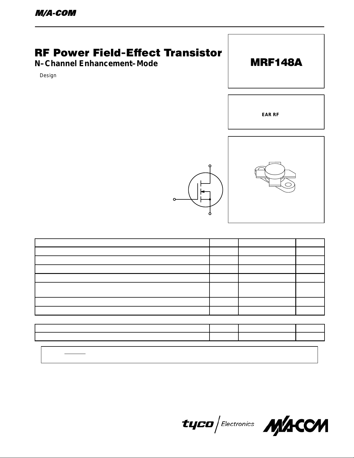
N–CHANNEL MOS
LINEAR RF POWER
FET
G
S
CASE 211–07, STYLE 2
MAXIMUM RATINGS
Rating Symbol Value Unit
Drain–Source Voltage V
Drain–Gate Voltage V
Gate–Source Voltage V
Drain Current — Continuous I
Total Device Dissipation @ TC = 25°C
Derate above 25°C
Storage Temperature Range T
Operating Junction Temperature T
DSS
DGO
GS
D
P
D
stg
J
120 Vdc
120 Vdc
±40 Vdc
6.0 Adc
115
0.66
–65 to +150 °C
200 °C
THERMAL CHARACTERISTICS
Characteristic Symbol Max Unit
Thermal Resistance, Junction to Case R
NOTE – CAUTION – MOS devices are susceptible to damage from electrostatic charge. Reasonable precautions in handling and
packaging MOS devices should be observed.
θJC
1.52 °C/W
Watts
W/°C
Replaces MRF148/D
1
Page 2
ELECTRICAL CHARACTERISTICS (T
Characteristic Symbol Min Typ Max Unit
= 25°C unless otherwise noted.)
C
OFF CHARACTERISTICS
Drain–Source Breakdown Voltage (VGS = 0, ID = 10 mA) V
Zero Gate Voltage Drain Current (VDS = 50 V, VGS = 0) I
Gate–Body Leakage Current (VGS = 20 V, VDS = 0) I
(BR)DSS
DSS
GSS
ON CHARACTERISTICS
Gate Threshold Voltage (VDS = 10 V, ID = 10 mA) V
Drain–Source On–Voltage (VGS = 10 V, ID = 2.5 A) V
Forward Transconductance (VDS = 10 V, ID = 2.5 A) g
GS(th)
DS(on)
DYNAMIC CHARACTERISTICS
Input Capacitance (VDS = 50 V, VGS = 0, f = 1.0 MHz) C
Output Capacitance (VDS = 50 V, VGS = 0, f = 1.0 MHz) C
Reverse Transfer Capacitance (VDS = 50 V, VGS = 0, f = 1.0 MHz) C
iss
oss
rss
FUNCTIONAL TESTS (SSB)
Common Source Amplifier Power Gain (30 MHz)
(VDD = 50 V, P
Drain Efficiency (30 W PEP)
(VDD = 50 V, f = 30 MHz, IDQ = 100 mA) (30 W CW)
Intermodulation Distortion
(VDD = 50 V, P
f = 30; 30.001 MHz, IDQ = 100 mA)
Load Mismatch
(VDD = 50 V, P
IDQ = 100 mA, VSWR 30:1 at all Phase Angles)
= 30 W (PEP), IDQ = 100 mA) (175 MHz)
out
= 30 W (PEP),
out
= 30 W (PEP), f = 30; 30.001 MHz,
out
G
η —
IMD
IMD
(d11)
ψ
CLASS A PERFORMANCE
Intermodulation Distortion (1) and Power Gain
(VDD = 50 V, P
f2 = 30.001 MHz, IDQ = 1.0 A)
NOTE:
1. To MIL–STD–1311 Version A, Test Method 2204B, Two Tone, Reference Each Tone.
= 10 W (PEP), f1 = 30 MHz,
out
IMD
G
PS
IMD
(d9–13)
fs
ps
(d3)
(d3)
125 — — Vdc
— — 1.0 mAdc
— — 100 nAdc
1.0 2.5 5.0 Vdc
1.0 3.0 5.0 Vdc
0.8 1.2 — mhos
— 62 — pF
— 35 — pF
— 3.0 — pF
—
—
—
—
—
No Degradation in Output Power
—
—
—
18
15
40
50
–35
–60
20
–50
–70
—
—
—
—
—
—
—
—
—
dB
%
dB
dB
BIAS
+
0–10 V
–
RF
INPUT
C1, C2, C3, C4, C5, C6 — 0.1 µF Ceramic Chip or Equivalent
C7 — 10 µF, 100 V Electrolytic
C8 — 100 pF Dipped Mica
L1 — VK200 20/4B Ferrite Choke or Equivalent (3.0 µH)
L2 — Ferrite Bead(s), 2.0 µH
Replaces MRF148/D
2
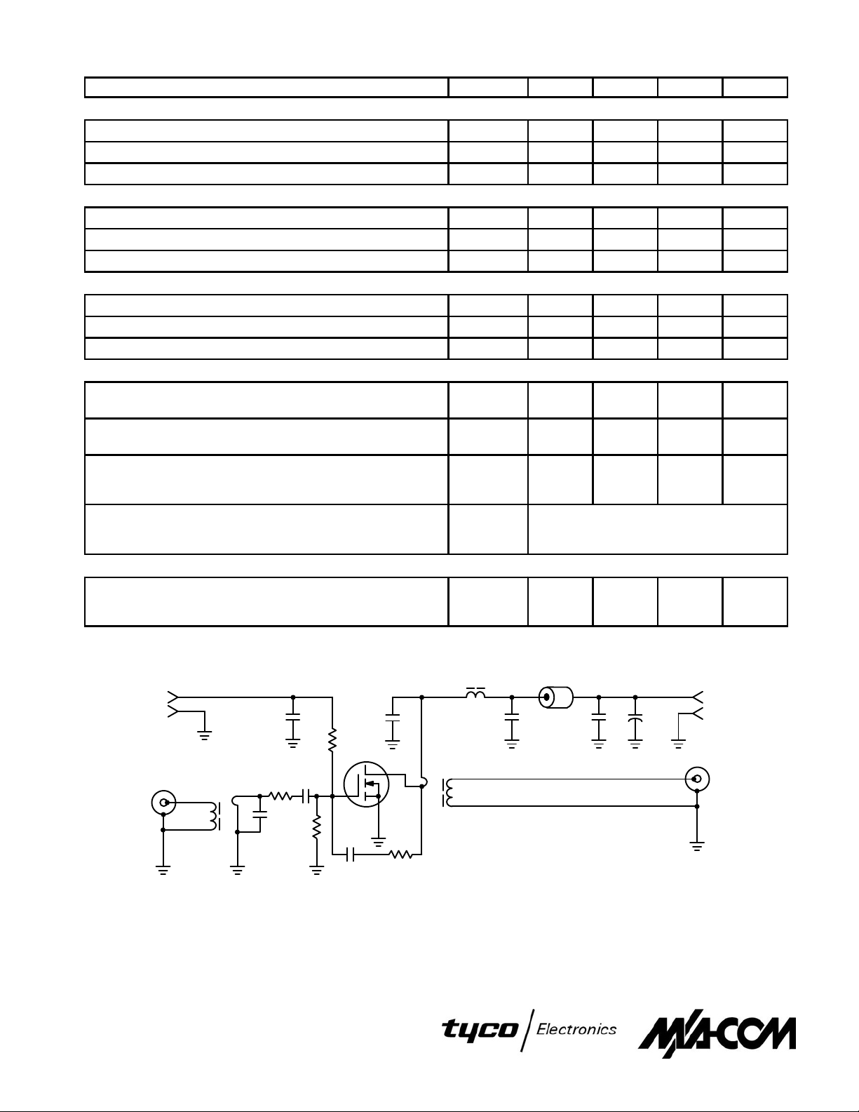
T1
L1
C1
C8
R3
R1
C2
R2
C4 C5 C6 C7
DUT
T2
C3
R4
Figure 1. 2.0 to 50 MHz Broadband Test Circuit
L2
+
R1, R2 — 200 Ω, 1/2 W Carbon
R3 — 4.7 Ω, 1/2 W Carbon
R4 — 470 Ω, 1.0 W Carbon
T1 — 4:1 Impedance Transformer
T2 — 1:2 Impedance Transformer
+
50 V
–
RF
OUTPUT
Page 3

25
60
20
15
10
POWER GAIN (dB)
5
0
2 5 10 20 20050 100
VDD = 50 V
IDQ = 100 mA
P
= 30 W (PEP)
out
f, FREQUENCY (MHz)
Figure 2. Power Gain versus Frequency Figure 3. Output Power versus Input Power
–30
–40
–50
–30
V
= 50 V, IDQ = 100 mA, TONE SEPARATION 1 kHz
DD
d
3
d
5
, OUTPUT POWER (WATTS)
out
P
2000
150 MHz30 MHz
1000
40
20
0
60
40
20
0
VDD = 50 V
40 V
IDQ = 100 mA
VDD = 50 V
40 V
IDQ = 100 mA
0 0.5 1 1.5 2 2.5
Pin, INPUT POWER (WATTS)
VDS = 30 V
VDS = 15 V
150 MHz30 MHz
d
–40
IMD, INTERMODULATION DISTORTION (dB)
–50
010203040
+ BIAS
0–6 V
RF INPUT
C1 — 91 pF Unelco Type MCM 01/010
C2, C4 — 0.1 µF Erie Red Cap
C3 — Allen Bradley 680 pF Feed Thru
C5 — 1.0 µF, 50 Vdc Electrolytic
C6 — 15 pF Unelco Type J101
C7 — 24 pF Unelco Type MCM 01/010
L1 — 2 Turns #18 AWG, 5/16″ ID
3
d
5
P
, OUTPUT POWER (WATTS PEP)
out
Figure 4. IMD versus P
R2
C3
C2
R1
C1
T1
out
L2
DUT
L2 — 4 Turns #18 AWG, 5/16″ ID
R1 — 1.0 Ohm, 1/4 W Carbon
R2 — 2000 Ohm, 1/4 W Carbon
RFC1 — VK200 21/4B
T1 — 4:1 Transformer, 1.75″ Subminiature
T1 — Coaxial Cable
, UNITY GAIN FREQUENCY (MHz)
T
f
0
01234
I
, DRAIN CURRENT (AMPS)
D
Figure 5. Common Source Unity Gain Frequency
versus Drain Current
C7
+ 50 Vdc
RF OUTPUT
Ω
50
12.5
Ω
C4
RFC1
L1
+
C5
C6
T1 — 4:1 Impedance Ratio
T1 — Transformer, Line
T1 — Impedance = 25 Ω
Replaces MRF148/D
3
Figure 6. 150 MHz T est Circuit
Page 4

2
1
, DRAIN CURRENT (AMPS)
DS
I
V
= 10 V
DS
gfs = 1.2 mho
10
7
5
3
2
1
0.7
0.5
, DRAIN CURRENT (AMPS)
D
0.3
I
0.2
TC = 25°C
0
0246810
13579
V
, GATE–SOURCE VOLTAGE (VOLTS)
GS
0.1
0.2 0.4
0.7 1 2 4 7 10 20 40 70 100 200
VDS, DRAIN–SOURCE VOLTAGE (VOL TS)
Figure 7. Gate Voltage versus Drain Current Figure 8. DC Safe Operating Area (SOA)
175
150
50
30
175
ZOL*
Replaces MRF148/D
4
f = 2.0 MHz
15
Z
in
7.0
4.0
f = 2.0 MHz
ZOL* = Conjugate of the optimum load impedance
ZOL* = into which the device output operates at a
ZOL* = given output power, voltage and frequency.
VDD = 50 V
IDQ = 100 mA
P
= 30 W PEP
out
Gate Shunted By 100
Figure 9. Impedance Coordinates — 50 Ohm
Characteristic Impedance
Ω
Page 5

RF POWER MOSFET CONSIDERA TIONS
MOSFET CAPACITANCES
The physical structure of a MOSFET results in capacitors
between the terminals. The metal oxide gate structure
determines the capacitors from gate–to–drain (Cgd), and
gate–to–source (Cgs). The PN junction formed during the
fabrication of the RF MOSFET results in a junction capacitance from drain–to–source (Cds).
These capacitances are characterized as input (C
output (C
) and reverse transfer (C
oss
) capacitances on data
rss
iss
sheets. The relationships between the inter–terminal capacitances and those given on data sheets are shown below. The
C
can be specified in two ways:
iss
1. Drain shorted to source and positive voltage at the gate.
2. Positive voltage of the drain in respect to source and zero
volts at the gate. In the latter case the numbers are lower.
However, neither method represents the actual operating conditions in RF applications.
DRAIN
C
ds
SOURCE
C
= Cgd + C
iss
C
oss
C
= C
rss
= Cgd + C
gd
gs
ds
GATE
C
gd
C
gs
LINEARITY AND GAIN CHARACTERISTICS
In addition to the typical IMD and power gain data
presented, Figure 5 may give the designer additional information on the capabilities of this device. The graph represents the
small signal unity current gain frequency at a given drain
current level. This is equivalent to fT for bipolar transistors.
Since this test is performed at a fast sweep speed, heating of
the device does not occur. Thus, in normal use, the higher
temperatures may degrade these characteristics to some
extent.
DRAIN CHARACTERISTICS
),
One figure of merit for a FET is its static resistance in the
full–on condition. This on–resistance, V
DS(on)
, occurs in the
linear region of the output characteristic and is specified under
specific test conditions for gate–source voltage and drain
current. For MOSFETs, V
has a positive temperature
DS(on)
coefficient and constitutes an important design consideration
at high temperatures, because it contributes to the power
dissipation within the device.
GATE CHARACTERISTICS
The gate of the RF MOSFET is a polysilicon material, and
is electrically isolated from the source by a layer of oxide. The
input resistance is very high — on the order of 109 ohms —
resulting in a leakage current of a few nanoamperes.
Gate control is achieved by applying a positive voltage
slightly in excess of the gate–to–source threshold voltage,
V
GS(th)
.
Gate Voltage Rating — Never exceed the gate voltage
rating. Exceeding the rated VGS can result in permanent
damage to the oxide layer in the gate region.
Gate Termination — The gates of these devices are
essentially capacitors. Circuits that leave the gate open–circuited or floating should be avoided. These conditions can
result in turn–on of the devices due to voltage build–up on the
input capacitor due to leakage currents or pickup.
Gate Protection — These devices do not have an internal
monolithic zener diode from gate–to–source. If gate protection
is required, an external zener diode is recommended.
Replaces MRF148/D
5
EQUIVALENT TRANSISTOR PARAMETER TERMINOLOGY
Collector Drain. . . . . . . . . . . . . . . . . . . . . . . . . . . . . . .
Emitter Source. . . . . . . . . . . . . . . . . . . . . . . . . . . . . . .
Base Gate. . . . . . . . . . . . . . . . . . . . . . . . . . . . . . .
R
CE(sat)
V
V
V
=
(BR)CES
V
CBO
I
C
I
CES
I
EBO
V
BE(on)
CE(sat)
C
ib
C
ob
h
fe
CE(sat)
I
C
. . . . . . . . . . . . . . . . . . . . . . . . . . . . . . .
. . . . . . . . . . . . . . . . . . . . . . . . . . . . . . .
. . . . . . . . . . . . . . . . . . . . . . . . . . . . . . .
. . . . . . . . . . . . . . . . . . . . . . . . . . . . . . .
. . . . . . . . . . . . . . . . . . . . . . . . . . . . . . .
. . . . . . . . . . . . . . . . . . . . . . . . . . . . . . .
. . . . . . . . . . . . . . . . . . . . . . . . . . . . . . .
. . . . . . . . . . . . . . . . . . . . . . . . . . . . . . .
. . . . . . . . . . . . . . . . . . . . . . . . . . . . . . .
. . . . . . . . . . . . . . . . . . . . . . . . . . . . . . .
. . . . . . . . . . . . . . . . . . . . . . . . . . . . . . . .
V
(BR)DSS
V
DGO
I
D
I
DSS
I
GSS
V
GS(th)
V
DS(on)
C
iss
C
oss
g
fs
r
DS(on)
V
=
DS(on)
I
D
Page 6

P ACKAGE DIMENSIONS
A
U
M
Q
1
4
32
S
K
M
B
R
D
J
H
C
E
SEATING
PLANE
NOTES:
1. DIMENSIONING AND TOLERANCING PER ANSI
Y14.5M, 1982.
2. CONTROLLING DIMENSION: INCH.
DIM MIN MAX MIN MAX
A 0.960 0.990 24.39 25.14
B 0.370 0.390 9.40 9.90
C 0.229 0.281 5.82 7.13
D 0.215 0.235 5.47 5.96
E 0.085 0.105 2.16 2.66
H 0.150 0.108 3.81 4.57
J 0.004 0.006 0.11 0.15
K 0.395 0.405 10.04 10.28
M 40 50 40 50
____
Q 0.113 0.130 2.88 3.30
R 0.245 0.255 6.23 6.47
S 0.790 0.810 20.07 20.57
U 0.720 0.730 18.29 18.54
STYLE 2:
PIN 1. SOURCE
2. GATE
3. SOURCE
4. DRAIN
MILLIMETERSINCHES
CASE 211–07
ISSUE N
Specifications subject to change without notice.
n
North America: Tel. (800) 366-2266, Fax (800) 618-8883
n Asia/Pacific: Tel.+81-44-844-8296, Fax +81-44-844-8298
n
Europe: Tel. +44 (1344) 869 595, Fax+44 (1344) 300 020
Visit www.macom.com for additional data sheets and product information.
Replaces MRF148/D
6
 Loading...