

Page 1

查询MR27V802D供应商
¡
Semiconductor
MR27V802D
524,288-Word x 16-Bit or 1,048,576-Word x 8-Bit One Time PROM
DESCRIPTION
The MR27V802D is a 8Mbit electrically Programmable Read-Only Memory whose configuration can
be electrically switched between 524,288 word x 16bit and 1,048,576 word x 8bit. The MR27V802D
operates on a single +3V-3.3V power supply and is TTL compatible. Since the MR27V802D
operates asynchronously , external clocks are not required , making this device easy-to-use. The
MR27V802D is suitable as large-capacity fixed memory for microcomputers and data terminals. It is
manufactured using a CMOS double silicon gate technology and is offered in 42-pin DIP, 44-pin
SOP or 44-pin TSOP packages.
FEATURES
• 524,288 word x 16bit / 1,048,576 word x 8bit electrically switchable configuration
• Single +3V-3.3V power supply
• Access time 100ns access time (Vcc=+3V)
80ns access time (Vcc=+3.3V)
• Input / Output TTL compatible
• Three-state output
• Packages
42-pin plastic DIP (DIP42-P-600-2.54) (Product name : MR27V802DRA)
44-pin plastic SOP (SOP44-P-600-1.27-K) (Product name : MR27V802DMA)
44-pin plastic TSOP (TSOP II 44-P-400-0.80-K) (Product name : MR27V802DTP)
1A
November 1999
1/11
Page 2
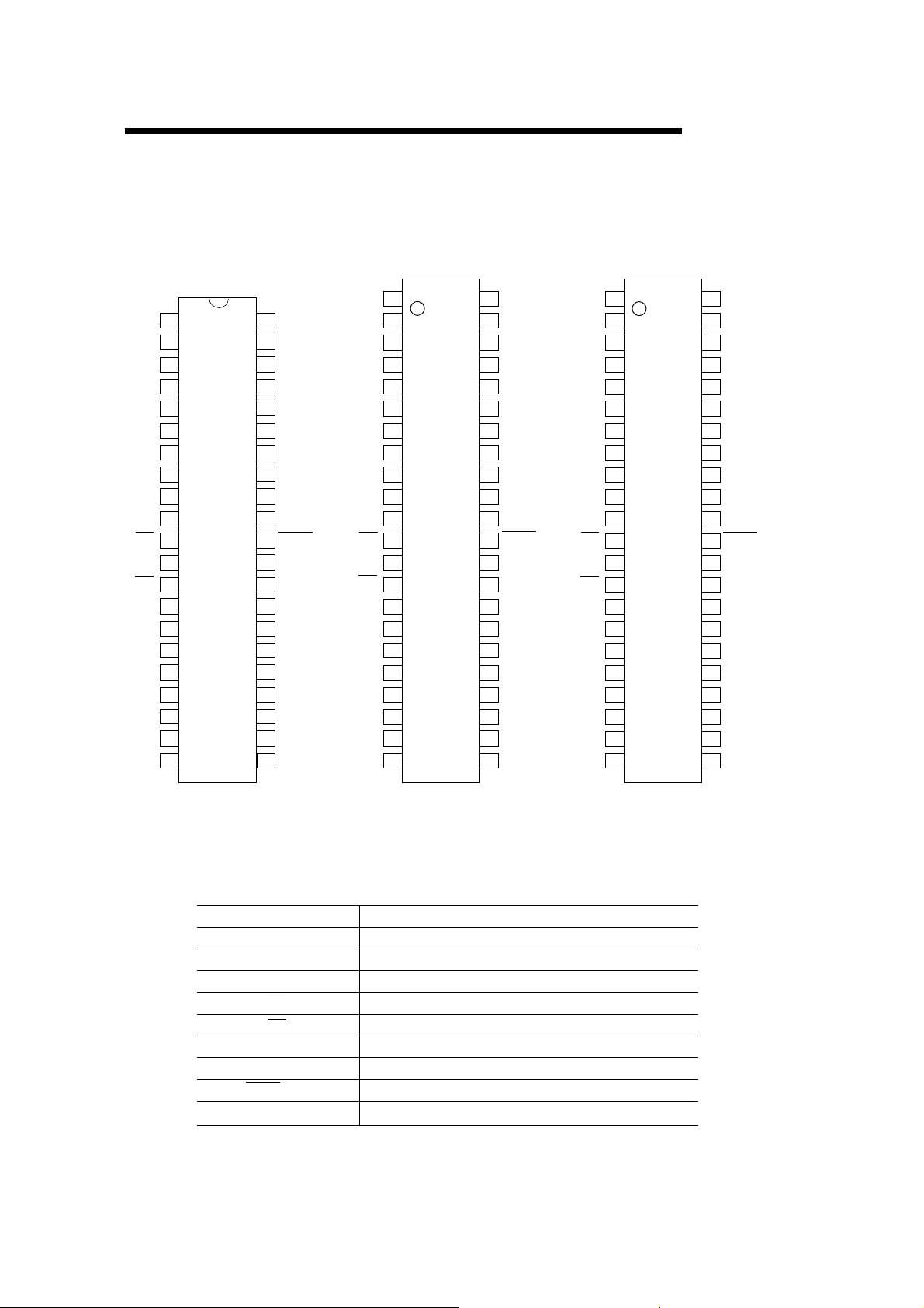
PIN CONFIGURATION (TOP VIEW)
MR27V802D
A18
A17
A7
A6
A5
A4
A3
A2
A1
A0
CE
V
SS
OE
D0
D8
D1
D9
D2
D10
D3
D11
10
11
12
13
14
15
16
17
18
19
20
21
NC
1
NC
1
2
3
4
5
6
7
8
9
42
A8
41
A9
40
A10
39
A11
38
A12
37
A13
36
A14
35
A15
34
A16
33
BYTE/Vpp
32
V
31
SS
D15/A-1
30
D7
29
D14
28
D6
27
D13
26
D5
25
D12
24
D4
23
V
22
CC
A18
A17
A7
A6
A5
A4
A3
A2
A1
A0
CE
V
SS
OE
D0
D8
D1
D9
D2
D10
D3
D11
2
3
4
5
6
7
8
9
10
11
12
13
14
15
16
17
18
19
20
21
NC
44
NC
43
A8
42
A9
41
A10
40
A11
39
A12
38
A13
37
A14
36
A15
35
A16
34
BYTE/Vpp
33
V
32
SS
D15/A-1
31
D7
30
D14
29
D6
28
D13
27
D5
26
D12
25
D4
24
V
2322
CC
NC
A18
A17
A7
A6
A5
A4
A3
A2
A1
A0
CE
V
SS
OE
D0
D8
D1
D9
D2
D10
D3
D11
10
11
12
13
14
15
16
17
18
19
20
21
NC
1
2
3
4
5
6
7
8
9
44
NC
43
A8
42
A9
41
A10
40
A11
39
A12
38
A13
37
A14
36
A15
35
A16
34
BYTE/Vpp
33
V
32
SS
D15/A-1
31
D7
30
D14
29
D6
28
D13
27
D5
26
D12
25
D4
24
V
2322
CC
42-pin DIP
PIN NAMES
FUNCTIONS
D15/A-1 Data output / Address input
A0-A18 Address input
D0-D14 Data output
CE
OE
V
CC
V
SS
BYTE/V
NC
PP
Chip enable
Output enable
Power supply voltage
GND
Mode switch / Program power supply voltage
Non connection
44-pin TSOP (II)44-pin SOP
2/11
Page 3
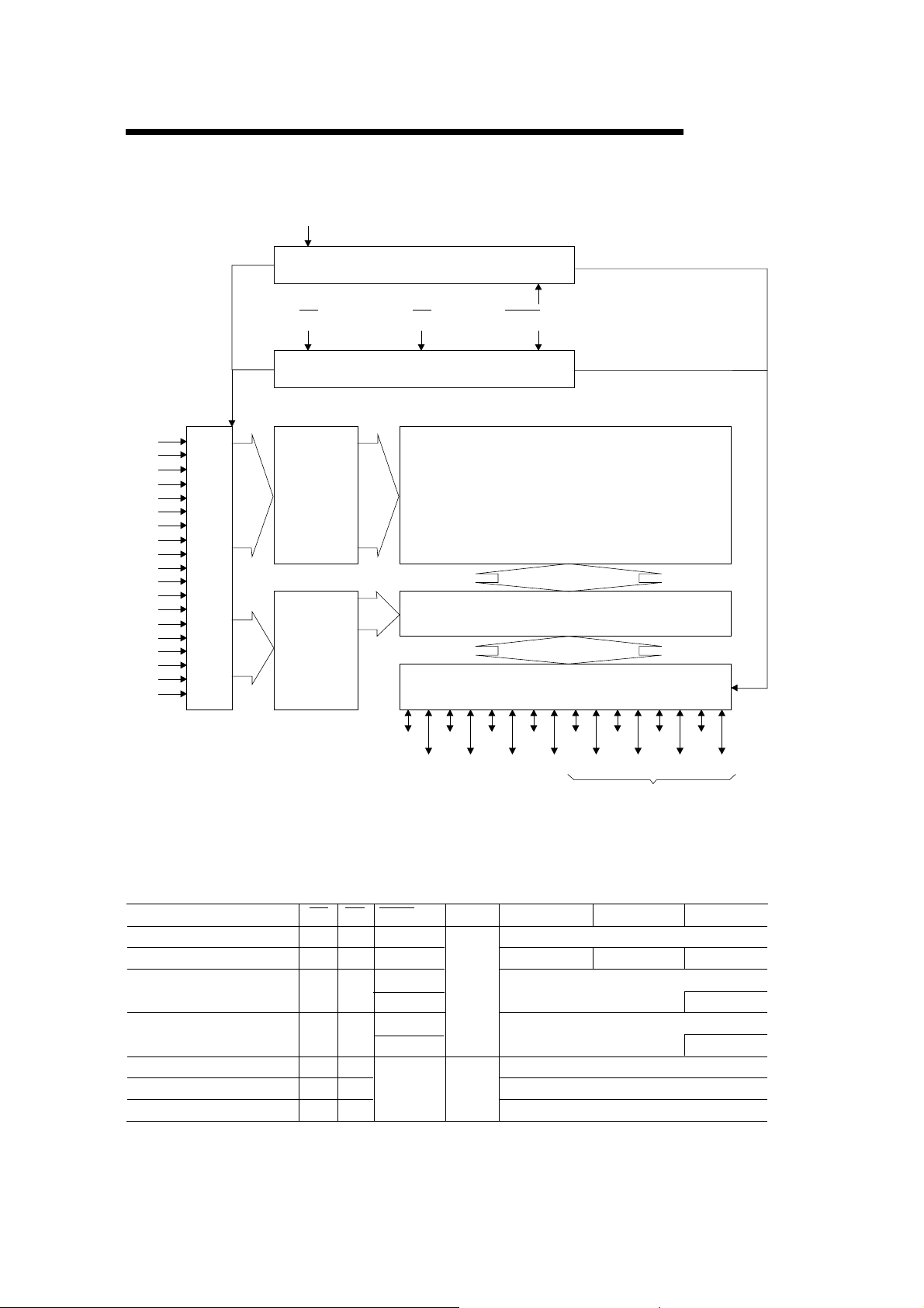
BLOCK DIAGRAM
MR27V802D
A-1
X8/X16 Switch
A0
A1
A2
A3
A4
A5
A6
A7
A8
A9
A10
A11
A12
A13
A14
A15
A16
A17
A18
Address Buffer
CE BYTE/V
OE
CE PGMOE
Memory Matrix
Row Decoder
524,288X16-Bit or 1,048,576X8-Bit
Multiplexer
Output Buffer
Column Decoder
D0
D1D2D3D4D5D6D7D8D9
PP
D10
D11
D12
D13
D14
D15
FUNCTION TABLE
MODE
READ (16-Bit)
READ (8-Bit)
OUTPUT DISABLE
STAND-BY
PROGRAM
PROGRAM INHIBIT
PROGRAM VERIFY
*: Don't Care
In 8-bit output mode, these pins are
three-stated and pin D15 functions
as the A-1 address pin.
CE OE
LL
L
L
H
L
H
*
BYTE/V
H
L
H
L
H
L
LH
H H Hi-Z
9.75V
HL
PP
V
CC
3.0V
to
3.3V
4.0V
D8 - D14D0 - D7
D
D
OUT
Hi-Z
Hi-Z
Hi-Z
D
D
D15/A-1
OUT
L/H
*
*
IN
OUT
3/11
Page 4
ABSOLUTE MAXIMUM RATINGS
MR27V802D
Parameter
Operating temperature under bias
Storage temperature
Input voltage
Output voltage
Power supply voltage
Program power supply voltage
Power dissipation per package
Symbol
Topr
T
stg
V
I
V
O
V
CC
V
PP
P
D
-
relative to V
-
SS
RECOMMENDED OPERATING CONDITIONS
Parameter Symbol
VCC power supply voltage
VPP power supply voltage
Input "H" level
Input "L" level
V
CC
V
PP
V
IH
V
IL
Voltage is relative to Vss
* : Vcc+1.5V (Max.) when pulse width of overshoot is less than 10nS.
** : -1.5V (Min.) when pulse width of undershoot is less than 10nS.
Condition
VCC=2.7V-3.6V
0 to 70
-55 to 125
+ 0.5
CC
(Ta=0 to 70°C)
Min. Max.
2.7
-0.5
Typ.
-
-
-
-
3.6
+0.5
V
CC
+0.5*2.2
V
CC
0.6-0.5**
UnitValueCondition
°C
°C
V-0.5 to V
V-0.5 to VCC +0.5
V-0.5 to 5
V-0.5 to 11.5
W1.0
Unit
V
V
V
V
4/11
Page 5

ELECTRICAL CHARACTERISTICS (Read operation)
DC Characteristics 1
Parameter
Input leakage current
Output leakage current
V
power supply current
CC
(Standby)
V
power supply current (Read)
CC
V
power supply current
PP
Input "H" level
Input "L" level
Output "H" level
Output "L" level
Voltage is relative to Vss
* : Vcc+1.5V (Max.) when pulse width of overshoot is less than 10nS.
** : -1.5V (Min.) when pulse width of undershoot is less than 10nS.
Symbol
I
LI
I
LO
I
CCSC
I
CCST
I
CCA
I
PP
V
IH
V
IL
V
OH
V
OL
CE=V
VI=0 to Vcc
VO=0 to Vcc
CE=V
CC
CE=V
IH
OE=V
IL,
V
IH
PP=VCC
tc=100ns
-
-
I
=-400uA
OH
I
=2.1mA
OL
MR27V802D
=3V±0.3V, Ta=0 to 70°C)
(V
CC
Min. Max.
2.2
2.4
Typ.
-
-
-
-
-
-
-
-
-
-
-
-
-
-
-
-
-
10
10
50
1
35
10
VCC+0.5*
0.6-0.5**
-
0.4
UnitCondition
µA
µA
µA
mA
mA
µA
V
V
V
V
DC Characteristics 2
Parameter
Input leakage current
Output leakage current
V
power supply current
CC
(Standby)
V
power supply current (Read)
CC
power supply current
V
PP
Input "H" level
Input "L" level
Output "H" level
Output "L" level
Symbol
I
LI
I
LO
I
CCSC
I
CCST
I
CCA
I
PP
V
IH
V
IL
V
OH
V
OL
CE=V
Condition
V
=0 to Vcc
I
=0 to Vcc
V
O
CE=V
CE=V
OE=V
IL,
V
PP=VCC
I
=-400uA
OH
=2.1mA
I
OL
CC
IH
-
-
IH
tc=80ns
Voltage is relative to Vss
* : Vcc+1.5V (Max.) when pulse width of overshoot is less than 10nS.
** : -1.5V (Min.) when pulse width of undershoot is less than 10nS.
=3.3V±0.3V, Ta=0 to 70°C)
(V
CC
Min. Max.
-
-
-
-
-
2.2 V
-0.5**
2.4
Typ.
-
-
-
-
-
-
-
-
-
-
-
10
1050
1
40
10
VCC+0.5*
0.6
-
0.4
Unit
µA
µA
µA
mA
mA
µA
V
V
V
5/11
Page 6

AC Characteristics 1
Parameter
Address cycle time
Address access time
CE access time
OE access time
Output disable time
Output hold time
Symbol
T
C
T
ACC
T
CE
T
OE
T
CHZ
T
OHZ
T
OH
Condition
CE=OE=V
OE=V
IL
CE=V
IL
OE=V
IL
CE=V
IL
CE=OE=V
MR27V802D
(V
=3V±0.3V, Ta=0 to 70°C)
CC
Min. Max.
100
IL
-
-
-
--
100
100
50
300
0
IL
0
25
-
Unit
ns
ns
ns
ns
ns
ns
ns
Measurement conditions
Input signal level
Input timing reference level
Output load
Output timing reference level
AC Characteristics 2
Parameter
Address cycle time
Address access time
CE access time
OE access time
Output disable time
Output hold time
Symbol
T
C
T
ACC
T
CE
T
OE
T
CHZ
T
OHZ
T
OH
Measurement conditions
Input signal level
Input timing reference level
Output load
Output timing reference level
0V/3V
0.8V/2.0V
100pF
0.8V/2.0V
Condition
-
CE=OE=V
OE=V
IL
CE=V
IL
OE=V
IL
CE=V
IL
CE=OE=V
0V/3V
0.8V/2.0V
100pF
0.8V/2.0V
(V
=3.3V±0.3V, Ta=0 to 70°C)
CC
Min. Max.
80
IL
-
-
-
0
-
80
80
40
30
250
IL
0
-
Unit
ns
ns
ns
ns
ns
ns
ns
Output
2.08V
800ohms
100pF
6/11
Page 7

TIMING CHART (READ CYCLE)
16-Bit Read Mode (BYTE=VIH)
A0 - A18
CE
OE
MR27V802D
t
C
t
t
CE
t
OE
OH
t
CHZ
D0 - D15
8-Bit Read Mode (BYTE=V
A-1 - A18
CE
OE
t
ACC
Valid Data
)
IL
t
C
t
CE
t
OE
t
ACC
t
OHZ
t
t
OH
t
CHZ
OHZ
Hi-ZHi-Z
D0 - D7
D8 - D14
Hi-Z
Valid Data
Hi-ZHi-Z
7/11
Page 8

ELECTRICAL CHARACTERISTICS (Programming operation)
DC Characteristics
MR27V802D
Parameter
Input leakage current
V
power supply current (Program)
PP
power supply current
V
CC
Input "H" level
Input "L" level
Output "H" level
Output "L" level
Program voltage
power supply voltage
V
CC
Voltage is relative to Vss
AC Characteristics
Parameter
Address set-up time
OE set-up time
Data set-up time
Address hold time
Data hold time
Output float delay from OE
voltage set-up time
V
PP
Program pulse width
Data valid from OE
Address hold from OE high
Symbol
I
LI
I
PP2
I
CC
V
IH
V
IL
V
OH
V
OL
V
PP
V
CC
Symbol
T
AS
T
OES
T
DS
T
AH
T
DH
T
OHZ
T
VS
T
PW
T
OE
T
AHO
Condition
V
I=VCC
CE=V
I
=2.1mA
OL
(Vcc=4.0V
Condition
+0.5V
IL
-
-
-
-
-
-
-
-
-
-
-
Min. Max.
-
-
-
3.0
-0.5
2.4
-
Typ.
-
-
--
-
-
-
-
9.75
3.9
±0.1V,V
pp
Min. Max.
100
2
100
2
100 ns
4.0
=9.75V±0.25V,Ta=25°C±5°C)
Typ.
-
-
--
-
0
2
-
10
-
0
--
--
(Ta=25°C
10
50
50
VCC+0.5
0.8
-
0.45
10.09.5
4.1
-
-
-
-
-
100
-
119
100
-
±5°C)
Unit
µA
mA
mA
V
V
VIOH=-400µA
V
V
V
Unit
ns
µs
ns
µs
ns-
µs
µs
ns
ns
Pin Check Function
Pin Check Function is to check contact between each device-pin and each socket-lead with EPROM
programmer.
Setting up address as the following condition call the preprogrammed codes on device outputs.
(Vcc=3.3V
A0
A2
A1
0
1
A3
0
1
A4
0
A5
1
A6
A8
A7
0
0
1
101010101VH* 1
±0.3V,CE=OE=V
A10
0
A11
A9
VH*
A12
,BYTE/Vpp=V
IL
A14
A13
A15
,Ta=25°C±5°C)
IH
A17
A16
A18
10101001
0
1010110
DATA
FF00
00FF
FFFFOther conditions
* :VH=8V
±0.25V
8/11
Page 9

Consecutive Programming Waveforms
A0 - A18
MR27V802D
t
AS
t
PW
CE
High
OE
t
DS
D0 - D15
t
VS
BYTE/V
PP
Consecutive Program Verify Waveforms
Din Din
t
AH
t
DH
A0 - A18
CE
OE
D0 - D15
BYTE/V
PP
t
ACC
High
t
AHO
t
OE
Dout
t
OHZ
Dout
9.75V
9/11
Page 10

Program and Program Verify Cycle Waveforms
A0 - A18
MR27V802D
CE
OE
D0 - D15
BYTE/V
PP
t
OHZ
t
AS
t
PW
t
OES
t
DS
t
DH
Din
t
OE
Dout
t
AHO
t
OHZ
9.75V
PIN Capacitance
Parameter
Input
BYTE/V
PP
Output
( ) : DIP only
Symbol
C
IN1
C
IN2
C
OUT
Condition
=0V
V
I
=0V
V
O
(VCC=3.3V, Ta=25°C, f=1MHz)
Min. Max.
-
--
--
Typ.
-
8 (10)
120
10 (12)
Unit
pF
10/11
Page 11

Programming / Verify Flow Chart
MR27V802D
Programming
Bad insertion
Increment Address
Start
NO
Pin Check
OK
Address = First location
VCC=4.0V
VPP=9.75V
Program 10µs
NO
Last Address ?
YES
Verify
Start
Pin Check
OK
Address = First location
VCC=3.0V
V
=3.0V
PP
Verify (One Byte)
V
=3.6V
CC
V
=3.6V
PP
Verify (One Byte)
NO
Bad insertion
NG
PASS
NG
Increment Address
Address = First location
X=0
Verify (One Byte)
PASS
NO
Last Address ?
YES
VCC=3.0V
V
=3.0V
PP
Verify (One Byte)
PASS
PASS
Device Passed Device Failed
NG
X=X+1
YES
X=2?
NO
Program 10µs
NG
Device Passed Device Failed
11/11
 Loading...