

Page 1

1 Semiconductor
MR27V3266D
2M x16 / 1M x32 Synchronous OTP ROM
DESCRIPTION
The MR27V3266D is a 32Mbit One Time Programmable Synchronous Read Only Memory whose configuration
can be electrically switched between 2,097,152 x16bit(word mode) and 1,048,576 x32bit(double word mode) by
the state of the /WORD pin. The MR27V3266D supports high speed synchronous read operations using a single
3.3V power supply.
FEATURES ON READ
- 3.3V power supply
- LVTTL compatible with multiplexed address
- Dual, electrically switchable configurations
2M x16(word mode) / 1M x32(double word mode)
- All inputs are sampled at the rising edge of the system clock
- High speed read operation
66MHz : CAS Latency=5
tRCDmin=2
Burst Length (4, 8)
Data scramble (sequential, interleave)
50MHz : CAS Latency=4, 5
tRCDmin=1
Burst Length (4, 8)
Data scramble (sequential, interleave)
- DQM for data out masking
- No Precharge operation is required. No Refresh operation is required.
- No power on sequence is required.
Mode register is automatically initialized to the default state after power on.
"Row Active" command to read data is applicable as the first command just after power on.
- Single Bank operation
- Package : TSOP II 86-P-400-0.50-K
FEATURES ON PROGRAMMING
- 9.75V programming Power supply
- Programming algorithm is compatible with conventional asynchronous 32M OTP.
MR27V3266D can be programmed with conventional EPROM programmers.
Synchronous Burst read or Static Programming Operation are selected by the state of STO pin.
High STO level enables full static programming. (Program, Program Verify, asynchronous Read)
Low STO level enables synchronous burst read.
Exclusive 86pin socket adapters are available from OKI to support programming requirements.
The socket adapter is used on a 48DIP socket on the programmer.
The socket adapter is designed with the STO pin connected to V
as conventional 32M OTP.
EPROM programmer must have the proper algorithm for 32M OTP.
*Device damage can occur if improper algorithm is used.
- High speed programming
10µs programming pulse per word allows high speed programming.
August , 1999
Revision 2.4
1
CC in order to program MR27V3266D
32M Synchronous OTP
Page 2
1 Semiconductor
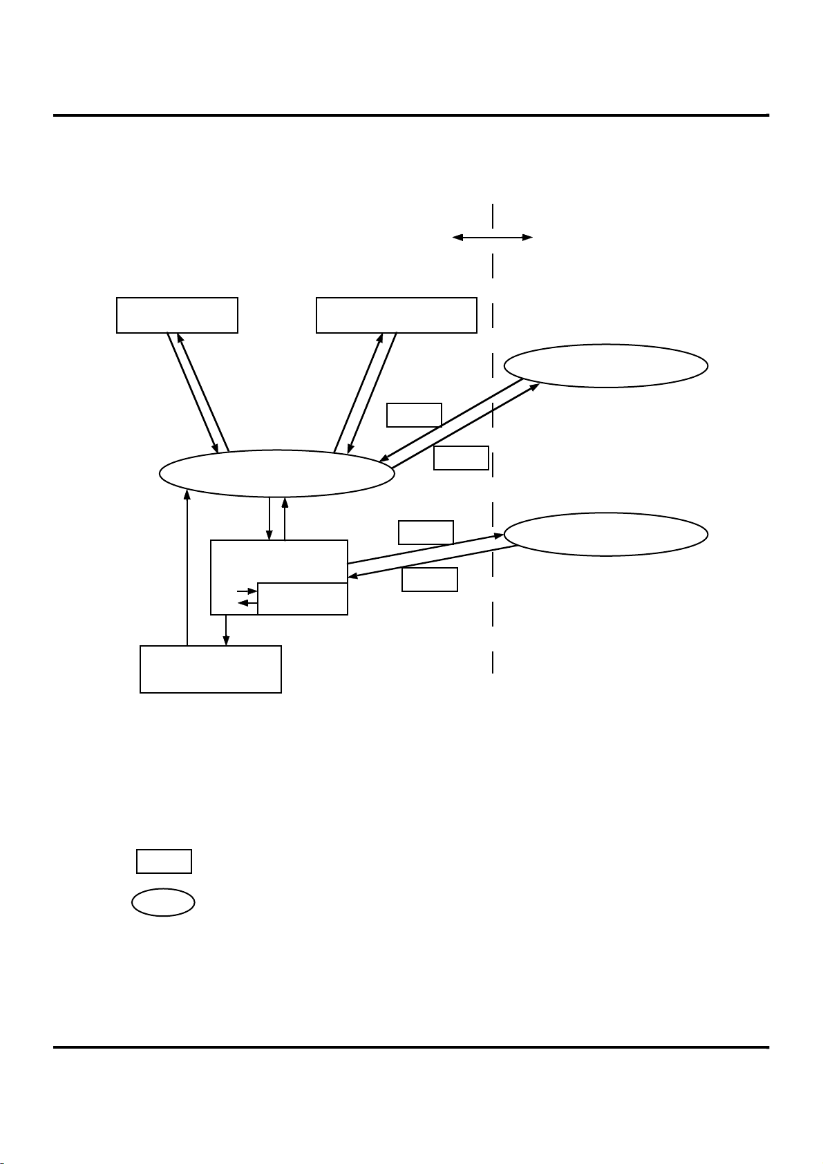
FUNCTION BLOCK DIAGRAM
A0
|
A12
Address Buffer
Latch
Row Address
Latch
Row Decoder
MR27V3266D
Memory Cell Array
1Mx32 or 2Mx16
Row Select
Column Select
Sence Amplifier
& Program Bias
CS
RAS
CAS
MR
WORD
Command
Controller
Mode
Register
CLK Buffer
CKE CLK
Column Address
Burst Sequence
Controller
Program Mode
Controller
OE
Column Decoder
STO DQ24-DQ31
CAP0-CAP7
Data Output
Latch
Data Outputs
Selector
Data Output/Input Buffer
& Data Output/Address Buffer
Data Input
Buffer
DQ0-DQ15
August , 1999
Revision 2.4
CE
AMPX
2
DQ16-DQ23
32M Synchronous OTP
Page 3
1 Semiconductor
PIN CONFIGURATION
Programming in Static Operation (STO is high)
MR27V3266D
TOP VIEW
Synchronous Read (STO is VSS or open)
VCC
DQ0
VCCQ
DC
DQ1
VSSQ
DC
DQ2
VCCQ
DC
DQ3
VSSQ
DC
DC
VCC
DC
NC
/CAS
/RAS
DC
/WORD
A12
A11
A10
A0
A1
A2
NC
VCC
NC
DQ4
VSSQ
DC
DQ5
VCCQ
DC
DQ6
VSSQ
DC
DQ7
VCCQ
DC
VCC
VCC
DQ0
VCCQ
DQ16
DQ1
VSSQ
DQ17
DQ2
VCCQ
DQ18
DQ3
VSSQ
DQ19
/MR
VCC
DQM
NC
/CAS
/RAS
/CS
/WORD
A12
A11
A10
A0
A1
A2
NC
VCC
NC
DQ4
VSSQ
DQ20
DQ5
VCCQ
DQ21
DQ6
VSSQ
DQ22
DQ7
VCCQ
DQ23
VCC
1
2
3
4
5
6
7
8
9
10
11
12
13
14
15
16
17
18
19
20
21
22
23
24
25
26
27
28
29
30
31
32
33
34
35
36
37
38
39
40
41
42
43
86PIN
TSOP II
86
85
84
83
82
81
80
79
78
77
76
75
74
73
72
71
70
69
68
67
66
65
64
63
62
61
60
59
58
57
56
55
54
53
52
51
50
49
48
47
46
45
44
VSS
DQ31
VSSQ
DQ15
DQ30
VCCQ
DQ14
DQ29
VSSQ
DQ13
DQ28
VCCQ
DQ12
NC
VSS
DC
DC
DC
CLK
CKE
A9
A8
A7
A6
A5
A4
A3
DC
VSS
DC
DQ27
VCCQ
DQ11
DQ26
VSSQ
DQ10
DQ25
VCCQ
DQ9
DQ24
VSSQ
DQ8
VSS
VSS
CAP0
VSSQ
DQ15
CAP1
VCCQ
DQ14
CAP2
VSSQ
DQ13
CAP3
VCCQ
DQ12
NC
VSS
VPP
/CE
/OE
DC
DC
A9
A8
A7
A6
A5
A4
A3
AMPX
VSS
STO
CAP4
VCCQ
DQ11
CAP5
VSSQ
DQ10
CAP6
VCCQ
DQ9
CAP7
VSSQ
DQ8
VSS
August , 1999
Revision 2.4
DC(Don't Care) : Logical input level is ignored, however the pin is connected to input buffer of OTP
32M Synchronous OTP
3
Page 4

1 Semiconductor
f
MR27V3266D
PIN FUNCTION FOR SYNCHRONOUS READ OPERATION ( STO pin is low level or open )
PIN NAME
STO
CLK
/CS
CKE
A0-A12
/RAS
/CAS
/MR
FUNCTION
Static Operation
System Clock
Chip Select
Clock Enable
Address
Row Address Strobe
Column Address Strobe
Mode Register Set
DESCRIPTION
Must be low for synchronous operation. Internal resistance
(around 10k ohms) pulls the input level down to V
this pin is open. High level STO enables programming
operation compatible with standard OTPs.
All inputs are sampled at the rising edge.
Enables command sampling by the CLK signal with a low level
on the /CS input.
Masks internal system clock to freeze the CLK operation o
subsequent CLK cycle. CKE must be enabled for command
sampling cycles. CLK is disabled for two types of operations.
1)Clock Suspend
2)Power down.
Row and column addresses are multiplexed on the same pins.
Row address:RA0-RA12
Column address:CA0-CA6(x32) / CA0-CA7(x16)
Functionality depends on the combination.
See the function table.
SS when
DQ0-DQ31
DQM
/WORD
VCC
SS
V
CCQ
V
SSQ
V
NC
DC
Data Output
Data Output Masking
x32/x16 Organization
Selection
Power Supply
Ground
Data Output Power Supply
Data Output Ground
No Connection
Don't Care
Data outputs are valid at the rising edge of CLK for read
cycles. Except for read cycles DQn is high-Z state.
Data outputs are masked after two cycles from when high
level DQM is applied.
The /WORD pin defines the organization of each read
command to be x16 (word mode) or x32 (double word mode).
High=x32
Low=x16
3.3V Power supply
3.3V Power supply to DQ0-DQ31
Logical input level is ignored.
August , 1999
Revision 2.4
32M Synchronous OTP
4
Page 5

1 Semiconductor
PIN FUNCTION FOR PROGRAMMING OPERATION ( STO pin is high level )
MR27V3266D
PIN NAME
STO
AMPX
A0-A12
/RAS
/CAS
DQ0-DQ15
FUNCTION
Static Operation
Address Multiplex
Address
Row address strobe
Column address strobe
Data Input/Output
DESCRIPTION
Must be set high for programming operation. Internal
resistance (around 10k ohms) pulls the input level down to
V
SS for open state condition to be low level for synchronous
read operation.
When AMPX is low, the addresses are not multiplexed and all
address bits must be supplied to A0-A12(Row Address) and
CAP0-CAP7(Column Address) simultaneously.
This pin should be set low on programming operation.
When AMPX is low, A0-A12 is row address input.
When AMPX is low, input is not used.
When AMPX is low, input is not used.
Input of data for programming and output for program verify
and read data.
/WORD
CAP0-CAP7
/OE
/CE
V
CC/VSS
VCCQ/VSSQ Data Output Power/Ground
VPP
x32/x16 organization Selection
Address Input
Output Enable
Chip Enable
Power Supply/Ground
Program Power Supply
The /WORD pin defines the organization to be x16(word
mode) or x32(double word mode).
High= x32
Low = x16
Must be set low for programming operation.
When /WORD is low, High-Z state on CAP0-CAP7 is held to
be input pins.
When AMPX is low, CAP0 - CAP7 is column address input.
Control signal input for programming.
/OE of conventional OTP.
Control signal input for programming.
Function for programming is associated with conventional
OTP.
Power and ground for the input buffers and the core logic.
Power and ground for output.
High voltage program power is supplied through V
When V
between V
V
PP mode. To keep stable static read operation VPP pin must
be kept lower than V
PP is higher than a predetermined voltage level
CC+0.5V and VCC+2V, pin function alters to high
CC+0.5V.
PP pin.
The functionality of loose device programming must be studied with the specification of socket adapter that will be
supplied by OKI. MR27V3266D on the socket adapter is the same programming functionality as conventional OTP.
August , 1999
Revision 2.4
5
32M Synchronous OTP
Page 6
1 Semiconductor
FUNCTION TABLE FOR SYNCHRONOUS READ
MR27V3266D
COMMAND NAME
Mode Register Set
Row Active
Read Word
(x16)
Read Double Word
(x32)
Burst Stop
Precharge
Clock Suspend
(on Read)
Power Down
(on Active
Standby)
Read Output
Mask Output
No Operation
( H=Logical high, L=Logical low, X=Don't Care, L of STO includes pin open due to internal pull down resistor )
Note
1. Refer to "Mode register Field Table" for Address Codes, and Mode Transition Chart for operational state.
After power on any command can be sampled at any cycle in Active Standby state.
After "Mode register Set" command is sampled, no new command can be accepted for 3 CLK cycles.
The /CS input must be kept high for the 3 CLK cycles to prevent unexpected sampling of a command.
2. The "Row Active" command is effective till new "Row Active" command is implemented.
3. The /WORD input is sampled simultaneously with "Read" command to select data width.
A Double Word Burst(x32 ) or a Word Burst(x16) is selected by the /WORD input for each "Read" command.
On condition of constant voltage level on /Word pin, organization is fixed to either x16 or x32.
"Read" command ends it's implementation by itself at the finishing cycle of the burst read.
4. Since OTP technology uses static sense amplifiers, the "Precharge" command is not required however,
due to customer request for the similarity of logical input code with SDRAM command, the name of
"Precharge" is adopted. Function of "Precharge" command and "Burst Stop" command is only to stop the burst
read cycles delayed by CAS Latency.
5. Sampled low level CKE disables CLK buffer to suspend internal clock signals at the next rising edge of CLK.
Sampled high level CKE enables internal clock at the next rising edge of CLK.
Low level CKE sampled in the period from the simultaneous cycle with a "Read" command till the end of the
burst read cycle is distinguished with internal command controller from the low level CKE sampled in Active
Standby state not to stop data sensing and burst read operation those consume power.
6. Low level CKE sampled in Active Standby state cuts power dissipation to be in Power Down state.
High level CKE sampled in Power Down state enables internal CKE to be in Active Standby state with
preserved row address.
FUNCTION
Mode Register Set
Row Address Latch
Column Address Latch
Trigger Burst Read
Column Address Latch
Trigger Burst Read
Burst Stop
Burst Stop
Entry
Exit
Entry
Exit
Output Enable
High-Z Output
Write on SDRAM
Self Refresh on SDRAM
Illegal on SDRAM
( CKEn expresses the logical level at the simultaneous cycle with a command. )
CKE
H
H
H
H
H
H
H
H
H
H
H
H
H
H
H
n-1 NotesSTO/WORDAdd.DQM/MR/CAS/RAS/CSCKEn
L
L
X
X
X
X
X
X
H
H
X
X
X
H
X
X
L
H
X
X
X
X
X
X
X
L
HH
L
H
L
L
L
X
X
X
X
X
X
LL
H
L
H
L
X
LL
L
L
H
L
H
L
H
L
LH
LL
L
X
X
L
X
X
X
H
L
X
X
X
X
X
X
H
L
L
L
L
L
L
X
H
HHH
L
X
X
X
X
X
X
X
X
X
X
H
X
X
X
X
X
Code
RA
CA
CA
L
X
X
X
X
X
X
X
X
X
X
X
X
X
X
X
L
HH
X
X
X
X
X
X
X
X
X
X
X
X
X
1
L
2
L
3
L
3
L
4
L
4
L
5
L
5
L
6
L
6
L
L
L
L
L
L
L
L
August , 1999
Revision 2.4
32M Synchronous OTP
6
Page 7
1 Semiconductor
MODE REGISTER FIELD TABLE
Address A5 A0A1A2A3A4
CAS Latency Burst Type Burst LengthFunction
MR27V3266D
A3A4A5
0
0
0
0
0
0
0
1
1
1
1
Note
A7 and A8 must be low during Mode Register Set cycle.
During power on, mode register is initialized to the default state when V
The default state of Mode Register is below. (less than 3.0V)
CAS Latency=5
Burst Type=Sequential
Burst length=4
1
1
000
0
1
1
1
0
1
1
1
Length
Reserved
Reserved
Reserved
4
5
Reserved
Reserved
Reserved
BURST SEQUENCE ( BURST LENGTH = 4 )
Initial address
A1 A0
0
0
Sequential Interleave
0
1
2
0
3
1
Type
A2
Sequential
0
Interleave
1
CC reaches a specific voltage.
2
3
A0A1
00
0
1
0
1
1
1
Length
Reserved
4
8
Reserved
0
1
1
0
11
1
2
2
3
0
3
0
3
0
1
1
2
0
1
2
3
2
3
BURST SEQUENCE ( BURST LENGTH = 8 )
Initial address
0
0
0
0
1
1
1
1
August , 1999
Revision 2.4
A0A1A2
0
0
1
0
0
1
0
0
1
1
1
2
0
2
3
11
3
4
0
4
5
1
5
6
0
6
7
11
7
Sequential
2
34
3
4
5
6
71
001
1
5
4
6
5
7
6
0
7
0
2
2
3
2
3
0
1
0
1
Interleave
5
6
7
0
1
2
34
6
7
0
1
7
0
1
2
0
1
2
3
1
2
3
4
2
3
3
4
4
5
5
4
5
6
6
7
3
2
3
001
2
5
4
7
6
0
1
6
7
6
71
4
5
5
4
5
6
7
0
2
312
5
6
7
6
7
4
4
7
6
0
3
5
5
4
3
2
3
2
0
1
0
1
32M Synchronous OTP
7
Page 8
1 Semiconductor
ADDRESSING MAP
(1) /WORD = "H" : x32 Organization
MR27V3266D
Pin Name
Row Address
Column Address
(2) /WORD = "L" : x16 Organization
Pin Name
Row Address
Column Address
(3) Programming
Address displayed on
programmer : x16
Device Address : x16
STO = "H", AMPX = "L"
Address ( STO = "L" )
/WORD = "L" : x16
Address ( STO = "L" )
/WORD = "H" : x32
Address displayed on
programmer : x16
Device Address : x16
STO = "H", AMPX = "L"
Note1
Note2 Note3
CA1
Ad13 Ad14
A5 A6
A5 A6A2 A3 A4A0 A1 A7 A8 A9 A10 A11 A12
RA5 RA6RA2 RA3 RA4RA0 RA1 RA7 RA8 RA9 RA10 RA11 RA12
CA5 CA6CA2 CA3 CA4CA0CA1 XXXXXX
A5 A6A2 A3 A4A0 A1 A7 A8 A9 A10 A11 A12
RA5 RA6RA2 RA3 RA4RA0 RA1 RA7 RA8 RA9 RA10 RA11 RA12
CA5 CA6CA2 CA3 CA4CA0 CA1 CA7 X X X X X
Ad5 Ad6Ad2 Ad3 Ad4Ad0 Ad1 Ad7 Ad8 Ad9 Ad10 Ad11 Ad12
CAP5 CAP6CAP2 CAP3 CAP4CAP0 CAP1 CAP7 A2 A3 A4A0 A1
CA3 CA4CA0
CA5 CA6
CA5 CA6
CA7
CA3 CA4CA0
CA2
Note4
Note5
CA2
CA1
Ad15 Ad16 Ad17 Ad18 Ad19 Ad20
A7 A8 A9 A10 A11 A12
( X = Don't Care )
( X = Don't Care )
RA2 RA3 RA4RA0 RA1
RA2 RA3 RA4RA0 RA1
Address ( STO = "L" )
/WORD = "L" : x16
Address ( STO = "L" )
/WORD = "H" : x32
User of MR27V3266D is recommended to study the relation between "Address displayed on programmer" and
"Address(STO="L")" ignoring "Device Address:x16, STO="H"".
Order of data on Synchronous Read operation(STO="L") is checked on this table.
"Device Address:x16, STO="H"" will be utilized to design socket adapter on programmer or to check boards
designed to mount blank OTP and program OTP on board.
OKI will supply socket adapter to program MR27V3266D as conventional x16 standard OTP. The users and the
venders of programmer who use the socket adapter can ignore "Device Address:x16, STO="H"".
Note
1. A0 in programmer distinguishes upper word(x16) or lower word(x16) of Double word(x32).
On word(x16) organization the address of device corresponds to the address of programmer.
On double word(x32) organization the address numeral code of device is half of that in programmer, and
output on DQ0-DQ15 is lower word(A0="0") and output on DQ16-DQ31 is upper word(A0="1").
2. CA1 is MSB of burst read on condition of /WORD="L" and BL=4
3. CA2 is MSB of burst read on condition of /WORD="L" and BL=8
4. CA1 is MSB of burst read on condition of /WORD="H" and BL=4
5. CA2 is MSB of burst read on condition of /WORD="H" and BL=8
RA5 RA6 RA7 RA8 RA9 RA10 RA11 RA12
RA5 RA6 RA7 RA8 RA9 RA10 RA11 RA12
August , 1999
Revision 2.4
32M Synchronous OTP
8
Page 9

1 Semiconductor
MR27V3266D
READ OPERATIONS
CLOCK ( CLK )
The clock input enables MR27V3266D to sample all the inputs, control internal circuitry, and turn on output drivers. All
timings are referred to the rising edge of the clock. All inputs with high level CKE and low level /CS should be valid at
the rising edge of CLK for proper functionality.
CLOCK ENABLE ( CKE )
The clock enable(CKE) turns on or switches off the admission of the clock input into the internal clock signal lines. All
internal circuits are controlled by the internal clock signal to implement every command. High level CKE sampled at
CKEn-1 clock cycle enables the admission of the rising edge of clock input into internal clock line at CKEn cycle. Low
level CKE sampled at CKEn-1 cycle suspends the rising edge of CLK at CKEn cycle. The suspension of internal clock
signal in all state ignores new input except CKE, and holds internal state and output state. Low level CKE in Active
Standby state, defined as Power Down state, cuts power dissipation. In Power Down state the contents of mode
register and Row Address are preserved. After recovering high level CKE to exit from Power Down state,
MR27V3266D is in Active Standby state. Low level CKE just after the sampling of "Read" command till the completion
of burst read, defined as Clock Suspend, makes read operation go on with power dissipation. Any command operation
does not interrupted by arbitrary low level CKE. Sampling command with low level CKE preceded with high level CKE is
illegal.
POWER ON
Apply power and start clock considering following issues.
1. During power on Mode Register is initialized into default state.
(default state: CAS latency=5, Burst Type=Sequential, Burst length=4)
2. After power on MR27V3266D is in Active Standby state and ready for "Mode Register set" command or
"Row Active" command. MR27V3266D requires neither command nor waiting time as power on sequence after
starting CLK input in order to start "Row Active" command to read data.
3. It is recommended in order to utilize default state of Mode Register that /MR and CKE inputs are maintained
to be pulled up during power on till the implementation of the first "Row Active" command.
After above power on "Row Active" command and "Read" command can be started immediately on default
Mode Register state.
4. It is recommended that DQM input is maintained to be pulled up to prevent unexpected operation of output
buffers.
ORGANIZATION CONTROL
Organization of data output(DQ0-DQ31) depends on the logical level on /WORD at the input timing of every "Read"
command. High level sampling of /WORD derives double word mode(x32) output and low level sampling of /WORD
derives word mode(x16) output. Constant /WORD level input brings consistent organization.
MODE REGISTER
Mode register stores the operating mode of MR27V3266D. Operating modes are consisted with CAS latency, Burst
Type, and Burst Length. Registration of RAS latency is not required, because RAS to CAS delay(tRCD) is requested
independently of system clock. When the contents of Mode register are required to be changed for the next
operation, "Mode Register Set" command can be sampled at any cycle in Active Standby state. After "Mode Register
Set" command is sampled, /CS must be fixed to logical high level to prevent sampling of new command input during
succeeding three clock cycles.
Refer to Mode Register Field Table for the relation between Operation modes and input pin assignment.
August , 1999
Revision 2.4
32M Synchronous OTP
9
Page 10

1 Semiconductor
MR27V3266D
READ OPERATIONS
CAS LATENCY
After sampling "Read" command MR27V3266D starts actual data read operation with sense amplifiers, and transmits
the data from sense amplifiers to data out buffers to start burst read. This flow of sequential functionality takes time
as clock cycles defined as CAS latency(CL). CAS latency is set in Mode Register as either four cycles or five cycles.
In this sequence(from sampling "Read" command to start of driving data bus) sense amplifiers consume maximum
current flow. The detailed sequence is below.
1. Fix column address of memory matrix driver. Row address is already fixed with "Row Active" command.
(at 1st cycle)
2. Read data of selected memory cells with sense amplifiers.
3. Deliver data detected with sense amplifiers to the register for data output latch.
4. Couple selectively the section of the register storing each (double)word to output buffers.
5. Turn off sense amplifiers to save power. (at CL-1 cycle)
6. Enable output buffers to drive data bus. (at CL-1 cycle)
7. Data output on data bus can be sampled at the rising edge of system clock at CL cycle.
New "Row Active" command or new "Read" command can be sampled to perform gapless burst read at CL-1 clock
cycle of the last "Read" command. New command preceding CL-1 cycle interrupts sense amplifiers to read the data at
the selected memory cells of the last "Read" command. Interrupted "Read" command perishes or outputs invalid data
before the starting of the data burst of new "Read" command. Refer to the timing chart of "Burst Read/Interrupt I" and
"Burst Read/Interrupt II".
BURST READ
Data outputs are consecutive during the cycle number defined as Burst Length(BL). The latest burst read is
completed unless any interruption such as "Precharge" command stops the sequential data output. Burst Length is set
in Mode Register as either four or eight. After sampling of "Read" command the first output can be read at the cycle
delayed by CAS latency. Burst Type is also stored in Mode register as either sequential or interleave. The output
buffers go into high impedance state after burst read sequence is finished, unless a new "Read" command has been
sampled to perform gapless read or preemptive read. Burst read can be interrupted by "Burst Stop" command or
"Precharge" command at the cycle delayed by CAS latency from the command. On condition that reading data with
sense amplifiers of preceding "Read" command is not interrupted by new "Read" command or "Row active" command,
burst read of preceding "Read" command is continued regularly until the burst data sequence of the new "Read"
command starts. The new(latest) burst data sequence always starts regularly.
DQM
Input level on DQM is sampled at rising edge of system clock to mask data at two cycles later. Output of masked data
is high-Z state.
August , 1999
Revision 2.4
32M Synchronous OTP
10
Page 11
1 Semiconductor
READ OPERATIONS
MODE TRANSITION CHART
Row Active Mode Register Set
Active Standby
MR27V3266D
CKE=H CKE=L
Power Down
Exit
Entry
Note
Entry
Clock Suspend
Read
Exit
DQM
Burst Stop
Precharge*
*All operation of "Precharge" command is to stop burst read.
: passing command
: state can be kept for any duration
August , 1999
Revision 2.4
32M Synchronous OTP
11
Page 12

1 Semiconductor
ABSOLUTE MAXIMUM RATINGS
MR27V3266D
Parameter
Voltage on V
Voltage on Any pin Relative to VSS
Voltage on VPP Relative to VSS
Operating Temperature
Storage Temperature
Short Circuit Current
Power Dissipation
CC Relative to VSS
Symbol Min Max Unit
V
CC,VCCQ
V
IN, VOUT, DC
V
PP
Ta
Tstg
I
OS
PD
-0.5
-0.5
-0.5
0
-55
-
-
5
CC + 0.5
V
10
70
125
50
1
V
V
V
degree C
degree C
mA
W
RECOMMENDED OPERATING CONDITIONS for SYNCHRONOUS READ
Parameter
Power Supply Voltage
Voltage Level on DC pin
Input High Voltage
Input Low Voltage
Symbol Min Max UnitTyp
V
CC,VCCQ 3.0
V
VIL
-
IH
-0.5
2.0
-0.3
3.3 3.6
-
-
-
V
CC + 0.3
5
0.8
V
V
V
V
Operating Temperature
CAPACITANCE
Parameter
Input Capacitance
Output Capacitance
Ta
Symbol Min Max Unit
C
IN
COUT
0
-
-
-
5
7
70
pF
pF
degree C
August , 1999
Revision 2.4
32M Synchronous OTP
12
Page 13

1 Semiconductor
DC CHARACTERISTICS FOR SYNCHRONOUS READ
MR27V3266D
Parameter
Power Down Current
Active Standby Current
Gapless Burst Read Current
Input Leak Current
Output Leak Current
Input High Voltage
Input Low Voltage
Voltage Level on DC pin
Output High Voltage Level
Output Low Voltage Level
( Voltage levels are referred to V
SS )
Symbol Min Max Test conditionUnit
I
CCS1 mA
I
CCS2
ICC1
ICC2
IIL
IOL
VIH
VIL
VOH
VOL
-
-
-
-
-10
-10
2.0
-0.3
-0.5
2.4
-
1
100
100
150
10
10
5
0.8
V
CC + 0.3
-
0.4
µA
mA
mA
µA
µA
V
V
V
V
V
CKE = 0.8V
CKE = 0V
CKE = 2.0V
CKE = V
0V > VIN > VCC + 0.3V
0V > V
Note1
OH = -2mA
I
I
OL = 2mA
CC
IN > VCC
tCC = 15ns
/CS = V
tCC = 15ns
tCC = 15ns,
DQM = H, CL = 4,
BL = 4
CC
Note
1. V
IL min can be -1.5V for the pulse width shorter than 10ns.
Pulse width is measured at 50% of pulse peak level.
August , 1999
Revision 2.4
32M Synchronous OTP
13
Page 14

1 Semiconductor
AC CHARACTERISTICS FOR SYNCHRONOUS READ ( 1/2 )
MR27V3266D
Parameter Symbol Min Max Unit
CLK Cycle time
Data to Valid Output Delay
Data Output Hold Time
CLK High Pulse Width
CLK Low Pulse Width
Input Setup Time
Input Hold Time
CLK to Output in Low-Z
CLK to Output in High-Z
Input Level Transition Time
"Row Active" to "Read" Delay Time
"Read" to "Row Active" delay
( Words of preceding "Read"
command can be read )
< Random Access >
"Read" to "Read" delay
( Words of preceding "Read"
command can be read )
< Sequential Access >
"Row Active" Cycle Time
( Words of preceding "Read"
command can be read )
< Random Access >
"Read" to "Read" delay
( Gapless burst read )
< Sequential Access >
BL = 4
BL = 8
BL = 4
BL = 8
BL = 4
BL = 8
BL = 4
BL = 8
CL = 4
CL = 5
CL = 4
CL = 5
CL = 4
CL = 5
CL = 4
CL = 5
CL = 4
CL = 5
CL = 4
CL = 5
CL = 4
CL = 5
CL = 4
CL = 5
tCC
tAC
tOH
tCH
tCL
tSI
tHI
tOLZ
tOHZ
tT
tRCD
tCRD
tCRD
tCRD
tCRD
tCCD
tCCD
tCCD
tCCD
tRC
tRC
tRC
tRC
tCCD
tCCD
tCCD
tCCD
15
-
3
4
4
3
1.5
0
-
0.1
1CLK
2CLK - Cycle
3CLK
4CLK
3CLK
4CLK
3CLK
4CLK
3CLK
4CLK
3CLK + tRCD
4CLK + tRCD
3CLK + tRCD
4CLK + tRCD
4CLK
4CLK
8CLK
8CLK
-
9
-
-
-
-
-
-
10
10
-
-
-
-
-
-
-
-
-
-
-
-
-
-
-
-
-
ns
ns
ns
ns
ns
ns
ns
ns
ns
ns
Cycle
Cycle
Cycle
Cycle
Cycle
Cycle
Cycle
Cycle
Cycle
Cycle
Cycle
Cycle
Cycle
Cycle
Cycle
Cycle
Cycle
Notes
2
1,2
1
1,2
1
1,2
1
1,2
1
1,2
1
1,2
1
2
1
2
"Read" to "Burst Stop" Delay
"Read" to "Precharge" Delay
Power Down Exit Setup Time tPDE
Note
1. Shortage of clock cycles interrupt the data sensing of preceding "Read" command.
The shortage of cycle time for preceding command is detected by internal command controller to cease
the preceding command operation.
The latest "Row Active" or "Read" command is completed.
When legal tCCD is shorter than BL, burst read is terminated with another burst read.
2. Up to 50MHz
August , 1999
Revision 2.4
14
1CLK
1CLK
tSI + 1CLK
32M Synchronous OTP
-
-
-
Cycle
Cycle
Cycle
Page 15

1 Semiconductor
AC CHARACTERISTICS FOR SYNCHRONOUS READ ( 2/2 )
Parameter Symbol Value Unit Notes
MR27V3266D
Clock Disable time from CKE
Clock Enable time from CKE
Output High impedance from DQM
Recovery from DQM
Output High impedance from "Burst Stop"
Output High impedance from "Precharge"
"Row Active" input from "Mode Register Set"
AC TEST CONDITIONS
Parameter Values Notes
Input Signal Levels
Timing Reference Level of Input/Output Signals
Transition Time of Input Signals
Output Load
tCKE
tCKE
tDQM
tDQM
tBOH
tPOH
tMRD
1CLK
1CLK
2CLK
2CLK
CL
CL
3
IH / VIL = 2.4V / 0.4V
V
1.4V
tr / tf = 1ns / 1ns
LVTTL
Cycle
Cycle
Cycle
Cycle
Cycle
Cycle
Cycle
1
2
Note1
Transition time of input signals is measured between 0.8V and 2.0V .
If tr or tf is longer than 1ns, "Timing Reference Level of Input/Output Signals" is changed to V
or 2.0V respectively.
Note2
Output Load
1.4V
50 ohms
Z0 = 50 ohms
Output
50 pF
IL or VIH / 0.8V
August , 1999
Revision 2.4
32M Synchronous OTP
15
Page 16

1 Semiconductor
Read Cycle I : Random Access @ CAS Latency = 5, Burst Length = 4
0 1 2 3 4 5 6 7 8 9 10111213141516171819
CLK
tCC
tCH tCL High
CKE
tRC
CS
tSI
tHI
RAS
MR27V3266D
CAS
ADDR
DQ
MR
tRCD
Ra Ca Rb Cb
tOH
a0 a1 a2 a3 b0 b1 b2 b3
tAC
Row Active Read Row Active Read
tOHZ
Don't Care
August , 1999
Revision 2.4
32M Synchronous OTP
16
Page 17

1 Semiconductor
MR27V3266D
Read Cycle II : Random Access with Gapless Burst @ CAS Latency = 4, Burst Length = 4
(Up to 50MHz)
0 1 2 3 4 5 6 7 8 9 10 11 12 13 14 15 16 17 18 19
CLK
tCC
tCH tCL High
CKE
tRC
CS
tSI
tHI
RAS
CAS
ADDR
DQ
MR
tRCD
Ra Ca Rb Cb Rc Cc
tOH
a0 a2 b0 b1 b2 b3
tAC
Row Active
Read
Row Active
Read
a3a1
Row Active
c0 c1 c2 c3
Don't Care
Read
August , 1999
Revision 2.4
32M Synchronous OTP
17
Page 18

1 Semiconductor
Read Cycle III : Consecutive Column Read @ CAS Latency = 5, Burst Length = 4
0 1 2 3 4 5 6 7 8 9 10111213141516171819
CLK
tCC
tCH tCL High
CKE
CS
tSI
tHI
RAS
MR27V3266D
CAS
ADDR
DQ
MR
tRCD
tCCD
Ra Ca Cb
tAC
Row Active Read Read
tOH
a0 a1 a2 a3 b0 b1 b2 b3
tOHZ
Don't Care
August , 1999
Revision 2.4
32M Synchronous OTP
18
Page 19

1 Semiconductor
"Burst Stop" command & "Precharge" command @ CAS Latency = 5
0 1 2 3 4 5 6 7 8 9 10111213141516171819
CLK
tCC
tCH tCL High
CKE
CS
tSI
tHI
RAS
MR27V3266D
CAS
ADDR
DQ
MR
tRCD
tBOH
Ra Ca Rb Cb
tAC
Row Active Read
Burst Stop
Row Active
tPOH
tOH
a0 a1 b0 b1
tOHZ
Read
Precharge
Don't Care
August , 1999
Revision 2.4
32M Synchronous OTP
19
Page 20

1 Semiconductor
Clock Suspend @ CAS Latency = 5, Burst Length = 4
0 1 2 3 4 5 6 7 8 9 10111213141516171819
CLK
tCC
tCH tCL
CKE
CS
tSI
tHI
RAS
MR27V3266D
tCKEtCKE tCKEtCKE
CAS
ADDR
DQ
MR
tRCD
tCCD
Ra Ca Cb
Row Active Read
Clock Suspend
Read "a" operation ( Note2 )
a0
( Note1 )
Read
Entry
Exit
Clock Suspend
Entry
Read "b" operation
a1 a2 a3 b0 b1 b2 b3
Exit
Don't Care
Note
1. At cycle number 9, 12, 13, rising edge of internal clock is omitted because of low level CKE at cycle 8, 11,12.
2. Clock suspend is defined with the low level CKE sampled in the period of Read operation.
August , 1999
Revision 2.4
20
32M Synchronous OTP
Page 21

1 Semiconductor
Power Down @ CAS Latency = 4, Burst Length = 4
0 1 2 3 4 5 6 7 8 9 10111213141516171819
CLK
tCC
tCH tCL
CKE
CS
Read Operation
RAS
MR27V3266D
tSI
tPDE
Power Down ( Note1 )
Active Standby
CAS
ADDR
DQ
Ca
a0 a1
a2
a3
MR
Read Power Down
Entry
Note
1. Minimum current consumption is expected in Power Down state.
Low level CKE sampled only in Active Standby state is defined as Power Down "Entry" command and it cuts
current consumption into minimum level.
After Power Down "Exit" the contents of Mode Register and row address is preserved.
During Power Down state no command can be sampled.
Power Down
Exit
Row Active
August , 1999
Revision 2.4
32M Synchronous OTP
21
Page 22

1 Semiconductor
Mode Register Set @ CAS Latency = 4, Burst Length = 4
0 1 2 3 4 5 6 7 8 9 10111213141516171819
CLK
tCC
tCH tCL
CKE
tMRDPower Down
CS
RAS
MR27V3266D
CAS
ADDR
DQ
MR
High-Z
Power Down
Entry
key
Mode
Register Set
Power Down
Exit
Rb Cb
Row Active
Read
b0 b1
b2
b3
August , 1999
Revision 2.4
32M Synchronous OTP
22
Page 23

1 Semiconductor
DQM Operation @ CAS Latency = 4, Burst Length = 8
0 1 2 3 4 5 6 7 8 9 10111213141516171819
CLK
MR27V3266D
CMD
CKE
DQM
DQ
RD
High-Z
tCKE
Q0 Q1 Q3 Q6Q4 Q7
tCKE
tDQMtDQM
August , 1999
Revision 2.4
32M Synchronous OTP
23
Page 24

1 Semiconductor
Burst Read / Interrupt I @ CAS Latency = 4, Burst Length = 4
0 1 2 3 4 5 6 7 8 9 10111213141516171819
CLK
MR27V3266D
CMD
ADDR
DQ
RD<a> is interrupted by RD<b>.
RD RD RD RD RD
tCCD
a b c d e
High-Z
RD<a> command perishes.
Qb0 Qb1 Qb2 Qb3 Qc0 Qe0 Qe1 Qe2 Qe3
RD<d> sets up Qc2
as the final Qcn.
RD<d> is interrupted by
Qc1 Qc2
Output states of interrupted command
preceded by data read cycle is invalid.
RD<e>.
Burst Read / Interrupt II @ CAS Latency = 4, Burst Length = 4
Invalid
State
Invalid state : "H","L", or High-Z
CLK
CMD
ADDR
DQ
August , 1999
Revision 2.4
0 1 2 3 4 5 6 7 8 9 10111213141516171819
tRC
RD ACT RD ACT RD
tRCD
Ac B b
High-Z
RD<c> is interrupted by ACT<A>
tCRD
a
Qb0 Qb1 Qb2 Qb3Qa0 Qa1 Qa2 Qa3
Invalid State
32M Synchronous OTP
24
Page 25

1 Semiconductor
Preemptive Burst Read I @ CAS Latency = 4, Burst Length = 8
0 1 2 3 4 5 6 7 8 9 10111213141516171819
CLK
MR27V3266D
CMD
ADDR
DQ
RD RD RD RD
a b c d
High-Z
Qb0 Qb1 Qb2 Qb3 Qc0 Qc3 Qc4 Qd0 Qd1
Preemptive Burst Read II @ CAS Latency = 4, Burst Length = 8
0 1 2 3 4 5 6 7 8 9 10111213141516171819
CLK
Qc1 Qc2
Qd2Qa0 Qa1 Qa2
CMD
ADDR
DQ
August , 1999
Revision 2.4
ACT RD ACT RD
A A b
a
High-Z
25
Qb0 Qb1 Qb2 Qb3Qa0 Qa1 Qa2 Qa3
Qa4 Qb4 Qb5 Qb6 Qb7
32M Synchronous OTP
Page 26

1 Semiconductor
)
RECOMMENDED OPERATING CONDITIONS AND DC CHARACTERISTICS
FOR PROGRAMMING ( STO is High Level
MR27V3266D
Parameter
V
PP Supply Voltage
V
CC Supply Voltage
VPP Current
V
CC Current
Input Leak Current
Output Leak Current
Output High Voltage Level
Symbol Min Max ConditionUnit
PP1
V
V
PP2
VCC1
VCC2
VCC3
9.5
-0.3
3.9
2.9
2.9
IPP1
IPP2
ICCP1
ICCP2
ICCP3
IIL
IOL
VOH
-10
-10
2.4
Typ
9.75
CC
V
4.0
3.0
-
-
-
-
-
-
-
-
-
-
-
-
-
-
10
CC + 0.5
V
4.1
3.1
3.4
50
100
150
150
10 mA
10
10
-
V
V
V
V
V
mA
µA
mA
mA
µA
µA
V
Program Mode
Read Mode
Program Mode
Read Mode
Optional Read Mode
V
PP = 10V, VCC = 4.1V
V
PP = VCC = 4.1V
V
PP = 10V, VCC = 4.1V
V
PP = VCC = 4.1V
PP = VCC = 4.1V,
V
tC = 1µS, /CE = H
OH = -400µA
I
Notes
1
2
1
2
2
Output Low Voltage Level
Input High Voltage
Input Low Voltage
Voltage Level on DC pin
/OE Input Distinctive High Voltage
Operating Temperature
( Voltage levels are referred to V
SS )
Notes
1. Program represents the modes below.
Program, Program Verify, Program Inhibit
2. Read represents the modes below.
Read, Output Disable, Standby
VOL
VIH
VIL
V
Ta
-
2.9
-0.3
-0.3
H
7.75
-
-
-
-
8
20
0.45
VCC + 0.5
0.45
V
CC + 0.5
8.25
3025
V
V
V
V
V
degree C
I
OL = 2.1mA
CC = 4.1V
V
V
CC = 2.9V
August , 1999
Revision 2.4
32M Synchronous OTP
26
Page 27

1 Semiconductor
FUNCTION TABLE FOR PROGRAMMING
MR27V3266D
Function
Program
Program Inhibit
Program Verify
Read
Output Disable
Full Static
Standby
Contact Check
Contact Check
L
L
L
L
L
L
L
L
DQ0DQ15
D
DOUT
AAAA
5555 55
CC VPP Add.
4.0V
9.75V
4.0V
9.75V
3.0V
3.0V
3.0V
4.0V
4.0V
3.0V
3.0V
3.0V
4.0V
4.0V
/CE /OE /WORDV
H
H
L
L
L
L
L
H
H
X
L
8V
L
8V
CAP0-
CAP7
IN A0 - A7L4.0V 9.75V A8 - A20
D
HZH
OUT
HZ
HZ
A0 - A7
A0 - A7
A0 - A7
A0 - A7
A0 - A7
A8 - A20
A8 - A20
A8 - A20
A8 - A20
A8 - A20
AA
16AA
0955
/RAS
AMPX STO Note
/CAS
X
L
X
L
X
L
X
L
X
L
X
L
X
X
X
X
s
H
H
H
H
H
H
H
1
H
1
( H = Logical High, L = Logical Low, X = Don't Care in the range of logical level )
Note
1. Dual procedures to check complementary output codes on the indicated complementary address inputs
assure every address, DQ, and /OE pin connection.
When address input code is incorrect, output code is "FFFF".
August , 1999
Revision 2.4
32M Synchronous OTP
27
Page 28

1 Semiconductor
MR27V3266D
PROGRAMMING OPERATION
STO
Synchronous read is far different from anyone of conventional nonvolatile memories. STO input level switches
operation mode either synchronous read or conventional EPROM/OTP type programming. The word "Programming"
contains actual programming(inject electrons into floating gates of memory cells), program verify(verify data on actual
programming bias), and read on programmer. High level STO assures full compatible programming operation with
conventional EPROM/OTP. Low level STO assures high speed synchronous read.
"Full static programming" is recommended for loose devices.
PROGRAM
MR27V3266D is programmed with 10 microsecond pulse width on 4.0V VCC and 9.75V VPP. OKI recommends
consecutive programming, because of the similarity of device sorting process. Almost all words can be programmed
sufficiently with one pulse. Programmers are recommended to be equipped with large current capacity of V
supplying source and responsive capacitance(around 0.1µF) on each socket to stabilize VPP and VCC voltage level,
since switching speed of transistors produced with advanced wafer process technology is very fast and high voltage
immunity of those is decreasing. Excessive overshooting of V
overshooting of V
may cause insufficient electron injection into floating gate. Additional programming increases programming time.
CC voltage may cause misprogramming or disturbance. Excessive undershooting of VPP or VCC level
PP voltage may destroy device permanently. Excessive
PP and VCC
PROGRAM INHIBIT
When VPP is 9.75V, address must be changed only in "Program Inhibit" mode.
PROGRAM VERIFY
This operation mode is utilized to check that each word is programmed sufficiently. It is recommended to take time
more than some seconds between actual programming and "Program Verify" ("Read") for each word, because just after
the actual programming(injection of electron into floating gate) of each word, pretended excessive electrons are
attached around floating gate to show false sufficiency of programming. Programing flow is selected to separate
"Program" and "Program Verify" to take enough time.
CONTACT CHECK
When programmed OTP lot contains failed devices by the rate of more than 0.1%, some of or almost all failed devices
are caused by misconnection with the sockets on the programmer. The possibility of misconnection is increased with
surface mount devices such as SOP or TSOP.
OKI will supply socket adapters exclusively applicable to MR27V3266D, but connections of all pins can not be assured
with these socket adapters.
Following contact check sequence before actual programming is recommended.
1. Supply V
2. Bias logical low level on /CE.
3. Supply 8V on /OE to enable contact check mode.
4. Apply two address codes and check each output respectively.
If irregular address code is applied, then output is FFFF.
<Connection of Address, D
5. /CE must be checked with a method suitable for the programmer.
6. V
PP can be checked with current flow(more than 100 µA) in Program Inhibit mode.
7. AMPX and /WORD pins is open in the socket adapter, since these pins are pulled down to V
CC with 4.0V power source.
OUT, VCC, /OE,and STO pins are checked>
SS when STO is high.
August , 1999
Revision 2.4
32M Synchronous OTP
28
Page 29

1 Semiconductor
AC CHARACTERISTICS FOR PROGRAMMING ( STO is High Level )
MR27V3266D
Parameter
V
PP Setup Time
Address Setup Time
Data Setup Time
Address Hold Time
Data Hold Time
Program Pulse Width
/OE Setup Time
Data Valid from /OE
Symbol Min Max ConditionUnit
tVS
tAS
tDS
tAH
tDH
tPW
tOES
tOE
100
100
100
Typ
2
2
9
2
-
10
-
-
-
-
-
-
-
-
-
-
-
-
11
-
100
µs
ns
ns
µs
ns
µs
µs
ns
PP = 9.75V, VCC = 4.0V
V
V
PP = 9.75V, VCC = 4.0V
V
PP = 9.75V, VCC = 4.0V
V
PP = 9.75V, VCC = 4.0V
V
PP = 9.75V, VCC = 4.0V
V
PP = 9.75V, VCC = 4.0V
V
PP = 9.75V, VCC = 4.0V
PP = 9.75V, VCC = 4.0V
V
Notes
August , 1999
Revision 2.4
32M Synchronous OTP
29
Page 30

1 Semiconductor
AC CHARACTERISTICS FOR VERIFY AND READ ( STO is High Level )
MR27V3266D
Parameter
Address Access Time
/RAS Access Time
/CAS Access Time
/CE Access Time
/OE Access Time
/CE High to Output Float Delay
/OE High to Output Float Delay
Address Hold from /OE high
Symbol Min Max ConditionUnit
tACC
tACC
tACC
tCE
tOE
tCHZ
tOHZ
tAHO
Typ
-
-
-
-
-
-
0
-
-
-
-
-
--
-
-
80
80
80
80
30
25
20
-
ns
ns
ns
ns
ns
ns
ns
ns
PP = VCC = 2.9 - 4.1V
V
V
PP = VCC = 2.9 - 4.1V
V
PP = VCC = 2.9 - 4.1V
V
PP = VCC = 2.9 - 4.1V
V
PP = VCC = 2.9 - 4.1V
V
PP = VCC = 2.9 - 4.1V
V
PP = VCC = 2.9 - 4.1V
V
PP = VCC = 2.9 - 4.1V
Notes
August , 1999
Revision 2.4
32M Synchronous OTP
30
Page 31

1 Semiconductor
CONSECUTIVE PROGRAMMING WAVEFORMS ( AMPX = L )
CAP0 - CAP7
A0 - A12
tAHtAS
tPW
CE
High
OE
tDS tDH
MR27V3266D
DQ0 - DQ15
V
PP
DIN DIN
tVS
August , 1999
Revision 2.4
32M Synchronous OTP
31
Page 32

1 Semiconductor
CONSECUTIVE PROGRAM VERIFY CYCLE ( VPP = 9.75V, AMPX = L )
CAP0 - CAP7
A0 - A12
High
CE
tACC
OE
Note1
tOE
tAHO
tOHZ
MR27V3266D
DQ0 - DQ15
DOUT DOUT
Note
1. Falling edge of /OE must be preceded with data stabilizing time of more than tACC max., because output of
invalid state can cause unstable system operation.
Output buffer of MR27V3266D is designed to drive 100pF load in 5ns.
August , 1999
Revision 2.4
32
32M Synchronous OTP
Page 33

1 Semiconductor
PROGRAM AND PROGRAM VERIFY CYCLE WAVEFORMS ( AMPX = L )
CAP0 - CAP7
A0 - A12
tAS
tPW
CE
tOES
OE
MR27V3266D
DQ0 - DQ15
V
PP
tOHZ
tDS tDH tOHZ
DIN
9.75V
tOE
DOUT
August , 1999
Revision 2.4
32M Synchronous OTP
33
Page 34

1 Semiconductor
READ CYCLE ( AMPX = L )
CAP0 - CAP7
A0 - A12
CE
MR27V3266D
OE
DQ0 - DQ15
tACC
tCE
tOE
DOUT DOUT
tCHZ
tOHZ
August , 1999
Revision 2.4
32M Synchronous OTP
34
Page 35

1 Semiconductor
PROGRAMMING FLOW CHART
START
VPP = VCC = 4.0V
CONTACT CHECK
ADDRESS = FIRST LOCATION
VCC = 4.0V
V
PP = 9.75V
MR27V3266D
INCREMENT
ADDRESS
INCREMENT
ADDRESS
PROGRAM ONE 10µs PULSE
NO
LAST ADDRESS
YES
X = 0
VERIFY
ONE WORD
PASS
NO
LAST ADDRESS
YES
VPP = VCC = 3.0V
READ WORDS
NG
NG
YES
X = X + 1
X = 2
NO
PROGRAM ONE
10µs PULSE
August , 1999
Revision 2.4
PASS
DEVICE PASSED
35
DEVICE FAILED
32M Synchronous OTP
Page 36

1 Semiconductor
MR27V3266D
REVISION HISTORY
Revision 2.0 Revision 2.1
1. Page 13
Active Standby Current (ICC1) was revised from 50mA to 100mA.
2. Page 14
Regarding Note 1, it was revised from " .... internal command controller to cease the preceding command operation
to keep output buffer high-Z state instead of the null output
preceding command operation " ( underlined portion was eliminated. ).
3. Page 24
Regarding the timing diagram of " Burst Read / Interrupt II , DQ timing diagram was revised as bellow :
" to " .... internal command controller to cease the
DQ Qb0 Qb1 Qb2 Qb3Qa0 Qa1 Qa2 Qa3
DQ Qb0 Qb1 Qb2 Qb3Qa0 Qa1 Qa2 Qa3
High-Z
High-Z
Invalid State
Revision 2.1 Revision 2.2
1. Page 14
tRCD (" Row Active " to " Read " Delay Time ) was revised from 1CLK to 2CLK.
2. Page 17
Contents of this page ( timing diagram of " Random Access with Gapless Burst ") was eliminated.
Revision 2.2 Revision 2.3
1. Page 5 , 8
All descriptions of the case in " AMPX is high " were eliminated.
2. Page 27
All function table of " Address Multiplexed " and relational notes (2,3 and 4) were eliminated.
3. Page 29 , 30
All timing parameters regarding " Address Multiplexed " and relational notes (1 and 2) were eliminated.
4. Page 31 , 32 , 33 , 34
All timing waveforms regarding " Address Multiplexed " were eliminated.
Revision 2.3 Revision 2.4
1. Page 14
tAC (Data to Valid Output Delay ) was revised from 10ns to 9ns.
tOH (Data Output Hold Time ) was revised from 4ns to 3ns.
tSI (Input Setup Time ) was revised from 4ns to 3ns.
tHI (Input Hold Time ) was revised from 2ns to 1.5ns.
tRCD (" Row Active " to " Read " Delay Time ) =1 CLK was added in case of up to 50MHz.
2. Page 17
Contents of this page ( timing diagram of " Random Access with Gapless Burst ") was republished in case of
up to 50MHz.
August , 1999
Revision 2.4
36
32M Synchronous OTP
 Loading...