

Page 1
November 1993 Order Number: 270500-008
M80C186
CHMOS HIGH INTEGRATION 16-BIT MICROPROCESSOR
Military
Y
Operation Modes Include:
Ð Enhanced Mode Which Has
Ð DRAM Refresh
Ð Power-Save Logic
Ð Direct Interface to New CMOS
Numerics Coprocessor
Ð Compatible Mode
Ð NMOS M80186 Pin-for-Pin
Replacement for Non-Numerics
Applications
Y
Integrated Feature Set
Ð Enhanced M80C86/C88 CPU
Ð Clock Generator
Ð 2 Independent DMA Channels
Ð Programmable Interrupt Controller
Ð 3 Programmable 16-Bit Timers
Ð Dynamic RAM Refresh Control Unit
Ð Programmable Memory and
Peripheral Chip Select Logic
Ð Programmable Wait State Generator
Ð Local Bus Controller
Ð Power Save Logic
Ð System-Level Testing Support (High
Impedance Test Mode)
Y
Available in 10 MHz and 12.5 MHz
Versions
Y
Direct Addressing Capability to
1 Mbyte and 64 Kbyte I/O
Y
Completely Object Code Compatible
with All Existing M8086/M8088
Software and Also Has 10 Additional
Instructions over M8086/M8088
Y
Complete System Development
Support
Ð All M8086 and NMOS M80186
Software Development Tools Can Be
Used for M80C186 System
Development
Ð Assembler, PL/M, Pascal, Fortran,
and System Utilities
Ð In-Circuit-Emulator (ICE
TM
-C186)
Y
Available in 68-Pin Ceramic Pin Grid
Array (PGA) and 68-Lead Ceramic Quad
Flat Pack
(See Packaging Outlines and Dimensions, OrderÝ231369)
Y
Available in Two Product Grades:
Ð MIL-STD-883,
b
55§Ctoa125§C(TC)
Ð Military Temperature Only (MTO),
b
55§Ctoa125§C(TC)
The Intel M80C186 is a CHMOS high integration microprocessor. It has features which are new to the M80186
family which include a DRAM refresh control unit, power-save mode and a direct numerics interface. When
used in ‘‘compatible’’ mode, the M80C186 is 100% pin-for-pin compatible with the NMOS M80186 (except for
M8087 applications). The ‘‘enhanced’’ mode of operation allows the full feature set of the M80C186 to be
used. The M80C186 is upward compatible with M8086 and M8088 software and fully compatible with M80186
and M80188 software.
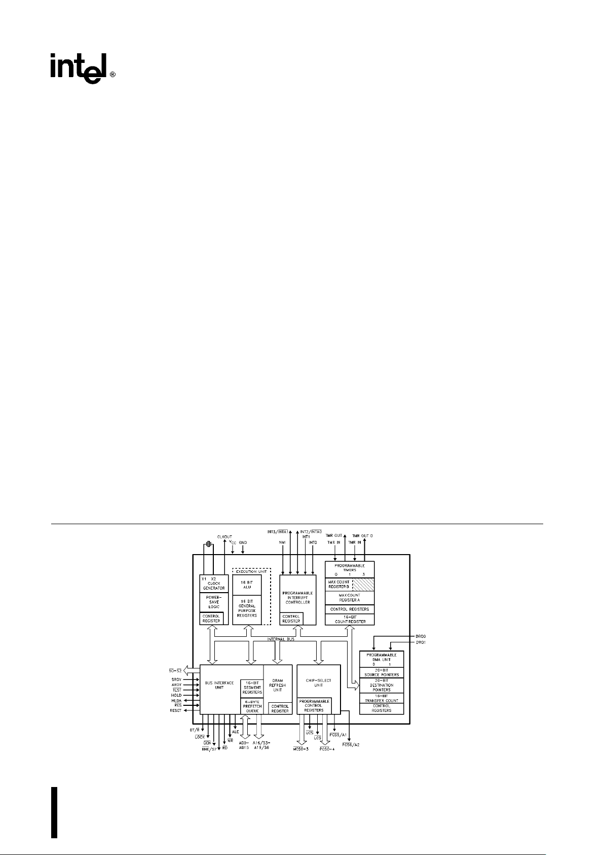
270500–1
Figure 1. M80C186 Block Diagram
Page 2
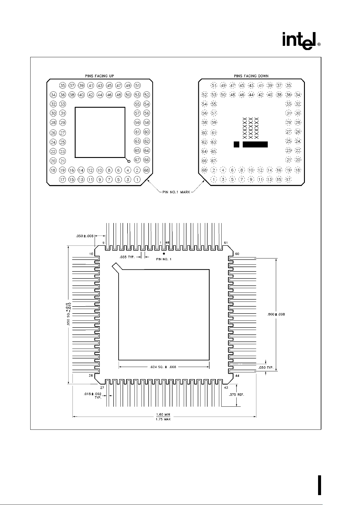
M80C186
Pin Grid Array
270500–30
Quad Flat Pack
270500–31
Figure 2. M80C186 Pinout Diagram
For additional packaging information refer to ‘‘Packaging Outlines and Dimensions’’, Order Number 231369
2
Page 3
M80C186
Table 1. M80C186 Pin Description
Symbol PGA QFP Type Name and Function
VCC,V
CC
9, 43 1, 35 I System Power:a5 volt power supply.
VSS,V
SS
26, 60 52, 18 I System Ground.
RESET 57 21 O Reset Output indicates that the M80C186 CPU is being
reset, and can be used as a system reset. It is active HIGH,
synchronized with the processor clock, and lasts an integer
number of clock periods corresponding to the length of the
RES
signal. Reset goes inactive 2 clockout periods after
RES
goes inactive. When tied to the TEST/BUSY pin, Reset
forces the M80C186 into enhanced mode.
X1, X2 59, 58 19, 20 I Crystal Inputs X1 and X2 provide external connections for a
fundamental mode or third overtone parallel resonant crystal
for the internal oscillator. X1 can connect to an external
clock instead of a crystal. In this case, minimize the
capacitance on X2 or drive X2 with complemented X1. The
input or oscillator frequency is internally divided by two to
generate the clock signal (CLKOUT).
CLKOUT 56 22 O Clock Output provides the system with a 50% duty cycle
waveform. All device pin timings are specified relative to
CLKOUT. CLKOUT has sufficient MOS drive capabilities for
the Numeric Processor Extension.
RES 24 54 I System Reset causes the M80C186 to immediately
terminate its present activity, clear the internal logic, and
enter a dormant state. This signal may be asynchronous to
the M80C186 clock. The M80C186 begins fetching
instructions approximately 7 clock cycles after RES is
returned HIGH. For proper initialization, V
CC
must be within
specifications and the clock signal must be stable for more
than 4 clocks with RES
held LOW. RES is internally
synchronized. This input is provided with a Schmitt-trigger to
facilitate power-on RES
generation via an RC network. When
RES
occurs, the M80C186 will drive the status lines to an
inactive level for one clock, and then float them.
TEST/BUSY 47 31 I The TEST pin is sampled during and after reset to determine
whether the M80C186 is to enter Compatible or Enhanced
Mode. Enhanced Mode requires TEST
to be HIGH on the
rising edge of RES
and LOW four clocks later. Any other
combination will place the M80C186 in Compatible Mode. A
weak internal pullup insures a HIGH state when the pin is not
driven.
TEST
ÐIn Compatible Mode this pin is configured to operate
as TEST
. This pin is examined by the WAIT instruction. If the
TEST
input is HIGH when WAIT execution begins, instruction
execution will suspend. TEST
will be resampled every five
clocks until it goes LOW, at which time execution will resume.
If interrupts are enabled while the M80C186 is waiting for
TEST
, interrupts will be serviced.
BUSYÐIn Enhanced Mode, this pin is configured to operate
as BUSY. The BUSY input is used to notify the M80C186 of
Numerics Processor Extension activity. Floating point
instructions executing in the M80C186 sample the BUSY pin
to determine when the Numerics Processor is ready to
accept a new command. BUSY is active HIGH.
3
Page 4
M80C186
Table 1. M80C186 Pin Description (Continued)
Symbol PGA QFP Type Name and Function
TMR IN 1
TMR IN 0, 20
21
58
57 I
I Timer Inputs are used either as clock or control signals,
depending upon the programmed timer mode. These inputs
are active HIGH (or LOW-to-HIGH transitions are counted) and
internally synchronized.
TMR OUT 0,
TMR OUT 1 23
22 56
55 O
O Timer outputs are used to provide single pulse or continous
waveform generation, depending upon the timer mode
selected.
DRQ1
DRQ0 18
19 59
60 I
I
DMA Request is driven HIGH by an external device when it
desires that a DMA channel (Channel 0 or 1) perform a
transfer. These signals are active HIGH, level-triggered, and
internally synchronized.
NMI 46 32 I Non-Maskable Interrupt is an edge-triggered input which
causes a type 2 interrupt. NMI is not maskable internally. A
transition from a LOW to HIGH initiates the interrupt at the
next instruction boundary. NMI is latched internally. An NMI
duration of one clock or more will guarantee service. This input
is internally synchronized.
INT0, INT1
INT3/INTA1
INT2/INTA0
45, 44
41
42
33, 34
37
36
I/O
I/O
I Maskable Interrupt Requests can be requested by activating
one of these pins. When configured as inputs, these pins are
active HIGH. Interrupt Requests are synchronized internally.
INT2 and INT3 may be configured via software to provide
active-LOW interrupt-acknowledge output signals. All interrupt
inputs may be configured via software to be either edge- or
level-triggered. To ensure recognition, all interrupt requests
must remain active until the interrupt is acknowledged. When
slave mode is selected, the function of these pins changes
(see Interrupt Controller section of this data sheet).
A19/S6,
A16/S3
A17/S4,
A18/S5,
65
68
67
66
13
10
11
12
O
O
O
O
Address Bus Outputs (16 –19) and Bus Cycle Status (3 –6)
reflect the four most significant address bits during T1. These
signals are active HIGH. During T
2,T3,TW
, and T4, status
information is available on these lines as encoded below:
Low High
S6 Processor Cycle DMA Cycle
S3, S4, and S5 are defined as LOW during T2–T4.
AD15 1 9 I/O Address/Data Bus (0– 15) signals constitute the time
multiplexed memory or I/O address (T
1
) and data (T2,T3,TW,
AD14 3 7
and T
4
) bus. The
AD13 5 5
AD12 7 3 bus is active HIGH. A
0
is analogous to BHE for the lower byte
of the data bus, pins D
7
through D0. It is LOW during T1when
AD11 10 68
a byte is to be transferred onto the lower portion of the bus in
AD10 12 66
memory or I/O operations.
AD9 14 64
AD8 16 62
AD7 2 8
AD6 4 6
AD5 6 4
AD4 8 2
AD3 11 67
AD2 13 65
AD1 15 63
AD0 17 61
4
Page 5
M80C186
Table 1. M80C186 Pin Description (Continued)
Symbol PGA QFP Type Name and Function
BHE 64 14 O The BHE (Bus High Enable) signal is analogous to A0 in that
it is used to enable data on to the most significant half of the
data bus, pins D15 –D8. BHE
will be LOW during T1when the
upper byte is transferred and will remain LOW through T
3
AND TW. BHE does not need to be latched. BHE will float
during HOLD.
In Enhanced Mode, BHE will also be used to signify DRAM
refresh cycles. A refresh cycle is indicated by BHE
and A0
being HIGH.
BHE and A0 Encodings
BHE Value A0 Value Function
0 0 Word Transfer
0 1 Byte Transfer on upper half
of data bus (D15 –D8)
1 0 Byte Transfer on lower half
of data bus (D
7–D0
)
1 1 Refresh
ALE/QS0 61 17 O Address Latch Enable/Queue Status 0 is provided by the
M80C186 to latch the address. ALE is active HIGH.
Addresses are guaranteed to be valid on the trailing edge of
ALE. The ALE rising edge is generated off the rising edge of
the CLKOUT immediately preceding T1of the associated bus
cycle, effectively one-half clock cycle earlier than in the
standard M8086. The trailing edge is generated off the
CLKOUT rising edge in T
1
as in the M8086. Note that ALE is
never floated.
WR/QS1 63 15 O Write Strobe/Queue Status 1 indicates that the data on the
bus is to be written into a memory or an I/O device. WR
is
active for T
2,T3
, and TWof any write cycle. It is active LOW,
and floats during ‘‘HOLD.’’ It is driven HIGH for one clock
during Reset, and then floated. When the M80C186 is in
queue status mode, the ALE/QS0 and WR
/QS1 pins provide
information about processor/instruction queue interaction.
QS1 QS0 Queue Operation
0 0 No queue operation
0 1 First opcode byte fetched
from the queue
1 1 Subsequent byte fetched
from the queue
1 0 Empty the queue
RD/QSMD 62 16 O Read Strobe indicates that the M80C186 is performing a
memory or I/O read cycle. RD
is active LOW for T2,T3, and
T
W
of any read cycle. It is guaranteed not to go LOW in T
2
until after the Address Bus is floated. RD is active LOW, and
floats during ‘‘HOLD’’. RD is driven HIGH for one clock
during Reset, and then the output driver is floated. A weak
internal pull-up mechanism of the RD
line holds it HIGH when
the line is not driven. During RESET the pin is sampled to
determine whether the M80C186 should provide ALE, WR
and RD, or if the Queue-Status should be provided. RD
should be connected to GND to provide Queue-Status data.
5
Page 6
M80C186
Table 1. M80C186 Pin Description (Continued)
Symbol PGA QFP Type Name and Function
ARDY 55 23 I Asynchronous Ready informs the M80C186 that the
addressed memory space or I/O device will complete
a data transfer. The ARDY input pin will accept an
asynchronous input, and is active HIGH. Only the rising
edge is internally synchronized by the M80C186. This
means that the falling edge of ARDY must be
synchronized to the M80C186 clock. If connected to
V
CC
, no WAIT states are inserted. Asynchronous ready
(ARDY) or synchronous ready (SRDY) must be active
to terminate a bus cycle. If unused, this line should be
tied LOW to yield control to the SRDY pin.
SRDY 49 29 I Synchronous Ready must be synchronized externally
to the M80C186. The use of SRDY provides a relaxed
system-timing specification on the Ready input. This is
accomplished by eliminating the one-half clock cycle
which is required for internally resolving the signal level
when using the ARDY input. This line is active HIGH. If
this line is connected to V
CC
, no WAIT states are
inserted. Asynchronous ready (ARDY) or synchronous
ready (SRDY) must be active before a bus cycle is
terminated. If unused, this line should be tied LOW to
yield control to the ARDY pin.
LOCK 48 30 O LOCK output indicates that other system bus masters
are not to gain control of the system bus while LOCK
is
active LOW. The LOCK
signal is requested by the
LOCK prefix instruction and is activated at the
beginning of the first data cycle associated with the
instruction following the LOCK prefix. It remains active
until the completion of the instruction following the
LOCK prefix. No prefetches will occur while LOCK is
asserted. LOCK
is active LOW, is driven HIGH for one
clock during RESET, and then floated.
S0,S1,S2 52, 53, 54 26, 25, 24 O Bus cycle status S0–S2 are encoded to provide bus-
transaction information:
M80C186 Bus Cycle Status Information
S2 S1 S0 Bus Cycle Initiated
0 0 0 Interrupt Acknowledge
0 0 1 Read I/O
0 1 0 Write I/O
0 1 1 Halt
1 0 0 Instruction Fetch
1 0 1 Read Data from Memory
1 1 0 Write Data to Memory
1 1 1 Passive (no bus cycle)
The status pins float during HOLD/HLDA.
S2
may be used as a logical M/IO indicator, and S1 as
a DT/R
indicator.
The status lines are driven HIGH for one clock during
Reset, and then floated until a bus cycle begins.
6
Page 7
M80C186
Table 1. M80C186 Pin Description (Continued)
Symbol PGA QFP Type Name and Function
HLDA (output)
HOLD (input)
51
50
27
28
O
I HOLD indicates that another bus master is requesting the
local bus. The HOLD input is active HIGH. HOLD may be
asynchronous with respect to the M80C186 clock. The
M80C186 will issue a HLDA (HIGH) in response to a HOLD
request at the end of T
4
or Ti. Simultaneous with the
issuance of HLDA, the M80C186 will float the local bus and
control lines. After HOLD is detected as being LOW, the
M80C186 will lower HLDA. When the M80C186 needs to
run another bus cycle, it will again drive the local bus and
control lines.
In Enhanced Mode, HLDA will go low when a DRAM
refresh cycle is pending in the M80C186 and an external
bus master has control of the bus. It will be up to the
external master to relinquish the bus by lowering HOLD so
that the M80C186 may execute the refresh cycle. Lowering
HOLD for four clocks and returning HIGH will insure only
one refresh cycle to the external master. HLDA will
immediately go active after the refresh cycle has taken
place.
UCS 34 44 O Upper Memory Chip Select is an active LOW output
whenever a memory reference is made to the defined
upper portion (1K– 256K block) of memory. This line is not
floated during bus HOLD. The address range activating
UCS
is software programmable.
UCS and LCS are sampled upon the rising edge of RES.If
both pins are held low, the M80C186 will enter ONCE
Mode. In ONCE Mode all pins assume a high impedance
state and remain so until a subsequent RESET. UCS
has a
weak internal pullup for normal operation.
LCS 33 45 O Lower Memory Chip Select is active LOW whenever a
memory reference is made to the defined lower portion
(1K– 256K) of memory. This line is not floated during bus
HOLD. The address range activating LCS
is software
programmable.
UCS
and LCS are sampled upon the rising edge of RES.If
both pins are held low, the M80C186 will enter ONCE
Mode. In ONCE Mode all pins assume a high impedance
state and remain so until a subsequent RESET. UCS
has a
weak internal pullup for normal operation.
MCS0/PEREQ 38 40 I/O Mid-Range Memory Chip Select signals are active LOW
MCS1
/ERROR 37 41 I/O when a memory reference is made to the defined mid-
MCS2
36 42 O range portion of memory (8K – 512K). These lines are not
MCS3
/NPS 35 43 O floated during bus HOLD. The address ranges activating
MCS0
–3 are software programmable.
In Enhanced Mode, MCS0 becomes a PEREQ input
(Processor Extension Request). When connected to the
Numerics Processor Extension, this input is used to signal
the M80C186 when to make numeric data transfers to and
from the NPX. MCS3 becomes NPS (Numeric Processor
Select) which may only be activated by communication to
the Numerics Processor Extension. MCS1
becomes
ERROR in enhanced mode and is used to signal numerics
coprocessor errors.
7
Page 8
M80C186
Table 1. M80C186 Pin Description (Continued)
Symbol PGA QFP Type Name and Function
PCS0
PCS1–4 27, 28, 29, 302551, 50, 49, 48
53
O
O Peripheral Chip Select signals 0 –4 are active LOW
when a reference is made to the defined peripheral
area (64K byte I/O space). These lines are not floated
during bus HOLD. The address ranges activating
PCS0
–4 are software programmable.
PCS5/A1 31 47 O Peripheral Chip Select 5 or Latched A1 may be
programmed to provide a sixth peripheral chip select, or
to provide an internally latched A1 signal. The address
range activating PCS5
is software programmable. When
programmed to provide latched. A1, rather than PCS5
,
this pin will retain the previously latched value of A1
during a bus HOLD. A1 is active HIGH.
PCS6/A2 32 46 O Peripheral Chip Select 6 or Latched A2 may be
programmed to provide a seventh peripheral chip
select, or to provide an internally latched A2 signal. The
address range activating PCS6
is software
programmable. When programmed to provide latched
A2, rather than PCS6
, this pin will retain the previously
latched value of A2 during a bus HOLD. A2 is active
HIGH.
DT/R 40 38 O Data Transmit/Receive controls the direction of data
flow through the external M8286/M8287 data bus
transceiver. When LOW, data is transferred to the
M80C186. When HIGH the M80C186 places write data
on the data bus.
DEN 39 39 O Data Enable is provided as an M8286/M8287 data bus
transceiver output enable. DEN
is active LOW during
each memory and I/O access. DEN
is HIGH whenever
DT/R
changes state.
8
Page 9

M80C186
FUNCTIONAL DESCRIPTION
Introduction
The following Functional Description describes the
base architecture of the M80C186. This architecture
is common to the M8086, M8088, M80186 and
M80286 microprocessor families as well. The
M80C186 is a very high integration 16-bit microprocessor. It combines 15 –20 of the most common microprocessor system components onto one chip.
The M80C186 is object code compatible with the
M8086/M8088 microprocessors and adds 10 new
instruction types to the existing M8086/M8088 instruction set.
The M80C186 has two major modes of operation,
Compatible and Enhanced. In Compatible Mode the
M80C186 is completely compatible with NMOS
M80186, with the exception of M8087 support. All
pin functions, timings, and drive capabilities are
identical. The Enhanced mode adds three new features to the system design. These are Power-Save
control, Dynamic RAM refresh, and an asynchronous Numerics Co-processor interface.
M80C186 BASE ARCHITECTURE
The M8086, M8088, M80186, and M80286 family all
contain the same basic set of registers, instructions,
and addressing modes. The M80C186 processor is
upward compatible with the M8086, M8088, and
M80286 CPUs.
Register Set
The M80C186 base architecture has fourteen registers as shown in Figures 3a and 3b. These registers
are grouped into the following categories.
General Registers
Eight 16-bit general purpose registers may be used
to contain arithmetic and logical operands. Four of
these (AX, BX, CX, and DX) can be used as 16-bit
registers or split into pairs of separate 8-bit registers.
Segment Registers
Four 16-bit special purpose registers select, at any
given time, the segments of memory that are immediately addressable for code, stack, and data. (For
usage, refer to Memory Organization.)
Base and Index Registers
Four of the general purpose registers may also be
used to determine offset addresses of operands in
memory. These registers may contain base addresses or indexes to particular locations within a segment. The addressing mode selects the specific registers for operand and address calculations.
Status and Control Registers
Two 16-bit special purpose registers record or alter
certain aspects of the M80C186 processor state.
These are the Instruction Pointer Register, which
contains the offset address of the next sequential
instruction to be executed, and the Status Word
Register, which contains status and control flag bits
(see Figures 3a and 3b).
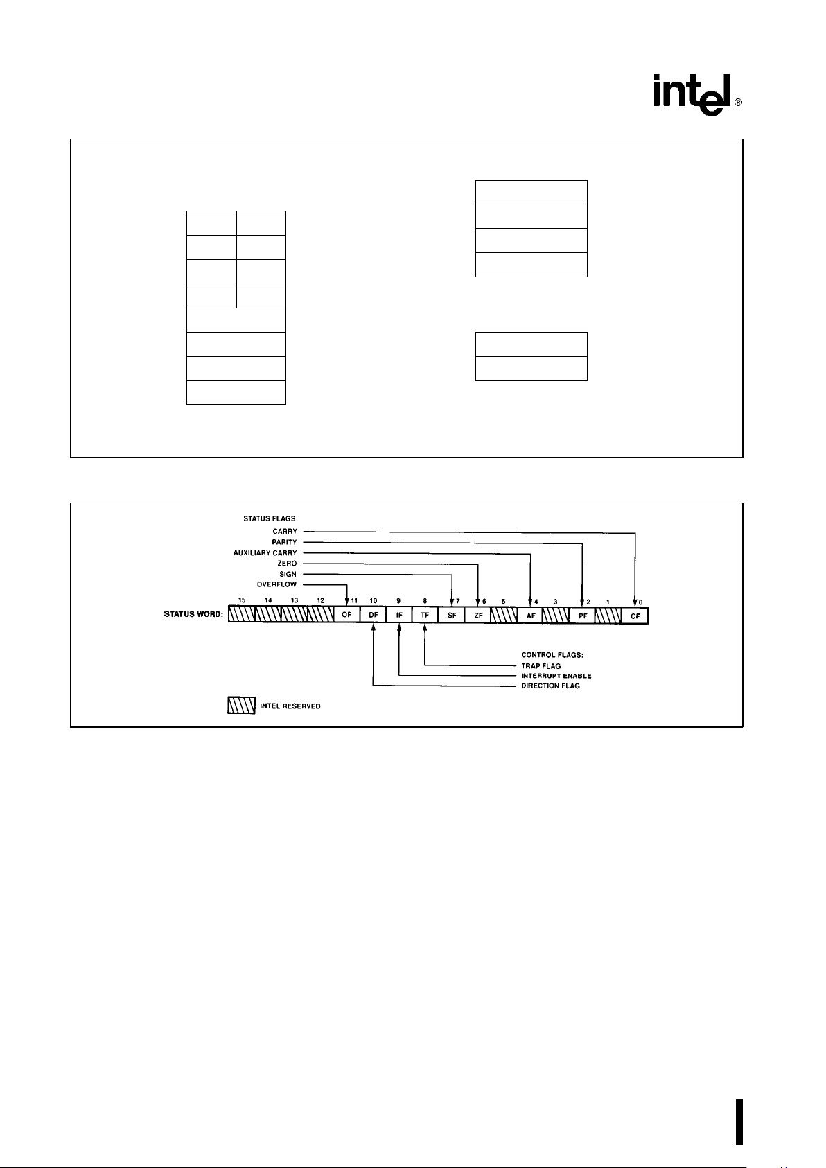
Status Word Description
The Status Word records specific characteristics of
the result of logical and arithmetic instructions (bits
0, 2, 4, 6, 7, and 11) and controls the operation of
the M80C186 within a given operating mode (bits 8,
9, and 10). The Status Word Register is 16-bits wide.
The function of the Status Word bits is shown in
Table 2.
9
Page 10
M80C186
16-BIT SPECIAL
REGISTER REGISTER
NAME FUNCTIONS
7070
BYTE
ADDRESSABLE
AX AH AL
MULTIPLY/DIVIDE
REGISTER
(8-BIT
DX DH DL
I/O INSTRUCTIONS
*
SHOWN)
NAMES
CX CH CL
(
LOOP/SHIFT/REPEAT/COUNT
%
BX BH BL
BASE REGISTERS
BP
*
SI
INDEX REGISTERS
DI
*
SP
(
STACK POINTER
15 0
GENERAL
REGISTERS
15 0
CS CODE SEGMENT SELECTOR
DS DATA SEGMENT SELECTOR
SS STACK SEGMENT SELECTOR
ES EXTRA SEGMENT SELECTOR
SEGMENT REGISTERS
15 0
F STATUS WORD
IP INSTRUCTION POINTER
STATUS AND CONTROL
REGISTERS
Figure 3a. M80C186 Register Set
270500–4
Figure 3b. Status Word Format
10
Page 11

M80C186
Table 2. Status Word Bit Functions
Bit
Name Function
Position
0 CF Carry FlagÐSet on high-order
bit carry or borrow; cleared
otherwise
2 PF Parity FlagÐSet if low-order 8
bits of result contain an even
number of 1-bits; cleared
otherwise
4 AF Set on carry from or borrow to
the low order four bits of AL;
cleared otherwise
6 ZF Zero FlagÐSet if result is zero;
cleared otherwise
7 SF Sign FlagÐSet equal to high-
order bit of result (0 if positive,
1 if negative)
8 TF Single Step FlagÐOnce set, a
single step interrupt occurs
after the next instruction
executes. TF is cleared by the
single step interrupt.
9 IF Interrupt-enable FlagÐWhen
set, maskable interrupts will
cause the CPU to transfer
control to an interrupt vector
specified location.
10 DF Direction FlagÐCauses string
instructions to auto decrement
the appropriate index register
when set. Clearing DF causes
auto increment.
11 OF Overflow FlagÐSet if the
signed result cannot be
expressed within the number
of bits in the destination
operand; cleared otherwise
Instruction Set
The instruction set is divided into seven categories:
data transfer, arithmetic, shift/rotate/logical, string
manipulation, control transfer, high-level instructions, and processor control. These categories are
summarized in Figure 4.
An M80C186 instruction can reference anywhere
from zero to several operands. An operand can reside in a register, in the instruction itself, or in memory. Specific operand addressing modes are discussed later in this data sheet.
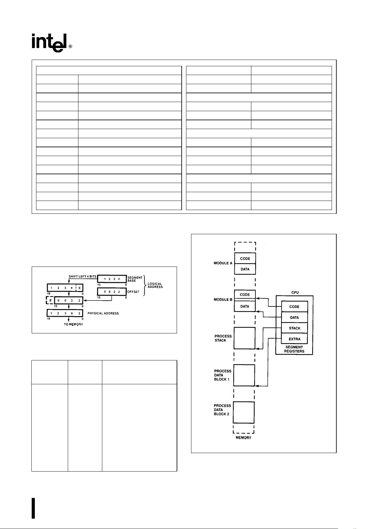
Memory Organization
Memory is organized in sets of segments. Each segment is a linear contiguous sequence of up to 64K
(2
16
) 8-bit bytes. Memory is addressed using a twocomponent address (a pointer) that consists of a 16bit base segment and a 16-bit offset. The 16-bit
base values are contained in one of four internal
segment register (code, data, stack, extra). The
physical address is calculated by shifting the base
value LEFT by four bits and adding the 16-bit offset
value to yield a 20-bit physical address (see Figure
5). This allows for a 1 MByte physical address size.
All instructions that address operands in memory
must specify the base segment and the 16-bit offset
value. For speed and compact instruction encoding,
the segment register used for physical address generation is implied by the addressing mode used (see
Table 3). These rules follow the way programs are
written (see Figure 6) as independent modules that
require areas for code and data, a stack, and access
to external data areas.
Special segment override instruction prefixes allow
the implicit segment register selection rules to be
overridden for special cases. The stack, data, and
extra segments may coincide for simple programs.
11
Page 12
M80C186
GENERAL PURPOSE
MOV Move byte or word
PUSH Push word onto stack
POP Pop word off stack
PUSHA Push all registers on stack
POPA Pop all registers from stack
XCHG Exchange byte or word
XLAT Translate byte
INPUT/OUTPUT
IN Input byte or word
OUT Output byte or word
ADDRESS OBJECT
LEA Load effective address
LDS Load pointer using DS
LES Load pointer using ES
FLAG TRANSFER
LAHF Load AH register from flags
SAHF Store AH register in flags
PUSHF Push flags onto stack
POPF Pop flags off stack
ADDITION
ADD Add byte or word
ADC Add byte or word with carry
INC Increment byte or word by 1
AAA ASCII adjust for addition
DAA Decimal adjust for addition
SUBTRACTION
SUB Subtract byte or word
SBB Subtract byte or word with borrow
DEC Decrement byte or word by 1
NEG Negate byte or word
CMP Compare byte or word
AAS ASCII adjust for subtraction
DAS Decimal adjust for subtraction
MULTIPLICATION
MUL Multiply byte or word unsigned
IMUL Integer multiply byte or word
AAM ASCII adjust for multiplyASCII
DIVISION
DIV Divide byte or word unsigned
IDIV Integer divide byte or word
AAD ASCII adjust for division
CBW Convert byte to word
CWD Convert word to doubleword
MOVS Move byte or word string
INS Input bytes or word string
OUTS Output bytes or word string
CMPS Compare byte or word string
SCAS Scan byte or word string
LODS Load byte or word string
STOS Store byte or word string
REP Repeat
REPE/REPZ Repeat while equal/zero
REPNE/REPNZ Repeat while not equal/not zero
LOGICALS
NOT ‘‘Not’’ byte or word
AND ‘‘And’’ byte or word
OR ‘‘Inclusive or’’ byte or word
XOR ‘‘Exclusive or’’ byte or word
TEST ‘‘Test’’ byte or word
SHIFTS
SHL/SAL Shift logical/arithmetic left byte or word
SHR Shift logical right byte or word
SAR Shift arithmetic right byte or word
ROTATES
ROL Rotate left byte or word
ROR Rotate right byte or word
RCL Rotate through carry left byte or word
RCR Rotate through carry right byte or word
FLAG OPERATIONS
STC Set carry flag
CLC Clear carry flag
CMC Complement carry flag
STD Set direction flag
CLD Clear direction flag
STI Set interrupt enable flag
CLI Clear interrupt enable flag
EXTERNAL SYNCHRONIZATION
HLT Halt until interrupt or reset
WAIT Wait for TEST pin active
ESC Escape to extension processor
LOCK Lock bus during next instruction
NO OPERATION
NOP No operation
HIGH LEVEL INSTRUCTIONS
ENTER Format stack for procedure entry
LEAVE Restore stack for procedure exit
BOUND Detects values outside prescribed range
Figure 4. M80C186 Instruction Set
12
Page 13
M80C186
CONDITIONAL TRANSFERS
JA/JNBE Jump if above/not below nor equal
JAE/JNB Jump if above or equal/not below
JB/JNAE Jump if below/not above nor equal
JBE/JNA Jump if below or equal/not above
JC Jump if carry
JE/JZ Jump if equal/zero
JG/JNLE Jump if greater/not less nor equal
JGE/JNL Jump if greater or equal/not less
JL/JNGE Jump if less/not greater nor equal
JLE/JNG Jump if less or equal/not greater
JNC Jump if not carry
JNE/JNZ Jump if not equal/not zero
JNO Jump if not overflow
JNP/JPO Jump if not parity/parity odd
JNS Jump if not sign
JO Jump if overflow
JP/JPE Jump if parity/parity even
JS Jump if sign
UNCONDITIONAL TRANSFERS
CALL Call procedure
RET Return from procedure
JMP Jump
ITERATION CONTROLS
LOOP Loop
LOOPE/LOOPZ Loop if equal/zero
LOOPNE/LOOPNZ Loop if not equal/not zero
JCXZ Jump if register CXe0
INTERRUPTS
INT Interrupt
INTO Interrupt if overflow
IRET Interrupt return
Figure 4. M80C186 Instruction Set (Continued)
To access operands that do not reside in one of the
four immediately available segments, a full 32-bit
pointer can be used to reload both the base (segment) and offset values.
270500–5
Figure 5. Two Component Address
Table 3. Segment Register Selection Rules
Memory Segment
Implicit Segment
Reference Register
Selection Rule
Needed Used
Instructions Code (CS) Instruction prefetch and
immediate data.
Stack Stack (SS) All stack pushes and
pops; any memory
references which use BP
Register as a base
register.
External Extra (ES) All string instruction
Data references which use
(Global) the DI register as an
index.
Local Data Data (DS) All other data references.
270500–6
Figure 6. Segmented Memory Helps
Structure Software
13
Page 14

M80C186
Addressing Modes
The M80C186 provides eight categories of addressing modes to specify operands. Two addressing
modes are provided for instructions that operate on
register or immediate operands:
#
Register Operand Mode:
The operand is located
in one of the 8- or 16-bit general registers.
#
Immediate Operand Mode:
The operand is in-
cluded in the instruction.
Six modes are provided to specify the location of an
operand in a memory segment. A memory operand
address consists of two 16-bit components: a segment base and an offset. The segment base is supplied by a 16-bit segment register either implicitly
chosen by the addressing mode or explicitly chosen
by a segment override prefix. The offset, also called
the effective address, is calculated by summing any
combination of the following three address elements:
#
the
displacement
(an 8- or 16-bit immediate value
contained in the instruction);
#
the
base
(contents of either the BX or BP base
registers); and
#
the
index
(contents of either the SI or DI index
registers).
Any carry out from the 16-bit addition is ignored.
Eight-bit displacements are sign extended to 16-bit
values.
Combinations of these three address elements define the six memory addressing modes, described
below.
#
Direct Mode:
The operand’s offset is contained in
the instruction as an 8- or 16-bit displacement element.
#
Register Indirect Mode:
The operand’s offset is in
one of the registers SI, DI, BX, or BP.
#
Based Mode:
The operand’s offset is the sum of
an 8- or 16-bit displacement and the contents of
a base register (BX or BP).
#
Indexed Mode:
The operand’s offset is the sum
of an 8- or 16-bit displacement and the contents
of an index register (SI or DI).
#
Based Indexed Mode:
The operand’s offset is the
sum of the contents of a base register and an
Index register.
#
Based indexed Mode with Displacement:
The operand’s offset is the sum of a base register’s contents, an index register’s contents, and an 8- or
16-bit displacement.
Data Types
The M80C186 directly supports the following data
types:
#
Integer:
A signed binary numeric value contained
in an 8-bit byte or a 16-bit word. All operations
assume a 2’s complement representation.
Signed 32- and 64-bit integers are supported using a Numeric Data Coprocessor with the
M80C186.
#
Ordinal:
An unsigned binary numeric value con-
tained in an 8-bit byte or a 16-bit word.
#
Pointer:
A 16- or 32-bit quantity, composed of a
16-bit offset component or a 16-bit segment base
component in addition to a 16-bit offset component.
#
String:
A contiguous sequence of bytes or words.
A string may contain from 1 to 64K bytes.
#
ASCII:
A byte representation of alphanumeric and
control characters using the ASCII standard of
character representation.
#
BCD:
A byte (unpacked) representation of the
decimal digits 0 – 9.
#
Packed BCD:
A byte (packed) representation of
two decimal digits (0– 9). One digit is stored in
each nibble (4-bits) of the byte.
#
Floating Point:
A signed 32-, 64-, or 80-bit real
number representation. (Floating point operands
are supported using a Numeric Data Coprocessor
with the M80C186.)
In general, individual data elements must fit within
defined segment limits. Figure 7 graphically represents the data types supported by the M80C186.
I/O Space
The I/O space consists of 64K 8-bit or 32K 16-bit
ports. Separate instructions address the I/O space
with either an 8-bit port address, specified in the instruction, or a 16-bit port address in the DX register.
8-bit port addresses are zero extended such that
A
15–A8
are LOW. I/O port addresses 00F8(H)
through 00FF(H) are reserved.
Interrupts
An interrupt transfers execution to a new program
location. The old program address (CS:IP) and machine state (Status Word) are saved on the stack to
allow resumption of the interrupted program. Interrupts fall into three classes: hardware initiated, INT
instructions, and instruction exceptions. Hardware
initiated interrupts occur in response to an external
input and are classified as non-maskable or maskable.
14
Page 15
M80C186
270500–7
NOTE:
*Supported by using a Numeric Data Coprocessor with
the M80C186.
Figure 7. M80C186 Supported Data Types
Programs may cause an interrupt with an INT instruction. Instruction exceptions occur when an unusual condition, which prevents further instruction
processing, is detected while attempting to execute
an instruction. If the exception was caused by executing an ESC instruction with the ESC trap bit set in
the relocation register, the return instruction will
point to the ESC instruction, or to the segment override prefix immediately preceding the ESC instruc-
tion if the prefix was present. In all other cases, the
return address from an exception will point at the
instruction immediately following the instruction
causing the exception.
A table containing up to 256 pointers defines the
proper interrupt service routine for each interrupt. Interrupts 0– 31, some of which are used for instruction exceptions, are reserved. Table 4 shows the
M80C186 predefined types and default priority levels. For each interrupt, an 8-bit vector must be supplied to the M80C186 which identifies the appropriate table entry. Exceptions supply the interrupt
vector internally. In addition, internal peripherals and
noncascaded external interrupts will generate their
own vectors through the internal interrupt controller.
INT instructions contain or imply the vector and allow access to all 256 interrupts. Maskable hardware
initiated interrupts supply the 8-bit vector to the CPU
during an interrupt acknowledge bus sequence.
Non-maskable hardware interrupts use a predefined
internally supplied vector.
Interrupt Sources
The M80C186 can service interrupts generated by
software or hardware. The software interrupts are
generated by specific instructions (INT, ESC, unused
OP, etc.) or the results of conditions specified by
instructions (array bounds check, INT0, DIV, IDIV,
etc.). All interrupt sources are serviced by an indirect
call through an element of a vector table. This vector
table is indexed by using the interrupt vector type
(Table 4), multiplied by four. All hardware-generated
interrupts are sampled at the end of each instruction. Thus, the software interrupts will begin service
first. Once the service routine is entered and interrupts are enabled, any hardware source of sufficient
priority can interrupt the service routine in progress.
The software generated M80C186 interrupts are described below.
DIVIDE ERROR EXCEPTION (TYPE 0)
Generated when a DIV or IDIV instruction quotient
cannot be expressed in the number of bits in the
destination.
SINGLE-STEP INTERRUPT (TYPE 1)
Generated after most instructions if the TF flag is
set. Interrupts will not be generated after prefix instructions (e.g., REP), instructions which modify segment registers (e.g., POP DS), or the WAIT instruction.
NON-MASKABLE INTERRUPTÐNMI (TYPE 2)
An external interrupt source which cannot be
masked.
15
Page 16
M80C186
Table 4. M80C186 Interrupt Vectors
Interrupt Vector Default Related
Name Type Priority
(4)
Instructions
Divide Error 0 1
(1)
DIV, IDIV
Exception
Single Step 1 12
(2)
All
Interrupt
NMI 2 1 All
Breakpoint 3 1
(1)
INT
Interrupt
INT0 Detected 4 1
(1)
INT0
Overflow
Exception
Array Bounds 5 1
(1)
BOUND
Exception
Unused-Opcode 6 1
(1)
Undefined
Exception Opcodes
ESC Opcode 7 1
(1), (5)
ESC Opcodes
Exception
Timer 0 Interrupt 8 2A
(3)
Timer 1 Interrupt 18 2B
(3)
Timer 2 Interrupt 19 2C
(3)
Reserved 9 3
DMA 0 Interrupt 10 4
DMA 1 Interrupt 11 5
INT0 Interrupt 12 6
INT1 Interrupt 13 7
INT2 Interrupt 14 8
INT3 Interrupt 15 9
NOTES:
1. These are generated as the result of an instruction execution.
2. This is handled as in the M8086.
3. All three timers constitute one source of request to the
interrupt controller. The Timer interrupts all have the same
default priority level with respect to all other interrupt
sources. However, they have a defined priority ordering
amongst themselves. (Priority 2A is higher priority than 2B.)
Each Timer interrupt has a separate vector type number.
4. Default priorities for the interrupt sources are used only if
the user does not program each source into a unique priority level.
5. An escape opcode will cause a trap if the M80C186 is in
compatible mode or if the processor is in enhanced mode
with the proper bit set in the peripheral control block relocation register.
BREAKPOINT INTERRUPT (TYPE 3)
A one-byte version of the INT instruction. It uses 12
as an index into the service routine address table
(because it is a type 3 interrupt).
INT0 DETECTED OVERFLOW EXCEPTION
(TYPE4)
Generated during an INT0 instruction if the 0F bit is
set.
ARRAY BOUNDS EXCEPTION (TYPE 5)
Generated during a BOUND instruction if the array
index is outside the array bounds. The array bounds
are located in memory at a location indicated by one
of the instruction operands. The other operand indicates the value of the index to be checked.
UNUSED OPCODE EXCEPTION (TYPE 6)
Generated if execution is attempted on undefined
opcodes.
ESCAPE OPCODE EXCEPTION (TYPE 7)
Generated if execution is attempted of ESC opcodes
(D8H– DFH). In compatible mode operation, ESC
opcodes will always generate this exception. In enhanced mode operation, the exception will be generated only if a bit in the relocation register is set. The
return address of this exception will point to the ESC
instruction causing the exception. If a segment override prefix preceded the ESC instruction, the return
address will point to the segment override prefix.
Hardware-generated interrupts are divided into two
groups: maskable interrupts and non-maskable interrupts. The M80C186 provides maskable hardware
interrupt request pins INT0 –INT3. In addition, maskable interrupts may be generated by the M80C186
integrated DMA controller and the integrated timer
unit. The vector types for these interrupts is shown
in Table 4. Software enables these inputs by setting
the interrupt flag bit (IF) in the Status Word. The interrupt controller is discussed in the peripheral section of this data sheet.
Further maskable interrupts are disabled while servicing an interrupt because the IF bit is reset as part
of the response to an interrupt or exception. The
saved Status Word will reflect the enable status of
the processor prior to the interrupt. The interrupt flag
will remain zero unless specifically set. The interrupt
return instruction restores the Status Word, thereby
restoring the original status of IF bit. If the interrupt
return re-enables interrupts, and another interrupt is
pending, the M80C186 will immediately service the
highest-priority interrupt pending, i.e., no instructions
of the main line program will be executed.
Non-Maskable Interrupt Request (NMI)
A non-maskable interrupt (NMI) is also provided.
This interrupt is serviced regardless of the state of
the IF bit. A typical use of NMI would be to activate a
power failure routine. The activation of this input
causes an interrupt with an internally supplied vector
value of 2. No external interrupt acknowledge sequence is performed. The IF bit is cleared at the
beginning of an NMI interrupt to prevent maskable
interrupts from being serviced.
16
Page 17

M80C186
Single-Step Interrupt
The M80C186 has an internal interrupt that allows
programs to execute one instruction at a time. It is
called the single-step interrupt and is controlled by
the single-step flag bit (TF) in the Status Word. Once
this bit is set, an internal single-step interrupt will
occur after the next instruction has been executed.
The interrupt clears the TF bit and uses an internally
supplied vector of 1. The IRET instruction is used to
set the TF bit and transfer control to the next instruction to be single-stepped.
Initialization and Processor Reset
Processor initialization or startup is accomplished by
driving the RES
input pin LOW. RES forces the
M80C186 to terminate all execution and local bus
activity. No instruction or bus activity will occur as
long as RES
is active. After RES becomes inactive
and an internal processing interval elapses, the
M80C186 begins execution with the instruction at
physical location FFFF0(H). RES
also sets some
registers to predefined values as shown in Table 5.
Table 5. M80C186 Initial Register State
after RESET
Status Word F002(H)
Instruction Pointer 0000(H)
Code Segment FFFF(H)
Data Segment 0000(H)
Extra Segment 0000(H)
Stack Segment 0000(H)
Relocation Register 20FF(H)
UMCS FFFB(H)
M80C186 CLOCK GENERATOR
The M80C186 provides an on-chip clock generator
for both internal and external clock generation. The
clock generator features a crystal oscillator, a divideby-two counter, synchronous and asynchronous
ready inputs, and reset circuitry.
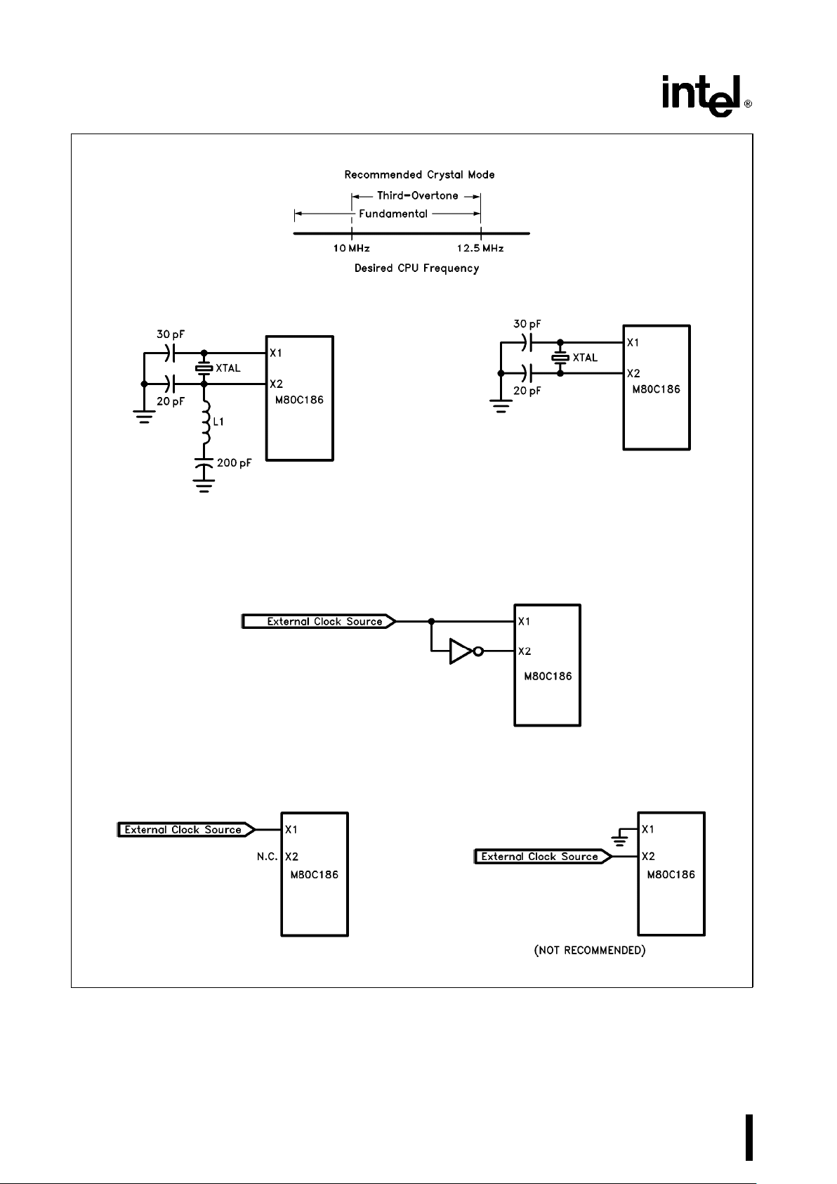
Oscillator
The M80C186 oscillator circuit is designed to be
used with either a parallel resonant fundamental or
third-overtone mode crystal, depending upon the
frequency range of the application as shown in Figure 8a. This is used as the time base for the
M80C186. The crystal frequency chosen should be
twice the required processor frequency. Use of an
LC or RC circuit is not recommended.
The oscillator output is not directly available external
to the M80C186. The two recommended crys-
tal configurations are shown in Figures 8b and 8c.
When used in third-overtone mode the tank circuit
shown in Figure 8b is recommended for stable operation. The sum of the stray capacitances and loading capacitors should equal the values shown. It is
advisable to limit stray capacitance between the X1
and X2 pins to less than 10 pF. While a fundamental-mode circuit will require approximately 1 ms for
start-up, the third-overtone arrangement may require
1 ms to 3 ms to stabilize.
Alternately the oscillator pins may be driven from an
external source as shown in Figure 8d or Figure 8e.
The configuration shown in Figure 8f is not recommended.
The following parameters may be used for choosing
a crystal:
Temperature Range:
b
55§Ctoa125§C
ESR (Equivalent Series Resistance): 40X max
C
0
(Shunt Capacitance of Crystal): 7.0 pf max
C
1
(Load Capacitance): 20 pFg2pF
Drive Level: 1 mW max
Clock Generator
The M80C186 clock generator provides the 50%
duty cycle processor clock for the M80C186. It does
this by dividing the oscillator output by 2 forming the
symmetrical clock. If an external oscillator is used,
the state of the clock generator will change on the
falling edge of the oscillator signal. The CLKOUT pin
provides the processor clock signal for use outside
the M80C186. This may be used to drive other system components. All timings are referenced to the
output clock.
READY Synchronization
The M80C186 provides both synchronous and asynchronous ready inputs. Asynchronous ready synchronization is accomplished by circuitry which samples ARDY in the middle of T
2,T3
and again in the
middle of each T
W
until ARDY is sampled HIGH.
One-half CLKOUT cycle of resolution time is used.
Full synchronization is performed only on the rising
edge of ARDY, i.e., the falling edge of ARDY must
be synchronized to the CLKOUT signal if it will occur
during T
2,T3
,orTW. High-to-LOW transitions of
ARDY must be performed synchronously to the CPU
clock.
A second ready input (SRDY) is provided to interface with externally synchronized ready signals. This
input is sampled at the end of T
2,T3
and again at
the end of each T
W
until it is sampled HIGH. By
using this input rather than the asynchronous ready
input, the half-clock cycle resolution time penalty is
eliminated.
17
Page 18
M80C186
270500–8
(8a)
270500–25
(8b)
(8c)
270500–24
Note 1:
XTAL Frequency L1 Value
20 Mhz 12.0 mH
g
20%
25 Mhz 8.2 mH
g
20%
(8d)
270500–26
(8e)
270500–27
(8f)
270500–28
Figure 8. M80C186 Oscillator Configurations
18
Page 19

M80C186
This input must satisfy set-up and hold times to guarantee proper operation of the circuit.
In addition, the M80C186, as part of the integrated
chip-select logic, has the capability to program WAIT
states for memory and peripheral blocks. This is discussed in the Chip Select/Ready Logic description.
RESET Logic
The M80C186 provides both a RES input pin and a
synchronized RESET pin for use with other system
components. The RES
input pin on the M80C186 is
provided with hysteresis in order to facilitate poweron Reset generation via an RC network. RESET is
guaranteed to remain active for at least five clocks
given a RES input of at least six clocks. RESET may
be delayed up to two and one-half clocks behind
RES
.
Multiple M80C186 processors may be synchronized
through the RES
input pin, since this input resets
both the processor and divide-by-two internal counter in the clock generator. In order to insure that the
divide-by-two counters all begin counting at the
same time, the active going edge of RES
must satisfy a 25 ns setup time before the falling edge of the
M80C186 clock input. In addition, in order to insure
that all CPUs begin executing in the same clock cycle, the reset must satisfy a 15 ns setup time before
the rising edge of the CLKOUT signal of all the processors.
LOCAL BUS CONTROLLER
The M80C186 provides a local bus controller to generate the local bus control signals. In addition, it employs a HOLD/HLDA protocol for relinquishing the
local bus to other bus masters. It also provides control lines that can be used to enable external buffers
and to direct the flow of data on and off the local
bus.
Memory/Peripheral Control
The M80C186 provides ALE, RD, and WR bus control signals. The RD
and WR signals are used to
strobe data from memory to the M80C186 or to
strobe data from the M80C186 to memory. The ALE
line provides a strobe to address latches for the multiplexed address/data bus. The M80C186 local bus
controller does not provide a memory/I/O
signal. If
this is required, the user will have to use the S2
signal (which will require external latching), make the
memory and I/O spaces nonoverlapping, or use only
the integrated chip-select circuitry.
Transceiver Control
The M80C186 generates two control signals to be
connected to external transceiver chips. This capability allows the addition of transceivers for extra
buffering without adding external logic. These control lines, DT/R
and DEN, are generated to control
the flow of data through the transceivers. The operation of these signals is shown in Table 6.
Table 6. Transceiver Control Signals Description
Pin Name Function
DEN (Data Enable) Enables the output
drivers of the
transceivers. It is active
LOW during memory,
I/O, or INTA cycles.
DT/R
(Data Transmit/ Determines the direction
Receive) of travel through the
transceivers. A HIGH
level directs data away
from the processor
during write operations,
while a LOW level directs
data toward the
processor during a read
operation.
Local Bus Arbitration
The M80C186 uses a HOLD/HLDA system of local
bus exchange. This provides an asynchronous bus
exchange mechanism. This means multiple masters
utilizing the same bus can operate at separate clock
frequencies. The M80C186 provides a single HOLD/
HLDA pair through which all other bus masters may
gain control of the local bus. This requires external
circuitry to arbitrate which external device will gain
control of the bus from the M80C186 when there is
more than one alternate local bus master. When the
M80C186 relinquishes control of the local bus, it
floats DEN
,RD,WR,S0–S2, LOCK, AD0–AD15,
A16– A19, BHE
, and DT/R to allow another master
to drive these lines directly.
The M80C186 HOLD latency time, i.e., the time between HOLD request and HOLD acknowledge, is a
function of the activity occurring in the processor
when the HOLD request is received. A HOLD request is the highest-priority activity request which
the processor may receive: higher than instruction
fetching or internal DMA cycles. However, if a DMA
cycle is in progress, the M80C186 will complete the
transfer before relinquishing the bus. This implies
that if a HOLD request is received just as a DMA
transfer begins, the HOLD latency time can be as
great as 4 bus cycles. This will occur if a DMA word
transfer operation is taking place from an odd ad-
19
Page 20

M80C186
dress to an odd address. This is a total of 16 clocks
or more, if WAIT states are required. In addition, if
locked transfers are performed, the HOLD latency
time will be increased by the length of the locked
transfer.
Local Bus Controller and Reset
Upon receipt of a RESET pulse from the RES input,
the local bus controller will perform the following action:
#
Drive DEN,RD, and WR HIGH for one clock cycle, then float.
NOTE:
RD
is also provided with an internal pull-up device
to prevent the processor from inadvertently entering Queue Status mode during reset.
#
Drive S0 –S2 to the passive state (all HIGH) and
then float.
#
Drive LOCK HIGH and then float.
#
Float AD0 – 15, A16–19, BHE, DT/R.
#
Drive ALE LOW (ALE is never floated).
#
Drive HLDA LOW.
INTERNAL PERIPHERAL INTERFACE
All the M80C186 integrated peripherals are controlled via 16-bit registers contained within an internal 256-byte control block. This control block may
be mapped into either memory or I/O space. Internal
logic will recognize the address and respond to the
bus cycle. During bus cycles to internal registers, the
bus controller will signal the operation externally
(i.e., the RD
,WR, status, address, data, etc., lines
will be driven as in a normal bus cycle), but D
15–0
,
SRDY, and ARDY will be ignored. The base address
of the control block must be on an even 256-byte
boundary (i.e., the lower 8 bits of the base address
are all zeros). All of the defined registers within this
control block may be read or written by the
M80C186 CPU at any time. The location of any register contained within the 256-byte control block is
determined by the current base address of the control block.
The control block base address is programmed via a
16-bit relocation register contained within the control
block at offset FEH from the base address of the
control block (see Figure 9). It provides the upper 12
bits of the base address of the control block. The
control block is effectively an internal chip select
range and must abide by all the rules concerning
chip selects (the chip select circuitry is discussed
later in this data sheet). Any access to the 256 bytes
of the control block activates an internal chip select.
Other chip selects may overlap the control block
only if they are programmed to zero wait states and
ignore external ready. In addition, bit 12 of this register determines whether the control block will be
mapped into I/O or memory space. If this bit is 1, the
control block will be located in memory space,
whereas if the bit is 0, the control block will be located in I/O space. If the control register block is
mapped into I/O space, the upper 4 bits of the base
address must be programmed as 0 (since I/O addresses are only 16 bits wide).
In addition to providing relocation information for the
control block, the relocation register contains bits
which place the interrupt controller into slave mode,
and cause the CPU to interrupt upon encountering
ESC instructions. At RESET, the relocation register
is set to 20FFH. This causes the control block to
start at FF00H in I/O space. An offset map of the
256-byte control register block is shown in Figure
10.
The integrated M80C186 peripherals operate semiautonomously from the CPU. Access to them for the
most part is via software read/write of the control
block. Most of these registers can be both read and
written. A few dedicated lines, such as interrupts and
DMA request provide real-time communication between the CPU and peripherals as in a more conventional system utilizing discrete peripheral blocks.
The overall interaction and function of the peripheral
blocks has not substantially changed.
CHIP-SELECT/READY GENERATION
LOGIC
The M80C186 contains logic which provides
programmable chip-select generation for both
memories and peripherals. In addition, it can be programmed to provide READY (or WAIT state) generation. It can also povide latched address bits A1 and
A2. The chip-select lines are active for all memory
and I/O cycles in their programmed areas, whether
they be generated by the CPU or by the integrated
DMA unit.
Memory Chip Selects
The M80C186 provides 6 memory chip select outputs for 3 address areas; upper memory, lower
memory, and midrange memory. One each is provided for upper memory and lower memory, while four
are provided for midrange memory.
The range for each chip select is user-programmable and can be set to 2K, 4K, 8K, 16K, 32K, 64K,
128K (plus 1K and 256K for upper and lower chip
selects). In addition, the beginning or base address
20
Page 21

M80C186
15 14 131211109876543210
OFFSET: FEH ET SLAVE/MASTER X M/IO Relocation Address Bits R19 – R8
ET
e
ESC Trap / No ESC Trap (1/0)
M/IO
e
Register block located in Memory / I/O Space (1/0)
SLAVE/MASTER
e
Configures interrupt controller for Slave/Master Mode (1/0)
Figure 9. Relocation Register
OFFSET
Relocation Register FEH
DMA Descriptors Channel 1
DAH
D0H
DMA Descriptors Channel 0
CAH
C0H
Chip-Select Control Registers
A8H
A0H
Time 2 Control Registers
66H
60H
Time 1 Control Registers
5EH
58H
Time 0 Control Registers
56H
50H
Interrupt Controller Registers
3EH
20H
Figure 10. Internal Register Map
of the midrange memory chip select may also be
selected. Only one chip select may be programmed
to be active for any memory location at a time.
M80C186 memory is arranged in words but chip selects are sized in bytes. If sixteen 64K x 1 memories
are used then the memory block size will be 128K,
not 64K.
Upper Memory CS
The M80C186 provides a chip select, called UCS,
for the top of memory. The top of memory is usually
used as the system memory because after reset the
M80C186 begins executing at memory location
FFFF0H.
The upper limit of memory defined by this chip select
is always FFFFFH, while the lower limit is programmable. By programming the lower limit, the size of
the select block is also defined. Table 7 shows the
relationship between the base address selected and
the size of the memory block obtained.
Table 7. UMCS Programming Values
Starting
Memory UMCS Value
Address
Block (Assuming
(Base
Size R0
eR1eR2e
0)
Address)
FFC00 1K FFF8H
FF800 2K FFB8H
FF000 4K FF38H
FE000 8K FE38H
FC000 16K FC38H
F8000 32K F838H
F0000 64K F038H
E0000 128K E038H
C0000 256K C038H
The lower limit of this memory block is defined in the
UMCS register (see Figure 11). This register is at
offset A0H in the internal control block. The legal
values for bits 6 –13 and the resulting starting address and memory block sizes are given in Table 7.
Any combination of bits 6– 13 not shown in Table 7
will result in undefined operation. After reset, the
UMCS register is programmed for a 1K area. It must
be reprogrammed if a larger upper memory area is
desired.
Any internally generated 20-bit address whose upper 16 bits are greater than or equal to UMCS (with
bits 0–5 ‘‘0’’) will cause UCS to be activated. UMCS
bits R2 –R0 are used to specify READY mode for the
area of memory defined by this chip-select register,
as explained below.
Lower Memory CS
The M80C186 provides a chip select for low memory
called LCS
. The bottom of memory contains the in-
terrupt vector table, starting at location 00000H.
21
Page 22

M80C186
The lower limit of memory defined by this chip select
is always 0H, while the upper limit is programmable.
By programming the upper limit, the size of the
memory block is also defined. Table 8 shows the
relationship between the upper address selected
and the size of the memory block obtained.
Table 8. LMCS Programming Values
Upper
Memory LMCS Value
Address
Block (Assuming
Size R0
eR1eR2e
0)
003FFH 1K 0038H
007FFH 2K 0078H
00FFFH 4K 00F8H
01FFFH 8K 01F8H
03FFFH 16K 03F8H
07FFFH 32K 07F8H
0FFFFH 64K 0FF8H
1FFFFH 128K 1FF8H
3FFFFH 256K 3FF8H
The upper limit of this memory block is defined in the
LMCS register (see Figure 12). This register is at
offset A2H in the internal control block. The legal
values for bits 6 – 15 and the resulting upper address
and memory block sizes are given in Table 8. Any
combination of bits 6– 15 not shown in Table 8 will
result in undefined operation. After reset, the LMCS
register value is undefined. However, the LCS
chipselect line will not become active until the LMCS
register is accessed.
Any internally generated 20-bit address whose upper 16 bits are less than or equal to LMCS (with bits
0– 5 ‘‘1’’) will cause LCS
to be active. LMCS register
bits R2 –R0 are used to specify the READY mode for
the area of memory defined by this chip-select register.
Mid-Range Memory CS
The M80C186 provides four MCS lines which are
active within a user-locatable memory block. This
block can be located within the M80C186 1M byte
memory address space exclusive of the areas defined by UCS and LCS. Both the base ad-
dress and size of this memory block are programmable.
The size of the memory block defined by the midrange select lines, as shown in Table 9, is determined by bits 8–14 of the MPCS register (see Figure
13). This register is at location A8H in the internal
control block. One and only one of bits 8 –14 must
be set at a time. Unpredictable operation of the MCS
lines will otherwise occur. Each of the four chip-select lines is active for one of the four equal contiguous divisions of the mid-range block. Thus, if the total block size is 32K, each chip select is active for 8K
of memory with MCS0 being active for the first range
and MCS3
being active for the last range.
The EX and MS in MPCS relate to peripheral functionally as described in a later section.
Table 9. MPCS Programming Values
Total Block Individual MPCS Bits
Size Select Size 14 –8
8K 2K 0000001B
16K 4K 0000010B
32K 8K 0000100B
64K 16K 0001000B
128K 32K 0010000B
256K 64K 0100000B
512K 128K 1000000B
The base address of the mid-range memory block is
defined by bits 15– 9 of the MMCS register (see Figure 14). This register is at offset A6H in the internal
control block. These bits correspond to bits
A19– A13 of the 20-bit memory address. Bits
A12– A0 of the base address are always 0. The base
address may be set at any integer multiple of the
size of the total memory block selected. For example, if the mid-range block size is 32K (or the size of
the block for which each MCS
line is active is 8K),
the block could be located at 10000H or 18000H,
but not at 14000H, since the first few integer multiples of a 32K memory block are 0H, 8000H,
10000H, 18000H, etc. After reset, the contents of
both of these registers is undefined. However, none
of the MCS
lines will be active until both the MMCS
and MPCS registers are accessed.
1514131211109876543210
OFFSET: A0H 1 1 UUUUUUUU1 1 1R2R1R0
A19 A11
Figure 11. UMCS Register
1514131211109876543210
OFFSET: A2H 0 0 UUUUUUUU1 1 1R2R1R0
A19 A11
Figure 12. LMCS Register
22
Page 23

M80C186
1514131211109876543210
OFFSET: A8H 1 M6 M5 M4 M3 M2 M1 M0 EX MS 1 1 1 R2 R1 R0
Figure 13. MPCS Register
15 9 3 0
OFFSET: A6H UUUUUUU111111R2R1R0
A19 A13
Figure 14. MMCS Register
MMCS bits R2–R0 specify READY mode of operation for all mid-range chip selects. All devices in midrange memory must use the same number of WAIT
states.
The 512K block size for the mid-range memory chip
selects is a special case. When using 512K, the
base address would have to be at either locations
00000H or 80000H. If it were to be programmed at
00000H when the LCS
line was programmed, there
would be an internal conflict between the LCS
ready
generation logic and the MCS
ready generation logic. Likewise, if the base address were programmed
at 80000H, there would be a conflict with the UCS
ready generation logic. Since the LCS chip-select
line does not become active until programmed, while
the UCS
line is active at reset, the memory base can
be set only at 00000H. If this base address is selected, however, the LCS
range must not be pro-
grammed.
Peripheral Chip Selects
The M80C186 can generate chip selects for up to
seven peripheral devices. These chip selects are active for seven contiguous blocks of 128 bytes above
a programmable base address. This base address
may be located in either memory or I/O space.
Seven CS
lines called PCS0 – 6 are generated by the
M80C186. The base address is user-programmable;
however it can only be a multiple of 1K bytes, i.e.,
the least significant 10 bits of the starting address
are always 0.
PCS5
and PCS6 can also be programmed to provide
latched address bits A1, A2. If so programmed, they
cannot be used as peripheral selects. These outputs
can be connected directly to the A0, A1 pins used
for selecting internal registers of 8-bit peripheral
chips. This scheme simplifies the hardware interface
because the 8-bit registers of peripherals are simply
treated as 16-bit registers located on even boundaries in I/O space or memory space where only the
lower 8-bits of the register are significant: the upper
8-bits are ‘‘don’t cares.’’
The starting address of the peripheral chip-select
block is defined by the PACS register (see Figure
15). This register is located at offset A4H in the internal control block. Bits 15– 6 of this register correspond to bits 19 – 10 of the 20-bit Programmable
Base Address (PBA) of the peripheral chip-select
block. Bits 9 –0 of the PBA of the peripheral chip-select block are all zeros. If the chip-select block is
located in I/O space, bits 12– 15 must be programmed zero, since the I/O address is only 16 bits
wide. Table 10 shows the address range of each
peripheral chip select with respect to the PBA contained in PACS register.
15 6 5 3 0
OFFSET: A4H UUUUUUUUUU1 11R2R1R0
A19 A10
Figure 15. PACS Register
23
Page 24

M80C186
The user should program bits 15 – 6 to correspond to
the desired peripheral base location. PACS bits 0 –2
are used to specify READY mode for PCS0
–PCS3.
Table 10. PCS Address Ranges
PCS Line Active between Locations
PCS0 PBA ÐPBAa127
PCS1 PBA
a
128ÐPBAa255
PCS2 PBA
a
256ÐPBAa383
PCS3 PBA
a
384ÐPBAa511
PCS4 PBA
a
512ÐPBAa639
PCS5 PBAa640ÐPBAa767
PCS6 PBA
a
768ÐPBAa895
The mode of operation of the peripheral chip selects
is defined by the MPCS register (which is also used
to set the size of the mid-range memory chip-select
block, see Figure 13). This register is located at offset A8H in the internal control block. Bit 7 is used to
select the function of PCS5
and PCS6, while bit 6 is
used to select whether the peripheral chip selects
are mapped into memory or I/O space. Table 11
describes the programming of these bits. After reset,
the contents of both the MPCS and the PACS registers are undefined, however none of the PCS lines
will be active until both of the MPCS and PACS registers are accessed.
Table 11. MS, EX Programming Values
Bit Description
MS 1ePeripherals mapped into memory space.
0
e
Peripherals mapped into I/O space.
EX 0
e
5 PCS lines. A1, A2 provided.
1
e
7 PCS lines. A1, A2 are not provided.
MPCS bits 0– 2 are used to specify READY mode for
PCS4
–PCS6 as outlined below.
READY Generation Logic
The M80C186 can generate a ‘‘READY’’ signal internally for each of the memory or peripheral CS
lines. The number of WAIT states to be inserted for
each peripheral or memory is programmable to provide 0– 3 wait states for all accesses to the area for
which the chip select is active. In addition, the
M80C186 may be programmed to either ignore external READY for each chip-select range individually
or to factor external READY with the integrated
ready generator.
READY control consists of 3 bits for each CS
line or
group of lines generated by the M80C186. The interpretation of the ready bits is shown in Table 12.
Table 12. READY Bits Programming
R2 R1 R0 Number of WAIT States Generated
0 0 0 0 wait states, external RDY
also used.
0 0 1 1 wait state inserted, external RDY
also used.
0 1 0 2 wait states inserted, external RDY
also used.
0 1 1 3 wait states inserted, external RDY
also used.
1 0 0 0 wait states, external RDY
ignored.
1 0 1 1 wait state inserted, external RDY
ignored.
1 1 0 2 wait states inserted, external RDY
ignored.
1 1 1 3 wait states inserted, external RDY
ignored.
The internal ready generator operates in parallel
with external READY, not in series if the external
READY is used (R2
e
0). This means, for example,
if the internal generator is set to insert two wait
states, but activity on the external READY lines will
insert four wait states, the processor will only insert
four wait states, not six. This is because the two wait
states generated by the internal generator overlapped the first two wait states generated by the external ready signal. Note that the external ARDY and
SRDY lines are always ignored during cycles accessing internal peripherals.
R2– R0 of each control word specifies the READY
mode for the corresponding block, with the exception of the peripheral chip selects: R2–R0 of PACS
set the PCS0
–3 READY mode, R2 – R0 of MPCS set
the PCS4
–6 READY mode.
Chip Select/Ready Logic and Reset
Upon reset, the Chip-Select/Ready Logic will perform the following actions:
#
All chip-select outputs will be driven HIGH.
#
Upon leaving RESET, the UCS line will be programmed to provide chip selects to a 1K block
with the accompanying READY control bits set at
011 to allow the maximum number of internal wait
states in conjunction with external Ready consideration (i.e., UMCS resets to FFFBH).
#
No other chip select or READY control registers
have any predefined values after RESET. They
will not become active until the CPU accesses
their control registers. Both the PACS and MPCS
registers must be accessed before the PCS
lines
will become active.
24
Page 25

M80C186
DMA CHANNELS
The M80C186 DMA controller provides two independent high-speed DMA channels. Data transfers can
occur between memory and I/O spaces (e.g., Memory to I/O) or within the same space (e.g., Memory
to Memory or I/O to I/O). Data can be transferred
either in bytes (8 bits) or in words (16 bits) to or from
even or odd addresses. Each DMA channel maintains both a 20-bit source and destination pointer
which can be optionally incremented or decremented after each data transfer (by one or two depending
on byte or word transfers). Each data transfer consumes 2 bus cycles (a minimum of 8 clocks), one
cycle to fetch data and the other to store data.
DMA Operation
Each channel has six registers in the control block
which define each channel’s specific operation. The
control registers consist of a 20-bit Source pointer (2
words), a 20-bit destination pointer (2 words), a 16bit Transfer Counter, and a 16-bit Control Word. The
format of the DMA Control Blocks is shown in Table
13. The Transfer Count Register (TC) specifies the
number of DMA transfers to be performed. Up to
64K byte or word transfers can be performed with
automatic termination. The Control Word defines the
channel’s operation (see Figure 17). All registers
may be modified or altered during any DMA activity.
Any changes made to these registers will be reflected immediately in DMA operation.
Table 13. DMA Control Block Format
Register Name
Register Address
Ch. 0 Ch. 1
Control Word CAH DAH
Transfer Count C8H D8H
Destination Pointer (upper 4 C6H D6H
bits)
Destination Pointer C4H D4H
Source Pointer (upper 4 bits) C2H D2H
Source Pointer C0H D0H
270500–9
Figure 16. DMA Unit Block Diagram
25
Page 26

M80C186
1514131211109876543 2 10
T
D
M/ DESTINATION M/ SOURCE
TC INT SYN P
R
X
CHG/ ST/ B
/
IO
DEC INC IO DEC INC Q NOCHG STOP W
XeDON’T CARE.
Figure 17. DMA Control Register
DMA Channel Control Word Register
Each DMA Channel Control Word determines the
mode of operation for the particular M80C186 DMA
channel. This register specifies:
#
the mode of synchronization;
#
whether bytes or words will be transferred;
#
whether interrupts will be generated after the last
transfer;
#
whether DMA activity will cease after a programmed number of DMA cycles;
#
the relative priority of the DMA channel with respect to the other DMA channel;
#
whether the source pointer will be incremented,
decremented, or maintained constant after each
transfer;
#
whether the source pointer addresses memory or
I/O space;
#
whether the destination pointer will be incremented, decremented, or maintained constant after
each transfer; and
#
whether the destination pointer will address
memory or I/O space.
The DMA channel control registers may be changed
while the channel is operating. However, any changes made during operation will affect the current DMA
transfer.
DMA Control Word Bit Descriptions
B/W: Byte/Word (0/1) Transfers.
ST/STOP
: Start/stop (1/0) Channel.
CHG/NOCHG: Change/Do not change (1/0)
ST/STOP
bit. If this bit is set when
writing to the control word, the
ST/STOP
bit will be programmed
by the write to the control word. If
this bit is cleared when writing the
control word, the ST/STOP
bit will
not be altered. This bit is not
stored; it will always be a 0 on
read.
INT: Enable Interrupts to CPU on
Transfer Count termination.
TC: If set, DMA will terminate when
the contents of the Transfer Count
register reach zero. The ST/STOP
bit will also be reset at this point if
TC is set. If this bit is cleared, the
DMA unit will decrement the transfer count register for each DMA
cycle, but the DMA transfer will
not stop when the contents of the
TC register reach zero.
SYN 00 No synchronization.
NOTE:
When unsynchronized transfers
are specified, the TC bit will be ignored and the ST bit will be
cleared upon the transfer count
reaching zero, stopping the channel.
(2 bits) 01 Source synchronization.
10 Destination synchronization.
11 Unused.
SOURCE:INC Increment source pointer by 1 or 2
(depends on B
/W) after each
transfer.
M/IO
Source pointer is in M/IO space
(1/0).
DEC Decrement source pointer by 1 or
2 (depends on B
/W) after each
transfer.
DEST: INC Increment destination pointer by 1
or 2 (B
/W) after each transfer.
M/IO Destination pointer is in M/IO
space (1/0).
DEC Decrement destination pointer by
1 or 2 (depending on B
/W) after
each transfer.
P Channel priorityÐrelative to other
channel.
0 low priority.
1 high priority.
Channels will alternate cycles if
both set at same priority level.
TDRQ 0: Disable DMA requests from tim-
er 2.
1: Enable DMA requests from tim-
er 2.
Bit 3 Bit 3 is not used.
26
Page 27

M80C186
If both INC and DEC are specified for the same
pointer, the pointer will remain constant after each
cycle.
DMA Destination and Source Pointer
Registers
Each DMA channel maintains a 20-bit source and a
20-bit destination pointer. Each of these pointers
takes up two full 16-bit registers in the peripheral
control block. The lower four bits of the upper register contain the upper four bits of the 20-bit physical
address (see Figure 18). These pointers may be individually incremented or decremented after each
transfer. If word transfers are performed the pointer
is incremented or decremented by two. Each pointer
may point into either memory or I/O space. Since
the DMA channels can perform transfers to or from
odd addresses, there is no restriction on values for
the pointer registers. Higher transfer rates can be
obtained if all word transfers are performed to even
addresses, since this will allow data to be accessed
in a single memory access.
DMA Transfer Count Register
Each DMA channel maintains a 16-bit transfer count
register (TC). This register is decremented after every DMA cycle, regardless of the state of the TC bit
in the DMA Control Register. If the TC bit in the DMA
control word is set or if unsynchronized transfers are
programmed, however, DMA activity will terminate
when the transfer count register reaches zero.
DMA Requests
Data transfers may be either source or destination
synchronized, that is either the source of the data or
the destination of the data may request the data
transfer. In addition, DMA transfers may be unsynchronized; that is, the transfer will take place continually until the correct number of transfers has occurred. When source or unsynchronized transfers
are performed, the DMA channel may begin another
transfer immediately after the end of a previous
DMA transfer. This allows a complete transfer to
take place every 2 bus cycles or eight clock cycles
(assuming no wait states). No prefetching occurs
when destination synchronization is performed, however. Data will not be fetched from the source address until the destination device signals that it is
ready to receive it. When destination synchronized
transfers are requested, the DMA controller will relinquish control of the bus after every transfer. If no
other bus activity is initiated, another DMA cycle will
begin after two processor clocks. This is done to
allow the destination device time to remove its request if another transfer is not desired. Since the
DMA controller will relinquish the bus, the CPU can
initiate a bus cycle. As a result, a complete bus cycle
will often be inserted between destination synchronized transfers. These lead to the maximum DMA
transfer rates shown in Table 14.
Table 14. Maximum DMA
Transfer Rates
Type of
Synchronization CPU Running CPU Halted
Selected
Unsynchronized 2.5MBytes/sec 2.5MBytes/sec
Source Synch 2.5MBytes/sec 2.5MBytes/sec
Destination Synch 1.7MBytes/sec 2.0MBytes/sec
HIGHER
REGISTER XXX XXX XXX A19 – A16
ADDRESS
LOWER
REGISTER A15–A12 A11 – A8 A7 – A4 A3 – A0
ADDRESS
15 0
XXX
e
DON’T CARE
Figure 18. DMA Memory Pointer Register Format
27
Page 28

M80C186
DMA Acknowledge
No explicit DMA acknowledge pulse is provided.
Since both source and destination pointers are
maintained, a read from a requesting source, or a
write to a requesting destination, should be used as
the DMA acknowledge signal. Since the chip-select
lines can be programmed to be active for a given
block of memory or I/O space, and the DMA pointers can be programmed to point to the same given
block, a chip-select line could be used to indicate a
DMA acknowledge.
DMA Priority
The DMA channels may be programmed such that
one channel is always given priority over the other,
or they may be programmed such as to alternate
cycles when both have DMA requests pending. DMA
cycles always have priority over internal CPU cycles
except between locked memory accesses or word
accesses to odd memory locations; however, an external bus hold takes priority over an internal DMA
cycle. Because an interrupt request cannot suspend
a DMA operation and the CPU cannot access memory during a DMA cycle, interrupt latency time will
suffer during sequences of continuous DMA cycles.
An NMI request, however, will cause all internal
DMA activity to halt. This allows the CPU to quickly
respond to the NMI request.
DMA Programming
DMA cycles will occur whenever the ST/STOP bit of
the Control Register is set. If synchronized transfers
are programmed, a DRQ must also have been generated. Therefore the source and destination transfer pointers, and the transfer count register (if used)
must be programmed before this bit is set.
Each DMA register may be modified while the channel is operating. If the CHG/NOCHG bit is cleared
when the control register is written, the ST/STOP bit
of the control register will not be modified by the
write. If multiple channel registers are modified, it is
recommended that a LOCKED string transfer be
used to prevent a DMA transfer from occurring between updates to the channel registers.
DMA Channels and Reset
Upon RESET, the DMA channels will perform the
following actions:
#
The Start/Stop bit for each channel will be reset
to STOP.
#
Any transfer in progress is aborted.
TIMERS
The M80C186 provides three internal 16-bit programmable timers (see Figure 19). Two of these are
highly flexible and are connected to four external
pins (2 per timer). They can be used to count external events, time external events, generate nonrepetitive waveforms, etc. The third timer is not connected to any external pins, and is useful for real-time
coding and time delay applications. In addition, this
third timer can be used as a prescaler to the other
two, or as a DMA request source.
270500–10
Figure 19. Timer Block Diagram
28
Page 29

M80C186
Timer Operation
The timers are controlled by 11 16-bit registers in
the internal peripheral control block. The configuration of these registers is shown in Table 15. The
count register contains the current value of the timer. It can be read or written at any time independent
of whether the timer is running or not. The value of
this register will be incremented for each timer
event. Each of the timers is equipped with a MAX
COUNT register, which defines the maximum count
the timer will reach. After reaching the MAX COUNT
register value, the timer count value will reset to zero
during that same clock, i.e., the maximum count value is never stored in the count register itself. Timers
0 and 1 are, in addition, equipped with a second
MAX COUNT register, which enables the timers to
alternate their count between two different MAX
COUNT values programmed by the user. If a single
MAX COUNT register is used, the timer output pin
will switch LOW for a single clock, 1 clock after the
maximum count value has been reached. In the dual
MAX COUNT register mode, the output pin will indicate which MAX COUNT register is currently in use,
thus allowing nearly complete freedom in selecting
waveform duty cycles. For the timers with two MAX
COUNT registers, the RIU bit in the control register
determines which is used for the comparison.
Each timer gets serviced every fourth CPU-clock cycle, and thus can operate at speeds up to one-quarter the internal clock frequency (one-eighth the crystal rate). External clocking of the timers may be done
at up to a rate of one-quarter of the internal CPUclock rate. Due to internal synchronization and pipelining of the timer circuitry, a timer output may take
up to 6 clocks to respond to any individual clock or
gate input.
Since the count registers and the maximum count
registers are all 16 bits wide, 16 bits of resolution are
provided. Any Read or Write access to the timers will
add one wait state to the minimum four-clock bus
cycle, however. This is needed to synchronize and
coordinate the internal data flows between the internal timers and the internal bus.
The timers have several programmable options.
#
All three timers can be set to halt or continue on
a terminal count.
#
Timers 0 and 1 can select between internal and
external clocks, alternate between MAX COUNT
registers and be set to retrigger on external
events.
#
The timers may be programmed to cause an interrupt on terminal count.
These options are selectable via the timer mode/
control word.
Timer Mode/Control Register
The mode/control register (see Figure 20) allows
the user to program the specific mode of operation
or check the current programmed status for any of
the three integrated timers.
Table 15. Timer Control Block Format
Register Name
Register Offset
Tmr. 0 Tmr. 1 Tmr. 2
Mode/Control Word 56H 5EH 66H
Max Count B 54H 5CH not present
Max Count A 52H 5AH 62H
Count Register 50H 58H 60H
15 14 13 12 11 5 4 3 2 1 0
EN INH INT RIU 0 . . . MC RTG P EXT ALT CONT
Figure 20. Timer Mode/Control Register
29
Page 30

M80C186
ALT:
The ALT bit determines which of two MAX COUNT
registers is used for count comparison. If ALT
e
0,
register A for that timer is always used, while if ALT
e
1, the comparison will alternate between register
A and register B when each maximum count is
reached. This alternation allows the user to change
one MAX COUNT register while the other is being
used, and thus provides a method of generating
non-repetitive waveforms. Square waves and pulse
outputs of any duty cycle are a subset of available
signals obtained by not changing the final count registers. The ALT bit also determines the function of
the timer output pin. If ALT is zero, the output pin will
go LOW for one clock, the clock after the maximum
count is reached. If ALT is one, the output pin will
reflect the current MAX COUNT register being used
(0/1 for B/A).
CONT:
Setting the CONT bit causes the associated timer to
run continuously, while resetting it causes the timer
to halt upon maximum count. If COUNT
e
0 and
ALT
e
1, the timer will count to the MAX COUNT
register A value, reset, count to the register B value,
reset, and halt.
EXT:
The external bit selects between internal and external clocking for the timer. The external signal may
be asynchronous with respect to the M80C186
clock. If this bit is set, the timer will count LOW-toHIGH transitions on the input pin. If cleared, it will
count an internal clock while using the input pin for
control. In this mode, the function of the external pin
is defined by the RTG bit. The maximum input to
output transition latency time may be as much as 6
clocks. However, clock inputs may be pipelined as
closely together as every 4 clocks without losing
clock pulses.
P:
The prescaler bit is ignored unless internal clocking
has been selected (EXT
e
0). If the P bit is a zero,
the timer will count at one-fourth the internal CPU
clock rate. If the P bit is a one, the output of timer 2
will be used as a clock for the timer. Note that the
user must initialize and start timer 2 to obtain the
prescaled clock.
RTG:
Retrigger bit is only active for internal clocking (EXT
e
0). In this case it determines the control function
provided by the input pin.
If RTG
e
0, the input level gates the internal clock
on and off. If the input pin is HIGH, the timer will
count; if the input pin is LOW, the timer will hold its
value. As indicated previously, the input signal may
be asynchronous with respect to the M80C186
clock.
When RTG
e
1, the input pin detects LOW-to-HIGH
transitions. The first such transition starts the timer
running, clearing the timer value to zero on the first
clock, and then incrementing thereafter. Further
transitions on the input pin will again reset the timer
to zero, from which it will start counting up again. If
CONT
e
0, when the timer has reached maximum
count, the EN bit will be cleared, inhibiting further
timer activity.
EN:
The enable bit provides programmer control over
the timer’s RUN/HALT status. When set, the timer is
enabled to increment subject to the input pin constraints in the internal clock mode (discussed previously). When cleared, the timer will be inhibited from
counting. All input pin transistions during the time EN
is zero will be ignored. If CONT is zero, the EN bit is
automatically cleared upon maximum count.
INH
:
The inhibit bit allows for selective updating of the
enable (EN) bit. If INH
is a one during the write to the
mode/control word, then the state of the EN bit will
be modified by the write. If INH
is a zero during the
write, the EN bit will be unaffected by the operation.
This bit is not stored; it will always bea0onaread.
INT:
When set, the INT bit enables interrupts from the
timer, which will be generated on every terminal
count. If the timer is configured in dual MAX COUNT
register mode, an interrupt will be generated each
time the value in MAX COUNT register A is reached,
and each time the value in MAX COUNT register B is
reached. If this enable bit is cleared after the interrupt request has been generated, but before a pending interrupt is serviced, the interrupt request will still
be in force. (The request is latched in the Interrupt
Controller).
MC:
The Maximum Count bit is set whenever the timer
reaches its final maximum count value. If the timer is
configured in dual MAX COUNT register mode, this
bit will be set each time the value in MAX COUNT
register A is reached, and each time the value in
MAX COUNT register B is reached. This bit is set
30
Page 31

M80C186
regardless of the timer’s interrupt-enable bit. The
MC bit gives the user the ability to monitor timer
status through software instead of through interrupts.
Programmer intervention is required to clear this bit.
RIU:
The Register In Use bit indicates which MAX
COUNT register is currently being used for comparison to the timer count value. A zero value indicates
register A. The RIU bit cannot be written, i.e., its
value is not affected when the control register is written. It is always cleared when the ALT bit is zero.
Not all mode bits are provided for timer 2. Certain
bits are hardwired as indicated below:
ALTe0, EXTe0, Pe0, RTGe0, RIUe0
Count Registers
Each of the three timers has a 16-bit count register.
The current contents of this register may be read or
written by the processor at any time. If the register is
written into while the timer is counting,the new value
will take effect in the current count cycle.
Max Count Registers
Timers 0 and 1 have two MAX COUNT registers,
while timer 2 has a single MAX COUNT register.
These contain the number of events the timer will
count. In timers 0 and 1, the MAX COUNT register
used can alternate between the two max count values whenever the current maximum count is
reached. The condition which causes a timer to reset is equivalent between the current count value
and the max count being used. This means that if
the count is changed to be above the max count
value, or if the max count value is changed to be
below the current value, the timer will not reset to
zero, but rather will count to its maximum value,
‘‘wrap around’’ to zero, then count until the max
count is reached.
Timers and Reset
Upon RESET, the Timers will perform the following
actions:
#
All EN (Enable) bits are reset preventing timer
counting.
#
All SEL (Select) bits are reset to zero. This selects MAX COUNT register A, resulting in the
Timer Out pins going HIGH upon RESET.
INTERRUPT CONTROLLER
The M80C186 can receive interrupts from a number
of sources, both internal and external. The internal
interrupt controller serves to merge these requests
on a priority basis, for individual service by the CPU.
Internal interrupt sources (Timers and DMA channels) can be disabled by their own control registers
or by mask bits within the interrupt controller. The
M80C186 interrupt controller has its own control
register that set the mode of operation for the controller.
The interrupt controller will resolve priority among
requests that are pending simultaneously. Nesting is
provided so interrupt service routines for lower priority interrupts may themselves be interrupted by higher priority interrupts. A block diagram of the interrupt
controller is shown in Figure 21.
The M80C186 has a special slave mode in which the
internal interrupt controller acts as a slave to an external master. The controller is programmed into this
mode by setting bit 14 in the peripheral control block
relocation register. (See Slave Mode section.)
MASTER MODE OPERATION
Interrupt Controller External Interface
For external interrupt sources, five dedicated pins
are provided. One of these pins is dedicated to NMI,
non-maskable interrupt. This is typically used for
power-fail interrupts, etc. The other four pins may
function either as four interrupt input lines with internally generated interrupt vectors, as an interrupt line
and an interrupt acknowledge line (called the ‘‘cascade mode’’) along with two other input lines with
internally generated interrupt vectors, or as two interrupt input lines and two dedicated interrupt acknowledge output lines. When the interrupt lines are
configured in cascade mode, the M80C186 interrupt
controller will not generate internal interrupt vectors.
External sources in the cascade mode use externally generated interrupt vectors. When an interrupt is
acknowledged, two INTA
cycles are initiated and the
vector is read into the M80C186 on the second cycle. The capability to interface to external M82C59A
programmable interrupt controllers is thus provided
when the inputs are configured in cascade mode.
31
Page 32

M80C186
Interrupt Controller Modes of
Operation
The basic modes of operation of the interrupt controller in master mode are similar to the M82C59A.
The interrupt controller responds indentically to internal interrupts in all three modes: the difference is
only in the interpretation of function of the four external interrupt pins. The interrupt controller is set into
one of these three modes by programming the correct bits in the INT0 and INT1 control registers. The
modes of interrupt controller operation are as follows:
Fully Nested Mode
When in the fully nested mode four pins are used as
direct interrupt requests as in Figure 22. The vectors
for these four inputs are generated internally. An inservice bit is provided for every interrupt source. If a
lower-priority device requests an interrupt while the
in service bit (IS) is set, no interrupt will be generated by the interrupt controller. In addition, if another
interrupt request occurs from the same interrupt
source while the in-service bit is set, no interrupt will
be generated by the interrupt controller. This allows
interrupt service routines to operate with interrupts
enabled without being themselves interrupted by
lower-priority interrupts. Since interrupts are enabled, higher-priority interrupts will be serviced.
When a service routine is completed, the proper IS
bit must be reset by writing the proper pattern to the
EOI register. This is required to allow subsequent
interrupts from this interrupt source and to allow
servicing of lower-priority interrupts. An EOI com-
mand is issued at the end of the service routine just
before the issuance of the return from interrupt instruction. If the fully nested structure has been upheld, the next highest-priority source with its IS bit
set is then serviced.
Cascade Mode
The M80C186 has four interrupt pins and two of
them have dual functions. In the fully nested mode
the four pins are used as direct interrupt inputs and
the corresponding vectors are generated internally.
In the cascade mode, the four pins are configured
into interrupt input-dedicated acknowledge signal
pairs. The interconnection is shown in Figure 23.
INT0 is an interrupt input interfaced to an M82C59A,
while INT2/INTA0
serves as the dedicated interrupt
acknowledge signal to that peripheral. The same is
true for INT1 and INT3/INTA1
. Each pair can selectively be placed in the cascade or non-cascade
mode by programming the proper value into INT0
and INT1 control registers. The use of the dedicated
acknowledge signals eliminates the need for the use
of external logic to generate INTA
and device select
signals.
The primary cascade mode allows the capability to
serve up to 128 external interrupt sources through
the use of external master and slave M82C59As.
Three levels of priority are created, requiring priority
resolution in the M80C186 interrupt controller, the
master M82C59As, and the slave M82C59As. If an
external interrupt is serviced, one IS bit is set at
each of these levels. When the interrupt service routine is completed, up to three end-of-interrupt commands must be issued by the programmer.
270500–11
Figure 21. Interrupt Controller Block Diagram
32
Page 33

M80C186
270500–22
Figure 22. Fully Nested (Direct) Mode Interrupt
Controller Connections
Special Fully Nested Mode
This mode is entered by setting the SFNM bit in
INT0 or INT1 control register. It enables complete
nestability with external M82C59A masters. Normally, an interrupt request from an interrupt source will
not be recognized unless the in-service bit for that
source is reset. If more than one interrupt source is
connected to an external interrupt controller, all of
the interrupts will be funneled through the same
M80C186 interrupt request pin. As a result, if the
external interrupt controller receives a higher-priority
interrupt, its interrupt will not be recognized by the
M80C186 controller until the M80C186 in-service bit
is reset. In special fully nested mode, the M80C186
interrupt controller will allow interrupts from an external pin regardless of the state of the in-service bit for
an interrupt source in order to allow multiple interrupts from a single pin. An in-service bit will continue
to be set, however, to inhibit interrupts from other
lower-priority M80C186 interrupt sources.
Special procedures should be followed when resetting IS bits at the end of interrupt service routines.
Software polling of the external master’s IS register
is required to determine if there is more than one bit
set. If so, the IS bit in the M80C186 remains active
and the next interrupt service routine is entered.
Operation in a Polled Environment
The controller may be used in a polled mode if interrupts are undesirable. When polling, the processor
disables interrupts and then polls the interrupt controller whenever it is convenient. Polling the interrupt
controller is accomplished by reading the Poll Word
(Figure 32). Bit 15 in the poll word indicates to the
processor that an interrupt of high enough priority is
requesting service. Bits 0– 4 indicate to the processor the type vector of the highest-priority source requesting service. Reading the Poll Word causes the
In-Service bit of the highest priority source to be set.
It is desirable to be able to read the Poll Word information without guaranteeing service of any pending
interrupt, i.e., not set the indicated in-service bit. The
M80C186 provides a Poll Status Word in addition to
the conventional Poll Word to allow this to be done.
Poll Word information is duplicated in the Poll Status
Word, but reading the Poll Status Word does not set
the associated in-service bit. These words are located in two adjacent memory locations in the register
file.
Master Mode Features
Programmable Priority
The user can program the interrupt sources into any
of eight different priority levels. The programming is
done by placing a 3-bit priority level (0–7) in the control register of each interrupt source. (A source with
a priority level of 4 has higher priority over all priority
levels from 5 to 7. Priority registers containing values
lower than 4 have greater priority). All interrupt
sources have preprogrammed default priority levels
(see Table 4).
If two requests with the same programmed priority
level are pending at once, the priority ordering
scheme shown in Table 4 is used. If the serviced
interrupt routine reenables interrupts, it allows other
requests to be serviced.
End-of-Interrupt Command
The end-of-interrupt (EOI) command is used by the
programmer to reset the In-Service (IS) bit when an
interrupt service routine is completed. The EOI command is issued by writing the proper pattern to the
EOI register. There are two types of EOI commands,
specific and nonspecific. The nonspecific command
does not specify which IS bit is reset. When issued,
the interrupt controller automatically resets the IS bit
of the highest priority source with an active service
routine. A specific EOI command requires that the
programmer send the interrupt vector type to the interrupt controller indicating which source’s IS bit is
to be reset. This command is used when the fully
nested structure has been disturbed or the highest
priority IS bit that was set does not belong to the
service routine in progress.
Trigger Mode
The four external interrupt pins can be programmed
in either edge- or level-trigger mode. The control
register for each external source has a level-trigger
mode (LTM) bit. All interrupt inputs are active HIGH.
In the edge sense mode or the level-trigger mode,
the interrupt request must remain active (HIGH) until
the interrupt request is acknowledged by the
33
Page 34

M80C186
M80C186 CPU. In the edge-sense mode, if the level
remains high after the interrupt is acknowledged, the
input is disabled and no further requests will be generated. The input level must go LOW for at least one
clock cycle to reenable the input. In the level-trigger
mode, no such provision is made: holding the interrupt input HIGH will cause continuous interrupt requests.
Interrupt Vectoring
The M80C186 Interrupt Controller will generate interrupt vectors for the integrated DMA channels and
the integrated Timers. In addition, the Interrupt Controller will generate interrupt vectors for the external
interrupt lines if they are not configured in Cascade
or Special Fully Nested Mode. The interrupt vectors
generated are fixed and cannot be changed (see Table 4).
Interrupt Controller Registers
The Interrupt Controller register model is shown in
Figure 24. It contains 15 registers. All registers can
both be read or written unless specified otherwise.
In-Service Register
This register can be read from or written into. The
format is shown in Figure 25. It contains the In-Service bit for each of the interrupt sources. The In-Service bit is set to indicate that a source’s service routine is in progress. When an In-Service bit is set, the
interrupt controller will not generate interrupts to the
CPU when it receives interrupt requests from devices with a lower programmed priority level. The TMR
bit is the In-Service bit for all three timers; the D0
and D1 bits are the In-Service bits for the two DMA
channels; the I0 – I3 are the In-Service bits for the
external interrupt pins. The IS bit is set when the
processor acknowledges an interrupt request either
by an interrupt acknowledge or by reading the poll
register. The IS bit is reset at the end of the interrupt
service routine by an end-of-interrupt command issued by the CPU.
Interrupt Request Register
The internal interrupt sources have interrupt request
bits inside the interrupt controller. The format of this
register is shown in Figure 25. A read from this register yields the status of these bits. The TMR bit is the
logical OR of all timer interrupt requests. D0 and D1
are the interrupt request bits for the DMA channels.
The state of the external interrupt input pins is also
indicated. The state of the external interrupt pins is
not a stored condition inside the interrupt controller,
therefore the external interrupt bits cannot be written. The external interrupt request bits show exactly
when an interrupt request is given to the interrupt
controller, so if edge-triggered mode is selected, the
bit in the register will be HIGH only after an inactiveto-active transition. For internal interrupt sources,
the register bits are set when a request arrives and
are reset when the processor acknowledges the requests.
Writes to the interrupt request register will affect the
D0 and D1 interrupt request bits. Setting either bit
will cause the corresponding interrupt request while
clearing either bit will remove the corresponding interrupt request. All other bits in the register are readonly.
Mask Register
This is a 16-bit register that contains a mask bit for
each interrupt source. The format for this register is
shown in Figure 25. A one in a bit position corre-
270500–12
Figure 23. Cascade and Special Fully Nested Mode Interrupt Controller Connections
34
Page 35

M80C186
sponding to a particular source serves to mask the
source from generating interrupts. These mask bits
are the exact same bits which are used in the individual control registers; programming a mask bit using the mask register will also change this bit in the
individual control registers, and vice versa.
OFFSET
INT3 CONTROL REGISTER 3EH
INT2 CONTROL REGISTER 3CH
INT1 CONTROL REGISTER 3AH
INT0 CONTROL REGISTER 38H
DMA 1 CONTROL REGISTER 36H
DMA 0 CONTROL REGISTER 34H
TIMER CONTROL REGISTER 32H
INTERRUPT STATUS REGISTER 30H
INTERRUPT REQUEST REGISTER 2EH
IN-SERVICE REGISTER 2CH
PRIORITY MASK REGISTER 2AH
MASK REGISTER 28H
POLL STATUS REGISTER 26H
POLL REGISTER 24H
EOI REGISTER 22H
Figure 24. Interrupt Controller Registers
(Master Mode)
Priority Mask Register
This register is used to mask all interrupts below particular interrupt priority levels. The format of this register is shown in Figure 26. The code in the lower
three bits of this register inhibits interrupts of priority
lower (a higher priority number) than the code specified. For example, 100 written into this register
masks interrupts of level five (101), six (110), and
seven (111). The register is reset to seven (111)
upon RESET so no interrupts are masked due to
priority number.
Interrupt Status Register
This register contains general interrupt controller
status information. The format of this register is
shown in Figure 27. The bits in the status register
have the following functions:
DHLT: DMA Halt Transfer; setting this bit halts all
DMA transfers. It is automatically set whenever a non-maskable interrupt occurs, and it
is reset when an IRET instruction is executed. The purpose of this bit is to allow prompt
service of all non-maskable interrupts. This
bit may also be set by the programmer.
IRTx: These three bits represent the individual tim-
er interrupt request bits. These bits are used
to differentiate the timer interrupts, since the
timer IR bit in the interrupt request register is
the ‘‘OR’’ function of all timer interrupt request. Note that setting any one of these
three bits initiates an interrupt request to the
interrupt controller.
1514 109876543210
00
###
0 0 0 13 12 I1 I0 D1 D0 0 TMR
Figure 25. In-Service, Interrupt Request, and Mask Register Formats
15 14 3210
00
#########
0 PRM2 PRM1 PRM0
Figure 26. Priority Mask Register Format
1514 76543210
DHLT 0
#####
00000IRT2 IRT1 IRT0
Figure 27. Interrupt Status Register Format (Master Mode)
35
Page 36

M80C186
Timer, DMA 0, 1; Control Register
These registers are the control words for all the internal interrupt sources. The format for these registers is shown in Figure 28. The three bit positions
PR0, PR1, and PR2 represent the programmable priority level of the interrupt source. The MSK bit inhibits interrupt requests from the interrupt source. The
MSK bits in the individual control registers are the
exact same bits as are in the Mask Register; modifying them in the individual control registers will also
modify them in the Mask Register, and vice versa.
INT0-INT3 Control Registers
These registers are the control words for the four
external input pins. Figure 29 shows the format of
the INT0 and INT1 Control registers; Figure 30
shows the format of the INT2 and INT3 Control registers. In cascade mode or special fully nested
mode, the control words for INT2 and INT3 are not
used.
The bits in the various control registers are encoded
as follows:
PRO-2: Priority programming information. Highest
Priority
e
000, Lowest Prioritye111
LTM: Level-trigger mode bit. 1elevel-triggered;
0
e
edge-triggered. Interrupt Input levels
are active high. In level-triggered mode, an
interrupt is generated whenever the external line is high. In edge-triggered mode, an
interrupt will be generated only when this
level is preceded by an inactive-to-active
transition on the line. In both cases, the
level must remain active until the interrupt
is acknowledged.
MSK: Mask bit, 1
e
mask; 0enon-mask.
C: Cascade mode bit, 1ecascade; 0edi-
rect
SFNM: Special fully nested mode bit, 1
e
SFNM
EOI Register
The end of the interrupt register is a command register which can only be written into. The format of this
register is shown in Figure 30. It initiates an EOI
command when written to by the M80C186 CPU.
The bits in the EOI register are encoded as follows:
S
x
: Encoded information that specifies an in-
terrupt source vector type as shown in Table 4. For example, to reset the In-Service
bit for DMA channel 0, these bits should be
set to 01010, since the vector type for DMA
channel 0 is 10.
NOTE:
To reset the single In-Service bit for any of
the three timers, the vector type for timer 0
(8) should be written in this register.
NSPEC/: A bit that determines the type of EOI comSPEC mand. Nonspecific
e
1, Specifice0.
1514 43210
00
########
0 MSK PR2 PR1 PR0
Figure 28. Timer/DMA Control Registers Formats
1514 76 543210
00
#####
0 SFNM C LTM MSK PR2 PR1 PR0
Figure 29. INT0/INT1 Control Register Formats
1514 543210
00
#######
0 LTM MSK PR2 PR1 PR0
Figure 30. INT2/INT3 Control Register Formats
36
Page 37

M80C186
Poll and Poll Status Registers
These registers contain polling information. The format of these registers is shown in Figure 32. They
can only be read. Reading the Poll register constitutes a software poll. This will set the IS bit of the
highest priority pending interrupt. Reading the poll
status register will not set the IS bit of the highest
priority pending interrupt; only the status of pending
interrupts will be provided.
Encoding of the Poll and Poll Status register bits are
as follows:
S
x
: Encoded information that indicates the
vector type of the highest priority interrupting source. Valid only when INTREQ
e
1.
INTREQ: This bit determines if an interrupt request
is present. Interrupt Request
e
1; no In-
terrupt Request
e
0.
SLAVE MODE OPERATION
When slave mode is used, the internal M80C186 interrupt controller will be used as a slave controller to
an external master interrupt controller. The internal
M80C186 resources will be monitored by the internal
interrupt controller, while the external controller
functions as the system master interrupt controller.
Upon reset, the M80C186 will be in master mode. To
provide for slave mode operation bit 14 of the relocation register should be set.
Because of pin limitations caused by the need to
interface to an external M82C59A master, the internal interrupt controller will no longer accept external
inputs. There are however, enough M80C186 interrupt controller inputs (internally) to dedicate one to
each timer. In this mode, each timer interrupt source
has its own mask bit, IS bit, and control word.
In slave mode each peripheral must be assigned a
unique priority to ensure proper interrupt controller
operation. Therefore, it is the programmer’s responsibility to assign correct priorities and initialize interrupt control registers before enabling interrupts.
Slave Mode External Interface
The configuration of the M80C186 with respect to an
external M82C59A master is shown in Figure 33.
The INT0 (Pin 45) input is used as the M80C186
CPU interrupt input. INT3 (Pin 41) functions as an
output to send the M80C186 slave-interrupt-request
to one of the 8 master-PIC-inputs.
15 14 13 5 4 3 2 1 0
SPEC/
00
#######
0 S4S3S2S1S0
NSPEC
Figure 31. EOI Register Format
151413 543210
INT
00
#######
0 S4S3S2S1S0
REQ
Figure 32. Poll and Poll Status Register Format
37
Page 38

M80C186
270500–13
Figure 33. Slave Mode Interrupt Controller Connections
Correct master-slave interface requires decoding of
the slave addresses (CAS0-2). Slave M82C59As do
this internally. Because of pin limitations, the
M80C186 slave address will have to be decoded externally. INT1
(Pin 44) is used as a slave-select input. Note that the slave vector address is transferred
internally, but the READY input must be supplied externally.
INT2
(Pin 42) is used as an acknowledge output,
suitable to drive the INTA
input of an M82C59A.
Interrupt Nesting
Slave mode operation allows nesting of interrupt requests. When an interrupt is acknowledged, the priority logic masks off all priority levels except those
with equal or higher priority.
Vector Generation in the Slave Mode
Vector generation in slave mode is exactly like that
of an M82C59A slave. The interrupt controller generates an 8-bit vector which the CPU multiplies by
four and uses as an address into a vector table. The
significant five bits of the vector are user-programmable while the lower three bits are generated by
the priority logic. These bits represent the encoding
of the priority level requesting service. The significant five bits of the vector are programmed by writing to the Interrupt Vector register at offset 20H.
Specific End-of-Interrupt
In slave mode the specific EOI command operates
to reset an in-service bit of a specific priority. The
user supplies a 3-bit priority-level value that points to
an in-service bit to be reset. The command is executed by writing the correct value in the Specific EOI
register at offset 22H.
Interrupt Controller Registers
in the Slave Mode
All control and command registers are located inside
the internal peripheral control block. Figure 34
shows the offsets of these registers.
End-of-Interrupt Register
The end-of-interrupt register is a command register
which can only be written. The format of this register
is shown in Figure 35. It initiates an EOI command
when written by the M80C186 CPU.
The bits in the EOI register are encoded as follows:
L
x
: Encoded value indicating the priority of the IS
bit to be reset.
38
Page 39

M80C186
In-Service Register
This register can be read from or written into. It contains the in-service bit for each of the internal interrupt sources. The format for this register is shown in
Figure 36. Bit positions 2 and 3 correspond to the
DMA channels; positions 0, 4, and 5 correspond to
the integral timers. The source’s IS bit is set when
the processor acknowledges its interrupt request.
Interrupt Request Register
This register indicates which internal peripherals
have interrupt requests pending. The format of this
register is shown in Figure 36. The interrupt request
bits are set when a request arrives from an internal
source, and are reset when the processor acknowledges the request. As in master mode, D0 and D1
are read/write; all other bits are read only.
Mask Register
The register contains a mask bit for each interrupt
source. The format for this register is shown in Figure 36. If the bit in this register corresponding to a
particular interrupt source is set, any interrupts from
that source will be masked. These mask bits are exactly the same bits which are used in the individual
control registers, i.e., changing the state of a mask
bit in this register will also change the state of the
mask bit in the individual interrupt control register
corresponding to the bit.
Control Registers
These registers are the control words for all the internal interrupt sources. The format of these registers is shown in Figure 37. Each of the timers and
both of the DMA channels have their own Control
Register.
The bits of the Control Registers are encoded as
follows:
pr
x
: 3-bit encoded field indicating a priority level
for the source; note that each source must be
programmed at specified levels.
msk: mask bit for the priority level indicated by pr
x
bits.
OFFSET
LEVEL 5 CONTROL REGISTER
3AH
(TIMER 2)
LEVEL 4 CONTROL REGISTER
38H
(TIMER 1)
LEVEL 3 CONTROL REGISTER
36H
(DMA 1)
LEVEL 2 CONTROL REGISTER
34H
(DMA 0)
LEVEL 0 CONTROL REGISTER
32H
(TIMER 0)
INTERRUPT STATUS REGISTER 30H
INTERRUPT-REQUEST REGISTER 2EH
IN-SERVICE REGISTER 2CH
PRIORITY-LEVEL MASK REGISTER 2AH
MASK REGISTER 28H
SPECIFIC EOI REGISTER 22H
INTERRUPT VECTOR REGISTER 20H
Figure 34. Interrupt Controller Registers
(Slave Mode)
151413 876543210
000
####
000000L2L1L0
Figure 35. Specific EOI Register Format
15 14 13 8 7 6 5 4 3 2 1 0
000
####
0 0 0 TMR2 TMR1 D1 D0 0 TMR0
Figure 36. In-Service, Interrupt Request, and Mask Register Format
39
Page 40

M80C186
Interrupt Vector Register
This register provides the upper five bits of the interrupt vector address. The format of this register is
shown in Figure 38. The interrupt controller itself
provides the lower three bits of the interrupt vector
as determined by the priority level of the interrupt
request.
The format of the bits in this register is:
t
x
: 5-bit field indicating the upper five bits of the
vector address.
Priority-Level Mask Register
This register indicates the lowest priority-level interrupt which will be serviced.
The encoding of the bits in this register is:
m
x
: 3-bit encoded field indication priority-level val-
ue. All levels of lower priority will be masked.
Interrupt Status Register
This register is defined as in master mode except
that DHLT is not implemented (see Figure 27).
Interrupt Controller and Reset
Upon RESET, the interrupt controller will perform
the following actions:
#
All SFNM bits reset to 0, implying Fully Nested
Mode.
#
All PR bits in the various control registers set to 1.
This places all sources at lowest priority (level
111).
#
All LTM bits reset to 0, resulting in edge-sense
mode.
#
All Interrupt Service bits reset to 0.
#
All Interrupt Request bits reset to 0.
#
All MSK (Interrupt Mask) bits set to 1 (mask).
#
All C (Cascade) bits reset to 0 (non-cascade).
#
All PRM (Priority Mask) bits set to 1, implying no
levels masked.
#
Initialized to master mode.
151413 876543210
000
####
00000MSKPR2PR1PR0
Figure 37. Control Word Format
151413 876543210
000
####
0 t4t3t2t1t0 0 0 0
Figure 38. Interrupt Vector Register Format
151413 876543210
000
####
000000m2m1m0
Figure 39. Priority Level Mask Register
40
Page 41

M80C186
Enhanced Mode Operation
In Enhanced Mode, the M80C186 will operate with
Power-Save, DRAM refresh, and numerics coprocessor support in addition to all the Compatible Mode
features.
In Compatible Mode the M80C186 operates with all
the features of the NMOS M80186, with the exception of M8087 support (i.e. no numeric coprocessing
is possible in Compatible Mode). Queue-Status information is still available for design purposes other
than M8087 support.
All the Enhanced Mode features are completely
masked when in Compatible Mode. A write to any of
the Enhanced Mode registers will have no effect,
while a read will not return any valid data.
Entering Enhanced Mode
If connected to a numerics coprocessor, this mode
will be invoked automatically. Without a NPX, this
mode can be entered by tying the RESET output
signal from the M80C186 to the TEST/BUSY input.
Queue-Status Mode
The queue-status mode is entered by strapping the
RD
pin low. RD is sampled at RESET and if LOW,
the M80C186 will reconfigure the ALE and WR
pins
to be QS0 and QS1 respectively. This mode is available on the M80C186 in both Compatible and Enhanced Modes and is identical to the NMOS
M80186.
DRAM Refresh Control Unit
Description
The Refresh Control Unit (RCU) automatically generates DRAM refresh bus cycles. The RCU operates
only in Enhanced Mode. After a programmable period of time, the RCU generates a memory read request to the BIU. If the address generated during a
refresh bus cycle is within the range of a properly
programmed chip select, that chip select will be activated when the BIU executes the refresh bus cycle.
The ready logic and wait states programmed for that
region will also be in force. If no chip select is activated, then external ready is automatically required
to terminate the refresh bus cycle.
If the HLDA pin is active when a DRAM refresh request is generated (indicating a bus hold condition),
then the M80C186 will deactivate the HLDA pin in
order to perform a refresh cycle. The circuit external
to the M80C186 must remove the HOLD signal in
order to execute the refresh cycle. The sequence of
HLDA going inactive while HOLD is being held active
can be used to signal a pending refresh request.
All registers controlling DRAM refresh may be read
and written in Enhanced Mode. When the processor
is operating in Compatible Mode, they are deselected and are therefore inaccessible. Some fields of
these registers cannot be written and are always
read as zeros.
DRAM Refresh Addresses
The address generated during a refresh cycle is determined by the contents of the MDRAM register
(see Figure 40) and the contents of a 9-bit counter.
Figure 41 illustrates the origin of each bit.
1514131211109876543210
MDRAM: M6 M5 M4 M3 M2 M1 M0 000000000
Offset E0H
Bits 0 –8: Reserved, read back as 0.
Bits 9 –15: M0 – M6, are address bits A13 –A19 of the 20-bit memory refresh address. These bits should
correspond to the chip select address to be activated for the DRAM partition. These bits are
set to 0 on RESET.
Figure 40. Memory Partition Register
A19 A18 A17 A16 A15 A14 A13 A12 A11 A10 A9 A8 A7 A6 A5 A4 A3 A2 A1 A0
M6 M5 M4 M3 M2 M1 M0 0 0 0 CA8 CA7 CA6 CA5 CA4 CA3 CA2 CA1 CA0 1
M6– M0: Bits defined by MDRAM Register
CA8– CA0: Bits defined by refresh address counter
Figure 41. Addresses Generated by RCU
41
Page 42

M80C186
1514131211109876543210
CDRAM:
0000000C8C7C6C5C4C3C2C1C0
Offset E2H
Bits 0 –8: C0– C8, clock divisor register, holds the number of CLKOUT cycles between each refresh
request.
Bits 9 –15: Reserved, read back as 0.
Figure 42. Clock Pre-Scaler Register
1514131211109876543210
EDRAM: E 000000T8T7T6T5T4T3T2T1T0
Offset E4H
Bits 0 –8: T0– T8, refresh clock counter outputs. Read only.
Bits 9 –14: Reserved, read back as 0.
Bit 15: Enable RCU, set to 0 on RESET.
Figure 43. Enable RCU Register
Refresh Control Unit Programming and
Operation
After programming the MDRAM and the CDRAM
registers (Figures 40 and 42), the RCU is enabled by
setting the ‘‘E’’ bit in the EDRAM register (Figure
43). The clock counter (T0–T8 of EDRAM) will be
loaded from C0– C8 of CDRAM during T
3
of instruction cycle that sets the ‘‘E’’ bit. The clock counter is
then decremented at each subsequent CLKOUT.
A refresh is requested when the value of the counter
has reached 1 and the counter is reloaded from
CDRAM. In order to avoid missing refresh requests,
the value in the CDRAM register should always be at
least 18 (12H). Clearing the ‘‘E’’ bit at anytime will
clear the counter and stop refresh requests, but will
not reset the refresh address counter.
POWER-SAVE CONTROL
Power Save Operation
The M80C186, when in Enhanced Mode, can enter
a power saving state by internally dividing the clockin frequency by a programmable factor. This divided
frequency is also available at the CLKOUT pin. The
PDCON register contains the two-bit fields for selecting the clock division factor and the enable bit.
All internal logic, including the Refresh Control Unit
and the timers, will have their clocks slowed down
by the division factor. To maintain a real time count
or a fixed DRAM refresh rate, these peripherals must
be re-programmed when entering and leaving the
power-save mode.
The power-save mode is exited whenever an interrupt is processed by automatically resetting the enable bit. If the power-save mode is to be re-entered
after serving the interrupt, the enable bit will need to
be reset in software before returning from the interrupt routine.
The internal clocks of the M80C186 will begin to be
divided during the T
3
state of the instruction cycle
that sets the enable bit. Clearing the enable bit will
restore full speed in the T
3
state of that instruction.
At no time should the internal clock frequency be
allowed to fall below 0.5 MHz. This is the minimum
operational frequency of the M80C186. For example, an M80C186 running with a 12 MHz crystal
(6 MHz CLOCKOUT) should never have a clock divisor greater than eight.
42
Page 43

M80C186
1514131211109876543210
PDCON: E 0 0 0 0 0 0 0000000F1F0
Offset F0H
Bits 0 –1: Clock Divisor Select
F1 F0 Division Factor
0 0 divide by 1
0 1 divide by 4
1 0 divide by 8
1 1 divide by 16
Bits 2 –14: Reserved, read back as zero.
Bit 15: Enable Power Save Mode. Set to zero on RESET.
Figure 44. Power-Save Control Register
Numeric Coprocessor (NPX)
Extension
Three of the mid-range memory chip selects are redefined according to Table 16 when using the numerics coprocessor extension. The fourth chip select, MCS2
functions as in compatible mode, and
may be programmed for activity with ready logic and
wait states accordingly. As in compatible mode,
MCS2
will function for one-fourth a programmed
block size.
Table 16. MCS
Assignments
Compatible
Enhanced Mode
Mode
MCS0 PEREQ Processor Extension Request
MCS1
ERROR NPX Error
MCS2
MCS2 Mid-Range Chip Select
MCS3
NPS Numeric Processor Select
Four port addresses are assigned to the NPX for 16bit reads and writes by the M80C186. Table 17
shows the port definitions. These ports are not accessible by using the M80C186 I/O instructions.
However, numerics operations will cause a PCS line
to be activated if it is properly programmed for this
I/O range.
Table 17. Numerics Coprocessor I/O Port
Assignments
I/O Address Read Definition Write Definition
00F8H Status/Control Opcode
00FAH Data Data
00FCH reserved CS:IP, DS:EA
00FEH Opcode Status reserved
‘‘ONCE’’ Test Mode
To facilitate testing and inspection of devices when
fixed into a target system, the M80C186 has a test
mode available which allows all pins to be placed in
a high-impedance state. ‘‘ONCE’’ stands for ‘‘ON
Circuit Emulation’’. When placed in this mode, the
M80C186 will put all pins in the high-impedance
state until RESET.
The ONCE mode is selected by tying the UCS
and
the LCS
LOW during RESET. These pins are sam-
pled on the low-to-high transition of the RES
pin.
The UCS
and the LCS pins have weak internal pull-
up resistors similar to the RD
and TEST/BUSY pins
to guarantee proper normal operation.
43
Page 44

M80C186
ABSOLUTE MAXIMUM RATINGS*
Case Temperature under Bias ÀÀÀb55§Ctoa125§C
Storage Temperature ААААААААААb65§Ctoa150§C
Voltage on Any Pin with
Respect to Ground АААААААААААА
b
1.0V toa7.0V
Package Power Dissipation ААААААААААААААААААА1W
NOTICE: This is a production data sheet. The specifications are subject to change without notice.
*
WARNING: Stressing the device beyond the ‘‘Absolute
Maximum Ratings’’ may cause permanent damage.
These are stress ratings only. Operation beyond the
‘‘Operating Conditions’’ is not recommended and extended exposure beyond the ‘‘Operating Conditions’’
may affect device reliability.
OPERATING CONDITIONS
MIL-STD-883
Symbol Description Min Max Units
T
C
Case Temperature (Instant On)
b
55
a
125
§
C
V
CC
Digital Supply Voltage 4.75 5.25 V
MILITARY TEMPERATURE ONLY (MTO)
Symbol Description Min Max Units
T
C
Case Temperature (Instant On)
b
55
a
125
§
C
V
CC
Digital Supply Voltage 4.75 5.25 V
DC CHARACTERISTICS (Over Specified Operating Conditions)
Symbol Parameter Min Max Units Comments
V
IL
Input Low Voltage
b
0.5 0.2 V
CC
b
0.3 V
V
IH
Input High Voltage 0.2 V
CC
a
1.1 V
CC
V
(All except X1 and RES
)
V
IH1
Input High Voltage (RES) 3.0 V
CC
V
V
IH2
Input High Voltage
0.2 V
CC
a
1.3 V
CC
V
(ARDY/SRDY)
V
OL
Output Low Voltage 0.45 V I
OL
e
2.5 mA (S0, 1, 2)
I
OL
e
2.0 mA (others)
V
OH
Output High Voltage 2.4 V
CC
VI
OH
eb
2.4 mA@2.4V
(4)
0.8 V
CC
V
CC
VI
OH
eb
200 mA@0.8 V
CC
(4)
I
CC
Power Supply Current 160 mA 12.5 MHz
(3)
140 mA 10 MHz
(3)
I
PS
Power Save Current 10 mA per MHza20 mA Typical
@
25§C, V
CC
e
5.0V
I
LI
Input Leakage Current
g
10 mA 0.45VsV
IN
s
V
CC
I
LO
Output Leakage Current
g
10 mA 0.45VsV
OUT
s
V
CC
(1)
V
CLO
Clock Output Low 0.5 V I
CLO
e
4.0 mA
V
CHO
Clock Output High 0.8 V
CC
VI
CHO
eb
500 mA
NOTES:
1. Pins being floated during HOLD or by invoking the ONCE Mode.
2. Characterization conditions are a) Frequency
e
1 MHz; b) Unmeasured pins at GND; VINata5.0V ora0.45V.
3. Current is measured with the device in RESET with X1 and X2 driven and all other non-power pins open.
4. RD
/QSMD, UCS, MSC0/PEREQ, MCSL/ERROR, and TEST/BUSY pins have internal pullup devices that are active at
RESET. Excessive loading on these pins can cause the M80C186 to go into undesired modes of operation (e.g., Queue
Status, ONCE) upon RESET.
44
Page 45

M80C186
DC CHARACTERISTICS (Over Specified Operating Conditions) (Continued)
Symbol Parameter Min Max Units Comments
V
CLI
Clock Input Low Voltage (X1)
b
0.5 0.6 V
V
CHI
Clock Input High Voltage (X1) 3.9 V
CC
V
C
IN
Input Capacitance 10 pF
@
1 MHz
(2)
C
IO
I/O Capacitance 20 pF
@
1 MHz
(2)
NOTES:
1. Pins being floated during HOLD or by invoking the ONCE Mode.
2. Characterization conditions are a) Frequency
e
1 MHz; b) Unmeasured pins at GND; VINata5.0V ora0.45V.
3. Current is measured with the device in RESET with X1 and X2 driven and all other non-power pins open.
4. RD
/QSMD
, UCS, MSC0/PEREQ, MCSL/ERROR, and TEST/BUSY pins have internal pullup devices that are active at
RESET. Excessive loading on these pins can cause the M80C186 to go into undesired modes of operation (e.g., Queue
Status, ONCE) upon RESET.
PIN TIMINGS
AC CHARACTERISTICS (Over Specified Operating Conditions)
All timings are measured at 1.5V and 100 pF loading on CLKOUT unless otherwise noted.
All output test conditions are with C
L
e
50– 200 pF (10 MHz) and C
L
e
50– 100 pF (12.5 MHz).
For AC tests, input V
IL
e
0.45V and V
IN
e
2.4V except at X1where V
IH
e
V
CC
b
0.5V.
Symbol Parameter
M80C186-10 M80C186-12
Unit Comments
Min Max Min Max
M80C186 TIMING REQUIREMENTS
T
DVCL
Data In Setup (A/D) 20 20 ns
T
CLDX
Data In Hold (A/D) 5 5 ns
T
ARYCH
ARDY Resolution 20 20 ns
Transition Setup Time
(1)
T
ARYLCL
Asynchronous Ready 30 30 ns
(ARDY) Setup Time
T
CLARX
ARDY Active Hold Time 15 15 ns
T
ARYCHL
ARDY Inactive Hold Time 15 15 ns
T
SRYCL
Synchronous Ready (SRDY) 20 20 ns
Transition Setup Time
T
CLSRY
SRDY Transition Hold Time 20 20 ns
T
HVCL
HOLD Setup
(1)
20 20 ns
T
INVCH
INTR, NMI, TEST, TMR IN 20 20 ns
Setup Time
(1)
T
INVCL
DRQ0, DRQ1, Setup Time
(1)
20 20 ns
M80C186 MASTER INTERFACE TIMING RESPONSES
T
CLAV
Address Valid Delay 5 50 5 37 ns
C
L
e
T
CLAX
Address Hold 0 0 ns
50 pF –200 pF
T
CLAZ
Address Float Delay T
CLAX
30 T
CLAX
25 ns
all outputs
(except T
CLTMV
)
T
CHCZ
Command Lines Float Delay 40 33 ns
@
10 MHz
T
CHCV
Command Lines Valid 45 37 ns
Delay (after Float)
C
L
e
T
LHLL
ALE Width (min) T
CLCL
b
30 T
CLCL
b
30 ns 50 pF– 100 pF
all outputs
T
CHLH
ALE Active Delay 30 25 ns
@
12.5 MHz
T
CHLL
ALE Inactive Delay 30 25 ns
45
Page 46

M80C186
PIN TIMINGS (Continued)
AC CHARACTERISTICS (Over Specified Operating Conditions) (Continued)
All timings are measured at 1.5V and 100 pF loading on CLKOUT unless otherwise noted.
All output test conditions are with C
L
e
50– 200 pF (10 MHz) and C
L
e
50– 100 pF (12.5 MHz).
For AC tests, input V
IL
e
0.45V and V
IN
e
2.4V except at X1where V
IH
e
V
CC
b
0.5V.
Symbol Parameter
M80C186-10 M80C186-12
Unit Comments
Min Max Min Max
M80C186 MASTER INTERFACE TIMING RESPONSES (Continued)
T
LLAX
Address Hold to T
CHCL
b
20 T
CHCL
15 ns
50 pF – 100 pF
@
10 MHz
all outputs
C
L
e
(except T
CLTMV)
50 pF – 200 pF
b
@
12.5 MHz
C
L
e
all outputs
ALE Inactive (min)
T
CLDV
Data Valid Delay 5 40 5 36 ns
T
CLDOX
Data Hold Time 3 3 ns
T
WHDX
Data Hold after WR (min) T
CLCL
b
34 T
CLCL
b
20 ns
T
CVCTV
Control Active Delay 1 3 56 3 47 ns
T
CHCTV
Control Active Delay 2 5 44 5 37 ns
T
CVCTX
Control Inactive Delay 4 44 5 37 ns
T
CVDEX
DEN Inactive Delay 5 56 5 47 ns
(Non-Write Cycle)
T
AZRL
Address Float to 0 0 ns
RD Active
T
CLRL
RD Active Delay 5 44 5 37 ns
T
CLRH
RD Inactive Delay 5 44 5 37 ns
t
RHLH
RD Inactive to ALE High T
CLCH
b
14 T
CLCH
b
14 ns
T
RHAV
RD Inactive to T
CLCL
b
40 T
CLCL
b
20 ns
Address Active (min)
T
CLHAV
HLDA Valid Delay 5 40 4 33 ns
T
RLRH
RD Pulse Width (min) 2T
CLCL
b
46 2T
CLCL
b
40 ns
T
RVCH
RD Valid to 25 25 ns
Clock High
T
WLWH
WR Pulse Width (min) 2T
CLCL
b
34 2T
CLCL
b
30 ns
t
WHLH
WR Inactive to AEE High T
CLCH
b
14 T
CLCH
b
14 ns
T
WHDEX
WR Inactive to T
CLCH
b
10 T
CLCH
b
10 ns
DEN
Inactive
T
CSVLL
Chip Select Valid T
CLCH
b
14 T
CLCH
b
14 ns
to ALE Low
T
AVLL
Address Valid to T
CLCH
b
19 T
CLCH
b
15 ns
ALE Low (min)
T
CHSV
Status Active Delay 5 45 5 35 ns
T
CLSH
Status Inactive Delay 5 50 5 35 ns
T
CLTMV
Timer Output Delay 48 40 ns 100 pF max
@
10 MHz
46
Page 47

M80C186
AC CHARACTERISTICS (Over Specified Operating Conditions) (Continued)
All timings are measured at 1.5V and 100 pF loading on CLKOUT unless otherwise noted.
All output test conditions are with C
L
e
50– 200 pF (10 MHz) and C
L
e
50– 100 pF (12.5 MHz).
For AC tests, input V
IL
e
0.45V and V
IN
e
2.4V except at X1where V
IH
e
V
CC
b
0.5V.
Symbol Parameter
M80C186-10 M80C186-12
Unit Comments
Min Max Min Max
M80C186 MASTER INTERFACE TIMING RESPONSES (Continued)
T
CLRO
Reset Delay 48 40 ns C
L
e
50–200 pF
T
CHQSV
Queue Status Delay 28 28 ns
All outputs
T
CHDX
Status Hold Time 5 5 ns
(except T
CLTMV
)
T
AVCH
Address Valid to 0 0 C
L
e
50–100 pF
@
10 MHz
Clock High All Outputs
T
CLLV
LOCK Valid/Invalid 5 45 5 40 ns
@
12.5 MHz
Delay
T
DXDL
DEN Inactive to 0 0 ns
DT/R Low
M80C186 CHIP-SELECT TIMING RESPONSES
T
CLCSV
Chip-Select 45 33 ns
Active Delay
T
CXCSX
Chip-Select Hold from T
CLCH
b
10 T
CLCH
b
10 ns
Command Inactive
T
CHCSX
Chip-Select 5 40 5 36 ns
Inactive Delay
M80C186 CLKIN REQUIREMENTS Measurements taken with following conditions: External clock input to X1 and X2 not
connected (float)
T
CKIN
CLKIN Period 50 1000 40 1000 ns
T
CKHL
CLKIN Fall Time 5 5 ns 3.5 to 1.0V
(1)
T
CKLH
CLKIN Rise Time 5 5 ns 1.0 to 3.5V
(1)
T
CLCK
CLKIN Low Time 23 18 ns 1.5V
(2)
T
CHCK
CLKIN High Time 23 18 ns 1.5V
(2)
M80C186 CLKOUT TIMING 200 pF load maximum for 10 MHz or less
T
CICO
CLKIN to 25 21 ns
CLKOUT Skew
T
CLCL
CLKOUT Period 100 2000 80 2000 ns
T
CLCH
CLKOUT 0.5 T
CLCL
b
8 0.5 T
CLCL
b
7 ns 1.5V
Low Time (min)
T
CHCL
CLKOUT 0.5 T
CLCL
b
8 0.5 T
CLCL
b
7 ns 1.5V
High Time (min)
T
CH1CH2
CLKOUT Rise Time 10 10 ns 1.0 to 3.5V
T
CL2CL1
CLKOUT Fall Time 10 10 ns 3.5 to 1.0V
NOTE:
1. These values are supplied for design purposes.
2. T
CLCK
and T
CHCK
(CLKIN Low and High times) should not have a duration less than 45% of T
CKIN
.
47
Page 48

M80C186
WAVEFORMS
MAJOR CYCLE TIMING
270500–16
48
Page 49

M80C186
WAVEFORMS (Continued)
MAJOR CYCLE TIMING (Continued)
270500–17
NOTES:
1. The data hold time last only until INTA
goes inactive, even if the INTA transition occurs prior to T
CLDX
(min).
2. INTA occurs one clock later in slave mode.
3. Status inactive just prior to T
4
.
4. Latched A1 and A2 have the same timings as PCS5 and PCS6.
5. For Write cycle followed by Read.
49
Page 50

M80C186
WAVEFORMS (Continued)
270500–18
270500–32
50
Page 51

M80C186
WAVEFORMS (Continued)
READY TIMING
270500–23
HOLD-HLDA TIMING
270500–20
51
Page 52

M80C186
WAVEFORMS (Continued)
TIMER ON M80C186
270500–21
52
Page 53

M80C186
WAVEFORMS (Continued)
Typical Output Delay Capacitive Derating
270500–33
Figure 45. Capacitive Derating Curve
M80C186 EXECUTION TIMINGS
A determination of M80C186 program execution timing must consider both the bus cycles necessary to
prefetch instructions as well as the number of execution unit cycles necessary to execute instructions.
The following instruction timings represent the minimum execution time in clock cycles for each instruction. The timings given are based on the following
assumptions:
#
The opcode, along with any data or displacement
required for execution of a particular instruction,
has been prefetched and resides in the queue at
the time it is needed.
#
No wait states or bus HOLDs occur.
#
All word-data is located on even-address boundaries.
All jumps and calls include the time required to fetch
the opcode of the next instruction at the destination
address.
All instructions which involve memory accesses can
require one or two additional clocks above the minimum timings shown due to the asynchronous handshake between the BIU and execution unit.
With a 16-bit BIU, the M80C186 has sufficient bus
performance to ensure that an adequate number of
prefetched bytes will reside in the queue most of the
time. Therefore, actual program execution will not be
substantially greater than that derived from adding
the instruction timings shown.
53
Page 54

M80C186
INSTRUCTION SET SUMMARY
Function Format
Clock
Comments
Cycles
DATA TRANSFER
MOV
e
Move:
Register to Register/Memory 1000100w modreg r/m 2/12
Register/memory to register 1000101w modreg r/m 2/9
Immediate to register/memory 1100011w mod000 r/m data data if we1 12– 13 8/16-bit
Immediate to register 1011w reg data data if we1 3 – 4 8/16-bit
Memory to accumulator 1010000w addr-low addr-high 8
Accumulator to memory 1010001w addr-low addr-high 9
Register/memory to segment register 10001110 mod0reg r/m 2/9
Segment register to register/memory 10001100 mod0reg r/m 2/11
PUSHePush:
Memory 11111111 mod110 r/m 16
Register 01010 reg 10
Segment register 000reg110 9
Immediate 011010s0 data data if se010
PUSHAePush All 01100000 36
POPePop:
Memory 10001111 mod000 r/m 20
Register 01011 reg 10
Segment register 000reg111 (regi01) 8
POPAePopAll 01100001 51
XCHGeExchange:
Register/memory with register 1000011w modreg r/m 4/17
Register with accumulator 10010 reg 3
INeInput from:
Fixed port 1110010w port 10
Variable port 1110110w 8
OUTeOutput to:
Fixed port 1110011w port 9
Variable port 1110111w 7
XLATeTranslate byte to AL 11010111 11
LEAeLoad EA to register 10001101 modreg r/m 6
LDSeLoad pointer to DS 11000101 modreg r/m (modi11) 18
LESeLoad pointer to ES 11000100 modreg r/m (modi11) 18
LAHFeLoad AH with flags 10011111 2
SAHFeStore AH into flags 10011110 3
PUSHFePush flags 10011100 9
POPFePop flags 10011101 8
Shaded areas indicate instructions not available in M8086, M8088 microsystems.
54
Page 55

M80C186
INSTRUCTION SET SUMMARY (Continued)
Function Format
Clock
Comments
Cycles
DATA TRANSFER (Continued)
SEGMENT
e
Segment Override:
CS 00101110 2
SS 00110110 2
DS 00111110 2
ES 00100110 2
ARITHMETIC
ADD
e
Add:
Reg/memory with register to either 000000dw modreg r/m 3/10
Immediate to register/memory 100000sw mod000 r/m data data if s we01 4/16
Immediate to accumulator 0000010w data data if we1 3/4 8/16-bit
ADCeAdd with carry:
Reg/memory with register to either 000100dw modreg r/m 3/10
Immediate to register/memory 100000sw mod010 r/m data data if s we01 4/16
Immediate to accumulator 0001010w data data if we1 3/4 8/16-bit
INCeIncrement:
Register/memory 1111111w mod000 r/m 3/15
Register 01000 reg 3
SUBeSubtract:
Reg/memory and register to either 001010dw modreg r/m 3/10
Immediate from register/memory 100000sw mod101 r/m data data if s we01 4/16
Immediate from accumulator 0010110w data data if we1 3/4 8/16-bit
SBBeSubtract with borrow:
Reg/memory and register to either 000110dw modreg r/m 3/10
Immediate from register/memory 100000sw mod011 r/m data data if s we01 4/16
Immediate from accumulator 0001110w data data if we1 3/4 8/16-bit
DECeDecrement
Register/memory 1111111w mod001 r/m 3/15
Register 01001 reg 3
CMPeCompare:
Register/memory with register 0011101w modreg r/m 3/10
Register with register/memory 0011100w modreg r/m 3/10
Immediate with register/memory 100000sw mod111 r/m data data if s we01 3/10
Immediate with accumulator 0011110w data data if we1 3/4 8/16-bit
NEGeChange sign register/memory 1111011w mod011 r/m 3/10
AAAeASCII adjust for add 00110111 8
DAAeDecimal adjust for add 00100111 4
AASeASCII adjust for subtract 00111111 7
DASeDecimal adjust for subtract 00101111 4
MULeMultiply (unsigned): 1111011w mod100 r/m
Register-Byte 26–28
Register-Word 35–37
Memory-Byte 32–34
Memory-Word 41–43
Shaded areas indicate instructions not available in M8086, M8088 microsystems.
55
Page 56

M80C186
INSTRUCTION SET SUMMARY (Continued)
Function Format
Clock
Comments
Cycles
ARITHMETIC (Continued)
IMULeInteger multiply (signed): 1111011w mod101 r/m
Register-Byte 25–28
Register-Word 34–37
Memory-Byte 31–34
Memory-Word 40–43
IMULeInteger Immediate multiply 011010s1 modreg r/m data data if se0 22–25/
(signed)
29–32
DIVeDivide (unsigned): 1111011w mod110 r/m
Register-Byte 29
Register-Word 38
Memory-Byte 35
Memory-Word 44
IDIVeInteger divide (signed): 1111011w mod111 r/m
Register-Byte 44–52
Register-Word 53–61
Memory-Byte 50–58
Memory-Word 59–67
AAMeASCII adjust for multiply 11010100 00001010 19
AADeASCII adjust for divide 11010101 00001010 15
CBWeConvert byte to word 10011000 2
CWDeConvert word to double word 10011001 4
LOGIC
Shift/Rotate Instructions:
Register/Memory by 1 1101000w modTTTr/m 2/15
Register/Memory by CL 1101001w modTTTr/m 5an/17an
Register/Memory by Count 1100000w modTTTr/m count 5an/17an
TTT Instruction
000 ROL
001 ROR
010 RCL
011 RCR
1 0 0 SHL/SAL
101 SHR
111 SAR
AND
e
And:
Reg/memory and register to either 001000dw modreg r/m 3/10
Immediate to register/memory 1000000w mod100 r/m data data if we1 4/16
Immediate to accumulator 0010010w data data if we1 3/4 8/16-bit
TESTeAnd function to flags, no result:
Register/memory and register 1000010w modreg r/m 3/10
Immediate data and register/memory 1111011w mod000 r/m data data if we1 4/10
Immediate data and accumulator 1010100w data data if we1 3/4 8/16-bit
OReOr:
Reg/memory and register to either 000010dw modreg r/m 3/10
Immediate to register/memory 1000000w mod001 r/m data data if we1 4/16
Immediate to accumulator 0000110w data data if we1 3/4 8/16-bit
Shaded areas indicate instructions not available in M8086, M8088 microsystems.
56
Page 57

M80C186
INSTRUCTION SET SUMMARY (Continued)
Function Format
Clock
Comments
Cycles
LOGIC (Continued)
XOR
e
Exclusive or:
Reg/memory and register to either 001100dw modreg r/m 3/10
Immediate to register/memory 1000000w mod110 r/m data data if we1 4/16
Immediate to accumulator 0011010w data data if we1 3/4 8/16-bit
NOTeInvert register/memory 1111011w mod010 r/m 3/10
STRING MANIPULATION
MOVSeMove byte/word 1010010w 14
CMPSeCompare byte/word 1010011w 22
SCASeScan byte/word 1010111w 15
LODSeLoad byte/wd to ALAX 1010110w 12
STOSeStor byte/wd from ALA 1010101w 10
INSeInput byte/wd from DX port 0110110w 14
OUTSeOutput byte/wd to DX port 0110111w 14
Repeated by count in CX
MOVSeMove string 11110010 1010010w 8a8n
CMPSeCompare string 1111001z 1010011w 5a22n
SCASeScan string 1111001z 1010111w 5a15n
LODSeLoad string 11110010 1010110w 6a11n
STOSeStore string 11110010 1010101w 6a9n
INSeInput string 11110010 0110110w 8a8n
OUTSeOutput string 11110010 0110111w 8a8n
CONTROL TRANSFER
CALL
e
Call:
Direct within segment 11101000 disp-low disp-high 15
Register/memory 11111111 mod010 r/m 13/19
indirect within segment
Direct intersegment 10011010 segment offset 23
segment selector
Indirect intersegment 11111111 mod011 r/m (modi11) 38
JMPeUnconditional jump:
Short/long 11101011 disp-low 14
Direct within segment 11101001 disp-low disp-high 14
Register/memory 11111111 mod100 r/m 11/17
indirect within segment
Direct intersegment 11101010 segment offset 14
segment selector
Indirect intersegment 11111111 mod101 r/m (modi11) 26
Shaded areas indicate instructions not available in M8086, M8088 microsystems.
57
Page 58

M80C186
INSTRUCTION SET SUMMARY (Continued)
Function Format
Clock
Comments
Cycles
CONTROL TRANSFER (Continued)
RET
e
Return from CALL:
Within segment 11000011 16
Within seg adding immed to SP 11000010 data-low data-high 18
Intersegment 11001011 22
Intersegment adding immediate to SP 11001010 data-low data-high 25
JE/JZeJump on equal/zero 01110100 disp 4/13 JMP not
JL/JNGEeJump on less/not greater or equal 01111100 disp 4/13
taken/JMP
JLE/JNGeJump on less or equal/not greater 01111110 disp 4/13
taken
JB/JNAEeJump on below/not above or equal 01110010 disp 4/13
JBE/JNAeJump on below or equal/not above 01110110 disp 4/13
JP/JPEeJump on parity/parity even 01111010 disp 4/13
JOeJump on overflow 01110 000 disp 4/13
JSeJump on sign 01111000 disp 4/13
JNE/JNZeJump on not equal/not zero 01110101 disp 4/13
JNL/JGEeJump on not less/greater or equal 01111101 disp 4/13
JNLE/JGeJump on not less or equal/greater 01111111 disp 4/13
JNB/JAEeJump on not below/above or equal 01110011 disp 4/13
JNBE/JAeJump on not below or equal/above 01110111 disp 4/13
JNP/JPOeJump on not par/par odd 01111011 disp 4/13
JNOeJump on not overflow 01110001 disp 4/13
JNSeJump on not sign 01111001 disp 4/13
JCXZeJump on CX zero 11100011 disp 5/15
LOOPeLoop CX times 11100010 disp 6/16 LOOP not
LOOPZ/LOOPEeLoop while zero/equal 11100001 disp 6/16
taken/LOOP
LOOPNZ/LOOPNEeLoop while not zero/equal 11100000 disp 6/16
taken
ENTEReEnter Procedure 11001000 data-low data-high L
Le0 15
L
e
1 25
L
l
1 22a16(nb1)
LEAVEeLeave Procedure 11001001 8
INTeInterrupt:
Type specified 11001101 type 47
Type 3 11001100 45 ifINT. taken/
INTOeInterrupt on overflow 11001110 48/4
if INT. not
taken
IRETeInterrupt return 11001111 28
BOUNDeDetect value out of range 01100010 modreg r/m 33–35
Shaded areas indicate instructions not available in M8086, M8088 microsystems.
58
Page 59

M80C186
INSTRUCTION SET SUMMARY (Continued)
Function Format
Clock
Comments
Cycles
PROCESSOR CONTROL
CLCeClear carry 11111000 2
CMCeComplement carry 11110101 2
STCeSet carry 11111001 2
CLDeClear direction 11111100 2
STDeSet direction 11111101 2
CLIeClear interrupt 11111010 2
STIeSet interrupt 11111011 2
HLTeHalt 11110100 2
WAITeWait 10011011 6 ifteste0
LOCKeBus lock prefix 11110000 2
ESCeProcessor Extension Escape 11011TTT modLLL r/m 6
(TTT LLL are opcode to processor extension)
Shaded areas indicate instructions not available in M8086, M8088 microsystems.
FOOTNOTES
The Effective Address (EA) of the memory operand
is computed according to the mod and r/m fields:
if mod
e
11 then r/m is treated as a REG field
if mod
e
00 then DISPe0*, disp-low and disphigh are absent
if mod
e
01 then DISPedisp-low sign-extended to 16-bits, disp-high is absent
if mod
e
10 then DISPedisp-high: disp-low
if r/m
e
000 then EAe(BX)a(SI)aDISP
if r/m
e
001 then EAe(BX)a(DI)aDISP
if r/m
e
010 then EAe(BP)a(SI)aDISP
if r/m
e
011 then EAe(BP)a(DI)aDISP
if r/m
e
100 then EAe(SI)aDISP
if r/m
e
101 then EAe(DI)aDISP
if r/m
e
110 then EAe(BP)aDISP*
if r/m
e
111 then EAe(BX)aDISP
DISP follows 2nd byte of instruction (before data if
required)
*except if mode00 and r/me110 then EA
e
disp-high: disp-low.
EA calculation time is 4 clock cycles for all modes,
and is included in the execution times given whenever appropriate.
Segment Override Prefix
0 0 1 reg 1 1 0
reg is assigned according to the following:
Segment
reg Register
00 ES
01 CS
10 SS
11 DS
REG is assigned according to the following table:
16-Bit (w
e
1) 8-Bit (we0)
000 AX 000 AL
001 CX 001 CL
010 DX 010 DL
011 BX 011 BL
100 SP 100 AH
101 BP 101 CH
110 SI 110 DH
111 DI 111 BH
The physical addresses of all operands addressed
by the BP register are computed using the SS segment register. The physical addresses of the destination operands of the string primitive operations
(those addressed by the DI register) are computed
using the ES segment, which may not be overridden.
59
 Loading...