

Page 1
For Communications Equipment
MN195001
Single-Chip Fax Engine LSI
Overview
The MN195001 reduces to a single chip CPU functions
related to facsimile control, peripheral device control
functions, and modem functions. The last include
complete fax/modem support for the ITU-T G3
recommandations V.29, V.27ter, and V.21 Channels 1
and 2.
The MN195001 consists of the following blocks: digital
signal processor (DSP), facsimile peripheral circuits,
analog circuits, DTE interface, clock generator, and dualport RAM. Changing the contents of an external ROM
tailors the chip for a wide variety of facsimile applications.
Features
Digital signal processor (DSP) block
• Micro ROM: 4096 × 32 bits
• Data RAM: 512 × 16 bits × 2 sets
• Machine cycle: 90 ns
• Parallel multiplier:
16 bits × 16 bits × → 32 bits
• Arithmetic and logic unit (ALU): 32-bit
Facsimile peripheral circuit block
• Scanner/plotter interface
• Two USART channels
• Two motor control channels
• One thermal head control channel
• Programmable chip select
Analog circuit block
• Built-in 8-bit D/A converter, A/D converter, and
filters
DTE interface block
• Built-in 8-bit I/O interface and serial interface
Clock generator block
• Sampling clock and baud rate clock generators
Dual-port RAM block
• 1024 × 8 bits
Single 5 volt power supply
Applications
Facsimile equipment
Page 2
MN195001 For Communications Equipment
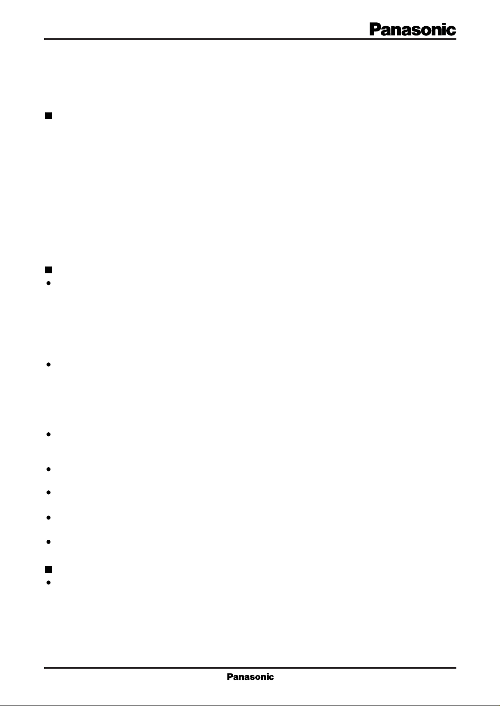
Pin Assignment
DD2DVSS2
VSDA
VSCK
V8CK
MOT
MTA1
MTA2
MTA3
MTA4
VPDA
VPCK
VPST
SH1
SH2
SH3
SH4
MTB1
MTB2
MTB3
MTB4
DV
U2TCK
U2SD
U2RCK
U2RD
U2ST
IRQ4
IRQ3
IRQ2
IRQ1
U1TCK
U1SD
VIR
VSEN
UC0
UC1
UC2
UC3
A23
A22
A21
A20
A19
A18
A17
A16
A15
DV
DV
A14
A13
A12
A11
A10
SS3
DD3
A9
A8
A7
A6
A5
A4
A3
A2
A1
A0
96959493929190898887868584838281807978777675747372717069686766
97
98
99
100
101
102
103
104
105
106
107
108
109
110
111
112
113
114
115
116
117
118
119
120
121
122
123
124
125
126
127
128
12345678910111213141516171819202122232425262728293031
65
64
63
62
61
60
59
58
57
56
55
54
53
52
51
50
49
48
47
46
45
44
43
42
41
40
39
38
37
36
35
34
33
U1RCK
U1RD
U1ST
S15
S14
S13
S12
S11
S10
S9
S8
S7
S6
S5
S4
S3
S2
S1
S0
MOD3
MOD2
MOD1
MOD0
VREFL
VREFH
AV
DD
IREF0
IREF1
TXLPIN
AV
SS
TXOUT
HV
DD
32
MD7
MD6
MD5
MD4
MD3
MD2
MD1
MD0
SYNCA
CX
SCX2
SS1
RD
DD1
WR
DV
DV
HDRES
QFH128-P-1818
BA
RNW
HALT
EQMD
EYCY
ADCK
SS4
PLSD
DV
DD4
DV
SHIN
AGCOUT
AGCIN
HPOUT
RXL
IREF2
RXLPIN
Page 3

For Communications Equipment MN195001
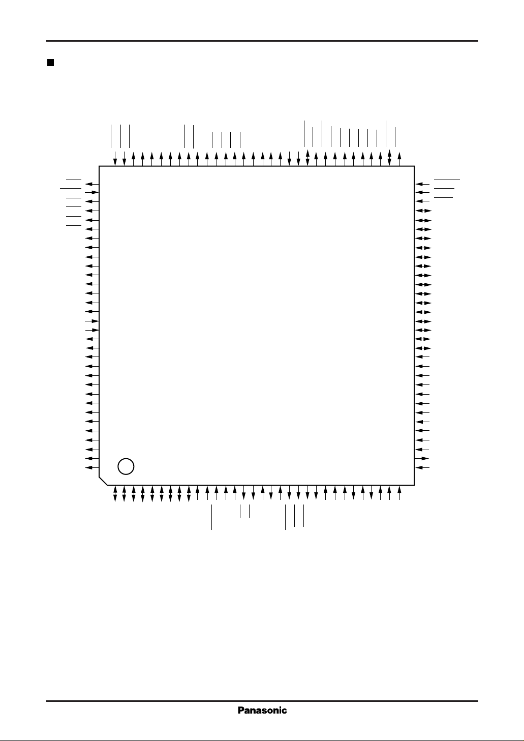
Block Diagram
VREFH
VREFL
IREF2 to 0
TXLPIN
TXOUT
RXLPIN
RXL
HPOUT
AGCIN
AGCOUT
SHIN
HV
DD
CX
SCX2
SYNCA
MOD3 to 0
HDRES
DV
DD4 to 1
DV
SS4 to 1
DD
AV
39
Analog front-end processor
(AFP)
11
10
9
42-45
Digital signal processor and CPU core
12
SS
AV
35
19
HALT
MTA4 to 1
MTB4 to 1
MOT
SH4 to 1
Clock
generator
DTE
I/F
VBCK
VIR
VSCK
VSEN
VSDA
VPCK
VPST
VPDA
Facsimile
peripheral
control
circuits
S15 to 0
UC3 to 0
IRO4 to 1
ADCK
EYSY
EOMD
PLSD
UITCK
U1SD
U1RCK
U1RD
Dual-port
RAM
U1ST
U2TCK
U2SD
U2RCK
U2RD
U2ST
18
BA
A23 to 0, MD7 to 0, RD, WR, R/W
Page 4

MN195001 For Communications Equipment
Pin Descriptions
Functional
Group
Symbol Pin No. I/O Function Descreption
A0 to 23
MD0 to 7 8 to 1 I/O External memory data bus
RD 16 O External memory read signal
WR 15 O External memory write signal
R/W 17 I External memory read/write control
Memory Interface
CX 11 I Basic clock input
SCX2 10 I Basic clock frequency selection
SYNCA 9 O System clock output
HDRES 12 I Reset signal
MOD0 to 3 42 to 45 I Mode setting inputs
HALT 19 I HALT signal for internal digital signal processor
Control Interface
BA 18 O External memory bus available signal
IREF0 38 AI D/A converter input
IREF1 37 AI Reference voltage for transmit circuits
TXLPIN 36 AI Transmit low-pass filter input
TXOUT 34 AO Analog transmit signal output
RXL 32 AI Analog receive signal input
IREF2 31 AI Reference voltage for receive circuit
RXLPIN 30 AI Receive low-pass filter input
HPOUT 29 AO Receive high-pass filter output
AGCIN 28 AI Receive automatic gain control input
Analog Interface
AGCOUT 27 AO Receive automatic gain control output
SHIN 26 AI A/D converter sample-and-hold circuit input
VREFH 40 AI A/D converter reference "H" level
VREFL 41 AI A/D converter reference "L" level
PLSD 23 O External amplifier gain control signal
SO to 15 46 to 61 I/O General-purpose I/O port
UC0 to 3 99 to 102 O Programmable chip select
IRO1 to 4 67 to 70 I External interrupts
U1ST 62 I USART (CH1) external synchronization clock
U1RD 63 I USART (CH1) receive data
U1RCK 64 I USART (CH1) receive clock
U1SD 65 O USART (CH1) transmit data
U1TCK 66 I/O USART (CH1) transmit clock
U2ST 71 I USART (CH2) external synchronization clock
Fax control Signals
U2RD 72 I USART (CH2) receive data
U2RCK 73 I USART (CH2) receive clock
U2SD 74 O USART (CH2) transmit data
U2TCK 75 I/O USART (CH2) transmit clock
SH1 to 4 85 to 82 O Thermal head control signals
MTA1 to 4 92 to 89 O Motor A control signals
128 to 114, 111 to 103
O External memory address bus
Page 5

For Communications Equipment MN195001
Pin Descriptions (continued)
Functional
Group
EYE
I/F
Symbol Pin No. I/O Function Description
MTB1 to 4 81 to 78 O Motor B control signals
MOT 93 O Motor synchronization signal
VPST 86 O Plotter data clock
VPCK 87 O Plotter synchronization burst clock
VPDA 88 O Plotter data
V8CK 94 O Scanner clock
VSCK 95 I Scanner data input clock
Fax Control Signals
VSDA 96 I Scanner data
VIR 97 O Scanner input ready
VSEN 98 I Scanner data input enable
ADCK 21 O Eye pattern data clock
EYSY 22 O Eye pattern data synchronization signal
EQMD 20 O Eye pattern data
DV
DD1 to 4
DV
SS1 to 4
AV
AV
Power Supply
Interface
HV
13, 77, 114, 25 DP Power supply for digital circuits +5 V
14, 76, 112, 24 DP Power supply for digital circuits GND
DD
SS
DD
39 AP Power supply for analog circuits +5 V
35 AP Power supply for analog circuits GND
33 AO HVDD output
Page 6

MN195001 For Communications Equipment
Package Dimensions (Unit: mm)
QFH128-P-1818
20.0±0.2
18.0
±0.2
96 65
97
(1.25)
64
(1.25)
18.0±0.2
20.0±0.2
33128
132
–0.05
+0.10
1.0±0.2
0.5
0.2±0.1
3.3±0.2
3.4±0.3
0.15
0.1
SEATING PLANE
0.1±0.1
0.5±0.2
0 to 10°
 Loading...