

Page 1
For Communications Equipment
MN195902
Digital Signal Processor for Image CODEC
Overview
The MN195902 is a high-speed, programmable digital
signal processor based on a vector pipeline architecture
for image processing applications. It incorporates many
features that make it ideal for highly efficient coding and
decoding of still and moving pictures in applications
involving the transmission, storage, and retrieval of
images.
Features
Flexible support for complex processing by simply
rewriting the contents of its internal program memory
Built-in dedicated hardware effective for image
CODEC, including
• Discrete cosine transform (DCT) converter
• Two-dimensional address generator
Architecture that links internal memory, a generalpurpose arithmetic unit, dedicated arithmetic unit, and
other components with a pipeline to better support
vector calculations, multiply-and-accumulate, and
other key image processing operations
ITU-T H.261 coding for the QCIF size (176 × 144)
with a decoding rate of 15 frames per second or higher
Applications
Image-based communications:
Moving picture videophones, video
conferencing systems, cable television
systems, image LANs, remote monitoring
systems, etc.
Image storage and retrieval:
Electronic still cameras, optical disc files,
image databases, etc.
Multimedia computers
Page 2
MN195902 For Communications Equipment
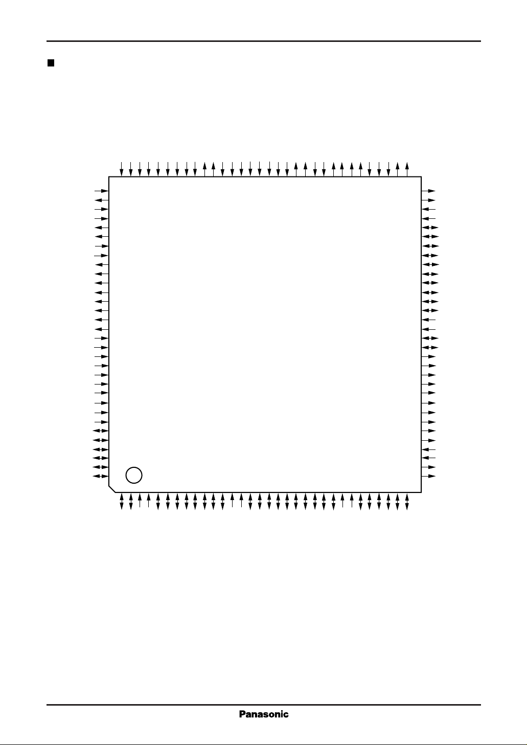
Pin Assignment
XSIEMP
SIRCLK
S1
XSOBSY
SOWCLK
S0
V
DD5
V
SS5
P0[7]
P0[6]
P0[5]
P0[4]
P0[3]
P0[2]
P0[1]
P0[0]
P0[7]
P0[6]
P0[5]
P0[4]
P0[3]
P0[2]
P0[1]
P0[0]
V
DD4
V
SS4
D2[15]
D2[14]
D2[13]
D2[12]
D2[11]
D2[10]
TEST1
DRMODE0
DRMODE1
SS6VDD6
V
XWCS
XSRE
ST1
ST2
XHLD/RUN
XRST
SPCLK
TEST0
96959493929190898887868584838281807978777675747372717069686766
97
XCS
XSWE
SS7
DD7
DRMODE2
V
SCLK
V
X801
X802
XRESEN1
XRESEN2
XOE1
XOE2
XWE1
XWE2
TEST2
98
99
100
101
102
103
104
105
106
107
108
109
110
111
112
113
114
115
116
117
118
119
120
121
122
123
124
125
126
127
128
12345678910111213141516171819202122232425262728293031
DDH
TEST3
V
XCAS1
XCAS2
65
64
63
62
61
60
59
58
57
56
55
54
53
52
51
50
49
48
47
46
45
44
43
42
41
40
39
38
37
36
35
34
33
32
XRAS1
XRAS2
V
SS8
V
DD8
A1[0]
A1[1]
A1[2]
A1[3]
A1[4]
A1[5]
A1[6]
A1[7]
A1[8]
A1[9]
V
SS9
V
DD9
A1[10]
A1[11]
A2[0]
A2[1]
A2[2]
A2[3]
A2[4]
A2[5]
A2[6]
A2[7]
A2[8]
A2[9]
V
SS10
V
DD10
A2[10]
A2[11]
D2[9]
D2[8]
V
DD3
SS3
V
D2[7]
D2[6]
D2[5]
D2[4]
D2[3]
D2[2]
SS2
DD2
V
V
D2[1]
D2[0]
D1[15]
LQFP128-P-1818
D1[14]
D1[13]
D1[12]
D1[11]
D1[9]
D1[10]
D1[8]
D1[7]
DD1
V
D1[6]
SS1
V
D1[5]
D1[4]
D1[3]
D1[2]
D1[1]
D1[0]
Page 3
For Communications Equipment MN195902
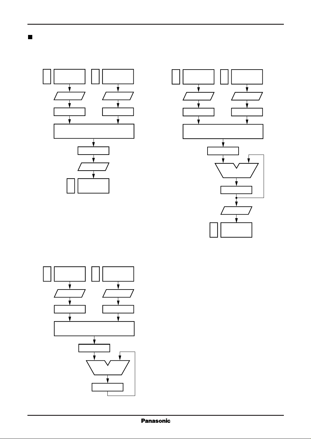
Vector Pipeline Processing Examples
SAG
P instruction
Internal
memory
SFT
REG
Pipeline arithmetic unit
REG
SFT
Internal
memory
SAG
SAG
Internal
memory
SFT
REG
SAG
QP instruction
Internal
memory
SFT
REG
Pipeline arithmetic unit
REG
SAG
SAG
ADD
REG
SFT
Internal
memory
Internal
memory
SFT
REG
SAG
Q instruction
Internal
memory
SFT
REG
Pipeline arithmetic unit
REG
SAG
Internal
memory
SFT
REG
ADD
REG
Page 4
MN195902 For Communications Equipment
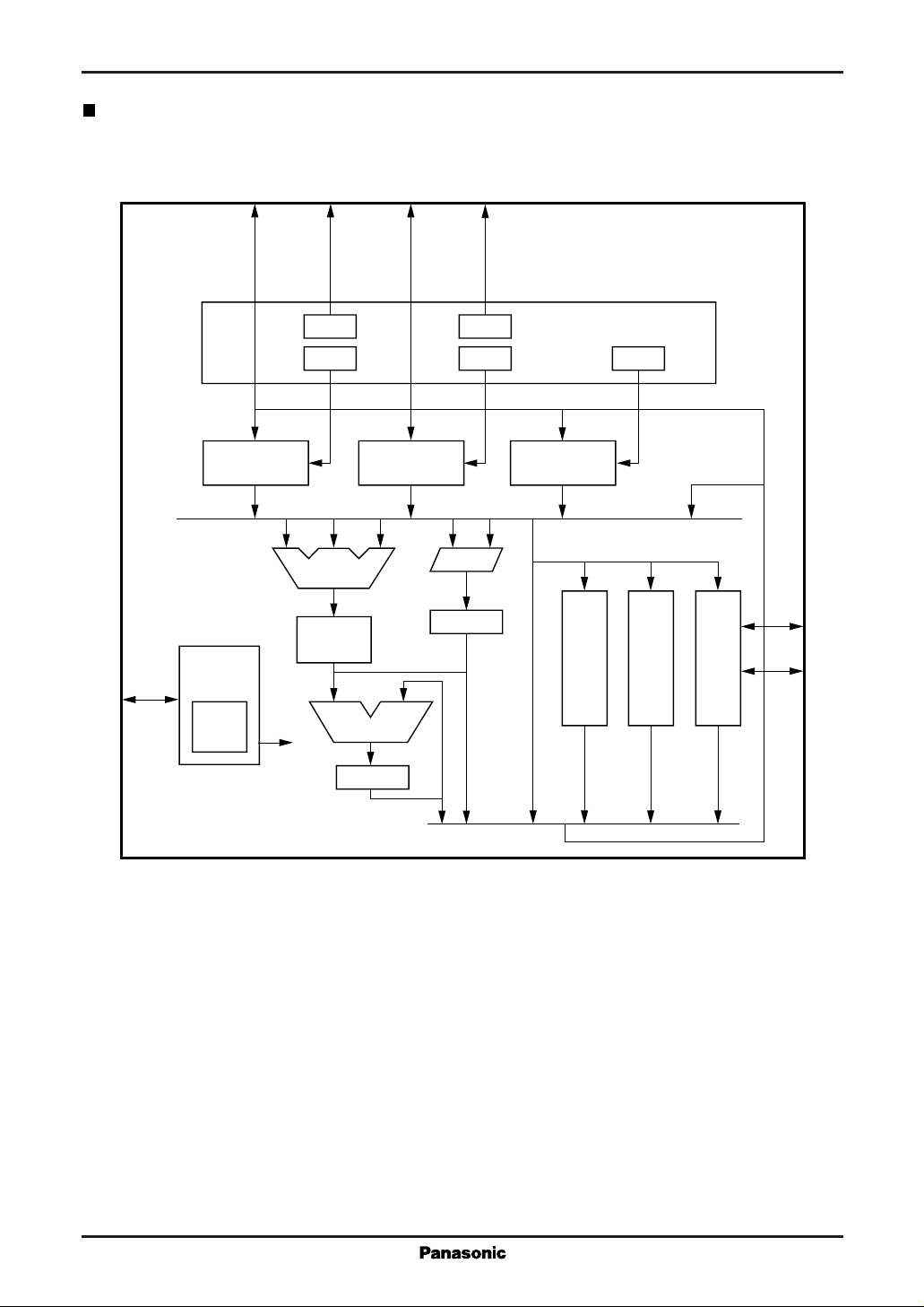
Block Diagram
CTL
Program
CTL
BM1
1Kwd
D1
A1
SAG SAG
SAG
EALU
FREG
16wd
D2
SAG
BM2
1Kwd
MPY
REG
A2
DM
1Kwd
DCT FLT
DRAM IF
SAG
SIO
PIO
SIO
PIO
IRAM
2Kwd
ACC
REG
SAG Two-dimensional address generator
BM1 Internal memory (1024 × 16 bits)
BM2 Instruction memory (2048 × 16 bits)
DM Instruction memory (2048 × 16 bits)
IRAM, IROM Instruction memory (2048 × 32 bits)
FREG0 to 15 General-purpose registers
EALU Arithmetic unit
MPY Multiplier
ACC Accumulator
DCT Discrete cosine transform converter
FLT Filter
SIO Serial interface
PIO Parallel interface
Page 5
For Communications Equipment MN195902
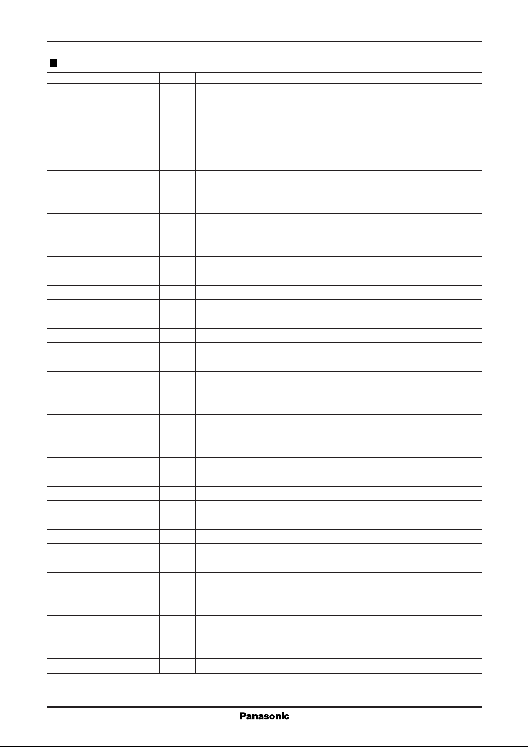
Pin Descriptions
Pin No. Symbol I/O Function Description
15 to 24, D1 (15:0) I/O/Z Data bus for data transfers to and from external memory (EM1)
27 to 32
47 to 48, A1 (11:0) I/O/Z Address bus for data transfers to and from external memory (EM1)
51 to 60
71 XWE1 O/Z External memory write control output (negative logic)
73 XOE1 O/Z External memory read control output (negative logic)
77 XBO1 O External memory cycle bus occupation control output (negative logic)
64 XRAS1 O/Z External memory row address strobe output (negative logic)
66 XCAS1 O/Z External memory row address strobe output (negative logic)
75 XRFSEN1 I External memory refresh enable signal (negative logic)
123 to 128, D2 (15:0) I/O/Z Data bus for data transfers to and from external memory (EM2)
1, 2, 5 to 12
33, 34, A2 (11:0) O/Z Address bus for data transfers to and from external memory (EM2)
37 to 46
70 XWE2 O/Z External memory write control output (negative logic)
72 XOE2 O/Z External memory read control output (negative logic)
76 XBO2 O External memory cycle bus occupation control output (negative logic)
63 XRAS2 O/Z External memory row address strobe output (negative logic)
65 XCAS2 O/Z External memory row address strobe output (negative logic)
74 XRFSEN2 I External memory refresh enable signal (negative logic)
79 SCLK I System clock input
96 SPCLK I Serial port clock input
85 XHLD/RUN I Operational mode transition control input
83 XCS I Chip select input (negative logic)
82 XSWE I Internal memory write enable input for Hold/Slave mode (negative input)
88 XSRE I Internal memory read enable input for Hold/Slave mode (negative input)
84 XRST I Reset input (negative input)
87 ST1 O Operating status output
86 ST2 O Operating status output
102 SO O/Z Serial out port data
101 SOWCLK O/Z Serial out port external write enable output
100 XSOBSY I Serial out port external busy input (negative logic)
99 SI I Serial in port data
98 SIRCLK O/Z Serial in port external read enable output
97 XSIEMP I Serial in port external external empty input (negative logic)
105 to 112 PO (7:0) O Parallel out port data bus (PO7 is MSB)
113 to 120 PI (7:0) I Parallel in port data bus (PI7 is MSB)
81, 92, 93 DRMODE(2:0) I External DRAM mode control inputs
V
dd
V
ddh
V
ss
I Power supply pin 3.3[V]
I Power supply pin 5.0 to Vdd[V]
I Power supply pin 0 [V]
Page 6
MN195902 For Communications Equipment
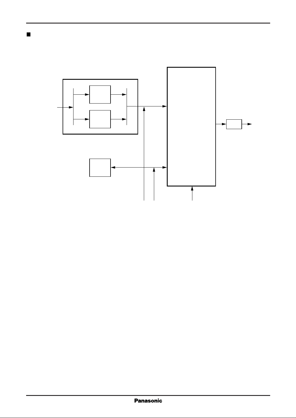
Application Circuit Example
Image input
Double buffer
(for input data)
Memory
(DRAM)
Memory
(DRAM)
(for local retrieval)
Memory
(DRAM)
Program load
MN195902
Port-1
Port-2
Execution control
Serial
port
FIFO
Code
Page 7
For Communications Equipment MN195902
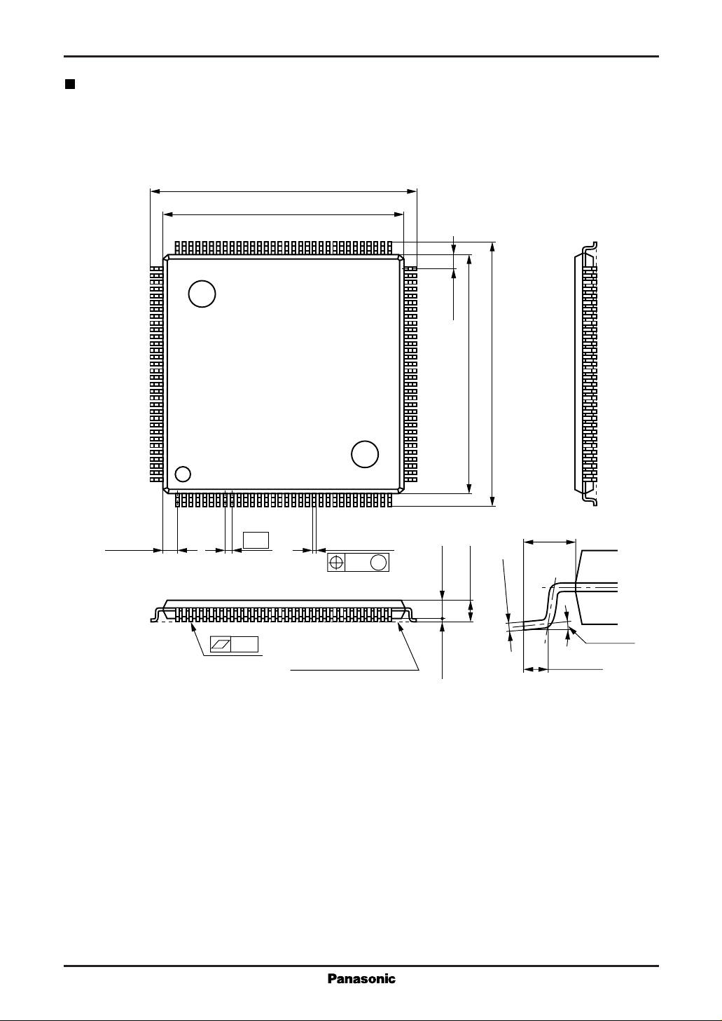
Package Dimensions (Unit: mm)
LQFP128-P-1818
20.0
±0.2
18.0
±0.1
96 65
97
128
(1.25)
64
(1.25)
±0.2
±0.1
20.0
18.0
33
132
0.5
0.2
0.1M
+0.10
–0.05
±0.1
1.4
1.7max.
(1.0)
±0.1
0.17
0 to 10°
0.1
SEATING PLANE
±0.1
0.1
0.5
±0.2
 Loading...