

Page 1
TL/F/5888
MM54C89/MM74C89 64-Bit TRI-STATE Random Access Read/Write Memory
March 1988
MM54C89/MM74C89 64-Bit TRI-STATE
É
Random Access Read/Write Memory
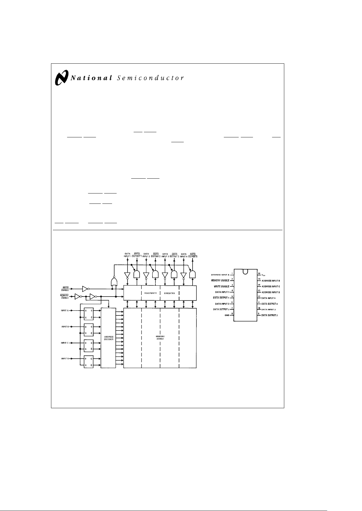
General Description
The MM54C89/MM74C89 is a 16-word by 4-bit random access read/write memory. Inputs to the memory consist of
four address lines, four data input lines, a write
enable line
and a memory
enable line. The four binary address inputs
are decoded internally to select each of the 16 possible
word locations. An internal address register latches the address information on the positive to negative transition of
the memory enable input. The four TRI-STATE data output
lines working in conjunction with the memory enable input
provide for easy memory expansion.
Address Operation: Address inputs must be stable t
SA
pri-
or to the positive to negative transition of memory
enable.It
is thus not necessary to hold address information stable for
more than t
HA
after the memory is enabled (positive to neg-
ative transition of memory
enable).
Note: The timing is different than the DM7489 in that a positive to negative
transition of the memory
enable must occur for the memory to be
selected.
Write Operation: Information present at the data inputs is
written into the memory at the selected address by bringing
write
enable and memory enable low.
Read Operation: The complement of the information which
was written into the memory is non-destructively read out at
the four outputs. This is accomplished by selecting the desired address and bringing memory
enable low and write
enable high.
When the device is writing or disabled the output assumes a
TRI-STATE (Hi-z) condition.
Features
Y
Wide supply voltage range 3.0V to 15V
Y
Guaranteed noise margin 1.0V
Y
High noise immunity 0.45 VCC(typ.)
Y
Low power fan out of 2
TTL compatibility driving 74L
Y
Low power consumption 100 nW/package (typ.)
Y
Fast access time 130 ns (typ.) at V
CC
e
10V
Y
TRI-STATE output
Logic and Connection Diagrams
TL/F/5888– 1
Dual-In-Line Package
TL/F/5888– 2
Top View
Order Number MM54C89
or MM74C89
TRI-STATEÉis a registered trademark of National Semiconductor Corporation.
C
1995 National Semiconductor Corporation RRD-B30M105/Printed in U. S. A.
Page 2
Absolute Maximum Ratings (Note 1)
If Military/Aerospace specified devices are required,
please contact the National Semiconductor Sales
Office/Distributors for availability and specifications.
Voltage at any Pin
b
0.3V to V
CC
a
0.3V
Operating Temperature Range
MM54C89
b
55§Ctoa125§C
MM74C89
b
40§Ctoa85§C
Storage Temperature Range (TS)
b
65§Ctoa150§C
Power Dissipation (P
D
)
Dual-In-Line 700 mW
Small Outline 500 mW
Operating V
CC
Range 3.0V to 15V
Absolute Maximum V
CC
18V
Lead Temperature (TL)
(Soldering, 10 seconds) 260
§
C
DC Electrical Characteristics Min/Max limits apply across temperature range, unless otherwise noted
Symbol Parameter Conditions Min Typ Max Units
CMOS TO CMOS
V
IN(1)
Logical ‘‘1’’ Input Voltage V
CC
e
5.0V 3.5 V
V
CC
e
10V 8.0 V
V
IN(0)
Logical ‘‘0’’ Input Voltage V
CC
e
5.0V 1.5 V
V
CC
e
10V 2.0 V
V
OUT(1)
Logical ‘‘1’’ Output Voltage V
CC
e
5.0V, I
O
eb
10 mA 4.5 V
V
CC
e
10V, I
O
eb
10 mA 9.0 V
V
OUT(0)
Logical ‘‘0’’ Output Voltage V
CC
e
5.0V, I
O
ea
10 mA 0.5 V
V
CC
e
10V, I
O
ea
10 mA 1.0 V
I
IN(1)
Logical ‘‘1’’ Input Current V
CC
e
15V, V
IN
e
15V
b
0.005 1.0 mA
I
IN(0)
Logical ‘‘0’’ Input Current V
CC
e
15V, V
IN
e
0V
b
1.0
b
0.005 mA
I
OZ
Output Current in High V
CC
e
15V, Ve15V 0.005 1.0 mA
Impedance State V
CC
e
15V, V
O
e
0V
b
1.0
b
0.005 mA
I
CC
Supply Current V
CC
e
15V 0.05 300 mA
CMOS/LPTTL INTERFACE
V
IN(1)
Logical ‘‘1’’ Input Voltage 54C, V
CC
e
4.5V V
CC
b
1.5 V
74C, V
CC
e
4.75V V
CC
b
1.5 V
V
IN(0)
Logical ‘‘0’’ Input Voltage 54C, V
CC
e
4.5V 0.8 V
74C, V
CC
e
4.75V 0.8 V
V
OUT(1)
Logical ‘‘1’’ Output Voltage 54C, V
CC
e
4.5V, I
O
eb
360 mA 2.4 V
74C, V
CC
e
4.75V, I
O
eb
360 mA 2.4 V
V
OUT(0)
Logical ‘‘0’’ Output Voltage 54C, V
CC
e
4.5V, I
O
ea
360 mA 0.4 V
74C, V
CC
e
4.75V, I
O
ea
360 mA 0.4 V
OUTPUT DRIVE (See 54C/74C Family Characteristics Data Sheet) (Short Circuit Current)
I
SOURCE
Output Source Current V
CC
e
5.0V, V
OUT
e
0V
b
1.75
b
3.3 mA
(P-Channel) T
A
e
25§C
I
SOURCE
Output Source Current V
CC
e
10V, V
OUT
e
0V
b
8.0
b
15 mA
(P-Channel) T
A
e
25§C
I
SINK
Output Sink Current V
CC
e
5.0V, V
OUT
e
V
CC
1.75 3.6 mA
(N-Channel) T
A
e
25§C
I
SINK
Output Sink Current V
CC
e
10V, V
OUT
e
V
CC
8.0 16 mA
(N-Channel) T
A
e
25§C
Note 1: ‘‘Absolute Maximum Ratings’’ are those values beyond which the safety of the device cannot be guaranteed. Except for ‘‘Operating Range’’ they are not
meant to imply that the devices should be operated at these limits. The table of ‘‘Electrical Characteristics’’ provides conditions for actual device operation.
AC Electrical Characteristics* T
A
e
25§C, C
L
e
50 pF, unless otherwise noted
Symbol Parameter Conditions Min Typ Max Units
t
pd
Propagation Delay from V
CC
e
5V 270 500 ns
Memory Enable V
CC
e
10V 100 220 ns
t
ACC
Access Time from V
CC
e
5V 350 650 ns
Address Input V
CC
e
10V 130 280 ns
t
SA
Address Setup Time V
CC
e
5V 150 ns
V
CC
e
10V 60 ns
t
HA
Address Hold Time V
CC
e
5V 60 ns
V
CC
e
10V 40 ns
t
ME
Memory Enable Pulse Width V
CC
e
5V 400 250 ns
V
CC
e
10V 150 90 ns
2
Page 3

AC Electrical Characteristics* T
A
e
25§C, C
L
e
50 pF, unless otherwise noted (Continued)
Symbol Parameter Conditions Min Typ Max Units
t
SR
Write Enable Setup V
CC
e
5V 0 ns
Time for a Read V
CC
e
10V 0 ns
t
WS
Write Enable Setup V
CC
e
5V t
ME
ns
Time for a Write V
CC
e
10V t
ME
ns
t
WE
Write Enable Pulse Width V
CC
e
5V, t
WS
e
0 300 160 ns
V
CC
e
10V, t
WS
e
0 100 60 ns
t
HD
Data Input Hold Time V
CC
e
5V 50 ns
V
CC
e
10V 25 ns
t
SD
Data Input Setup V
CC
e
5V 50 ns
V
CC
e
10V 25 ns
t1H,t
0H
Propagation Delay from a Logical V
CC
e
5V, C
L
e
5 pF, R
L
e
10k 180 300 ns
‘‘1’’ or Logical ‘‘0’’ to the High V
CC
e
10V, C
L
e
5 pF, R
L
e
10k
b
85 120 ns
Impedance State from
Memory Enable
t1H,t
0H
Propagation Delay from a Logical V
CC
e
50V, C
L
e
5 pF, R
L
e
10k 180 300 ns
‘‘1’’ or Logical ‘‘0’’ to the High V
CC
e
10V, C
L
e
5 pF, R
L
e
10k 85 120 ns
Impedance State from
Write Enable
C
IN
Input Capacity Any Input (Note 2) 5 pF
C
OUT
Output Capacity Any Output (Note 2) 6.5 pF
C
PD
Power Dissipation Capacity (Note 3) 230 pF
*AC Parameters are guaranteed by DC correlated testing.
Note 2: Capacitance is guaranteed by periodic testing.
Note 3: C
PD
determines the no load AC power consumption of any CMOS device. For complete explanation see 54C/74C Family Characteristics application note,
AN-90.
AC Electrical Characteristics* Guaranteed across the specified temperature range, C
L
e
50 pF
MM54C89 MM74C89
Parameter Conditions T
A
eb
55§Ctoa125§CT
A
eb
40§Ctoa85§C Units
Min Max Min Max
t
PD
V
CC
e
5V 700 600 ns
V
CC
e
10V 310 265 ns
V
CC
e
15V 250 210 ns
t
ACC
V
CC
e
5V 910 780 ns
V
CC
e
10V 400 345 ns
V
CC
e
15V 320 270 ns
t
SA
V
CC
e
5V 210 180 ns
V
CC
e
10V 90 80 ns
V
CC
e
15V 70 60 ns
t
HA
V
CC
e
5V 80 70 ns
V
CC
e
10V 55 50 ns
V
CC
e
15V 45 40 ns
t
ME
V
CC
e
5V 560 480 ns
V
CC
e
10V 210 180 ns
V
CC
e
15V 170 150 ns
t
WE
V
CC
e
5V 420 360 ns
V
CC
e
10V 140 120 ns
V
CC
e
15V 110 100 ns
t
HD
V
CC
e
5V 70 60 ns
V
CC
e
10V 35 30 ns
V
CC
e
15V 30 25 ns
*AC Parameters are guaranteed by DC correlated testing.
3
Page 4

AC Electrical Characteristics*
Guaranteed across the specified temperature range, C
L
e
50 pF (Continued)
MM54C89 MM74C89
Parameter Conditions T
A
eb
55§Ctoa125§CT
A
eb
40§Ctoa85§C Units
Min Max Min Max
t
SD
V
CC
e
5V 70 60 ns
V
CC
e
10V 35 30 ns
V
CC
e
15V 30 25 ns
t1H,t
0H
V
CC
e
5V 420 360 ns
V
CC
e
10V, C
L
e
5 pF 170 145 ns
V
CC
e
15V, R
L
e
10 kX 135 115 ns
*AC Parameters are guaranteed by DC correlated testing.
Truth Table
ME WE Operation Condition of Outputs
L L Write TRI-STATE
L H Read Complement of Selected Word
H L Inhibit, Storage TRI-STATE
H H Inhibit, Storage TRI-STATE
AC Test Circuits
t
0H
TL/F/5888– 4
t
1H
TL/F/5888– 3
Switching Time Waveforms
t
0H
TL/F/5888– 5
t
1H
TL/F/5888– 6
Read Cycle
TL/F/5888– 7
Write Cycle
TL/F/5888– 8
4
Page 5

Switching Time Waveforms (Continued)
Read Modify Write Cycle
TL/F/5888– 9
Note: t
r
e
60 ns
t
f
e
10 ns
5
Page 6

MM54C89/MM74C89 64-Bit TRI-STATE Random Access Read/Write Memory
Physical Dimensions inches (millimeters)
Ceramic Dual-In-Line Package (J)
Order Number MM54C89J or MM74C89J
NS Package Number J16A
Molded Dual-In-Line Package (N)
Order Number MM54C89N or MM74C89N
NS Package Number N16E
LIFE SUPPORT POLICY
NATIONAL’S PRODUCTS ARE NOT AUTHORIZED FOR USE AS CRITICAL COMPONENTS IN LIFE SUPPORT
DEVICES OR SYSTEMS WITHOUT THE EXPRESS WRITTEN APPROVAL OF THE PRESIDENT OF NATIONAL
SEMICONDUCTOR CORPORATION. As used herein:
1. Life support devices or systems are devices or 2. A critical component is any component of a life
systems which, (a) are intended for surgical implant support device or system whose failure to perform can
into the body, or (b) support or sustain life, and whose be reasonably expected to cause the failure of the life
failure to perform, when properly used in accordance support device or system, or to affect its safety or
with instructions for use provided in the labeling, can effectiveness.
be reasonably expected to result in a significant injury
to the user.
National Semiconductor National Semiconductor National Semiconductor National Semiconductor
Corporation Europe Hong Kong Ltd. Japan Ltd.
1111 West Bardin Road Fax: (
a
49) 0-180-530 85 86 13th Floor, Straight Block, Tel: 81-043-299-2309
Arlington, TX 76017 Email: cnjwge@tevm2.nsc.com Ocean Centre, 5 Canton Rd. Fax: 81-043-299-2408
Tel: 1(800) 272-9959 Deutsch Tel: (
a
49) 0-180-530 85 85 Tsimshatsui, Kowloon
Fax: 1(800) 737-7018 English Tel: (
a
49) 0-180-532 78 32 Hong Kong
Fran3ais Tel: (
a
49) 0-180-532 93 58 Tel: (852) 2737-1600
Italiano Tel: (
a
49) 0-180-534 16 80 Fax: (852) 2736-9960
National does not assume any responsibility for use of any circuitry described, no circuit patent licenses are implied and National reserves the right at any time without notice to change said circuitry and specifications.
 Loading...