

Page 1
TL/F/6137
MM5452/MM5453 Liquid Crystal Display Drivers
February 1995
MM5452/MM5453 Liquid Crystal Display Drivers
General Description
The MM5452 is a monolithic integrated circuit utilizing
CMOS metal gate, low threshold enhancement mode devices. It is available in a 40-pin molded package. The chip can
drive up to 32 segments of LCD and can be paralleled to
increase this number. The chip is capable of driving a 4 (/2digit 7-segment display with minimal interface between the
display and the data source.
The MM5452 stores display data in latches after it is
clocked in, and holds the data until new display data is received.
Features
Y
Serial data input
Y
No load signal required
Y
DATA ENABLE (MM5452)
Y
Wide power supply operation
Y
TTL compatibility
Y
32 or 33 outputs
Y
Alphanumeric and bar graph capability
Y
Cascaded operation capability
Applications
Y
COPSTMor microprocessor displays
Y
Industrial control indicator
Y
Digital clock, thermometer, counter, voltmeter
Y
Instrumentation readouts
Y
Remote displays
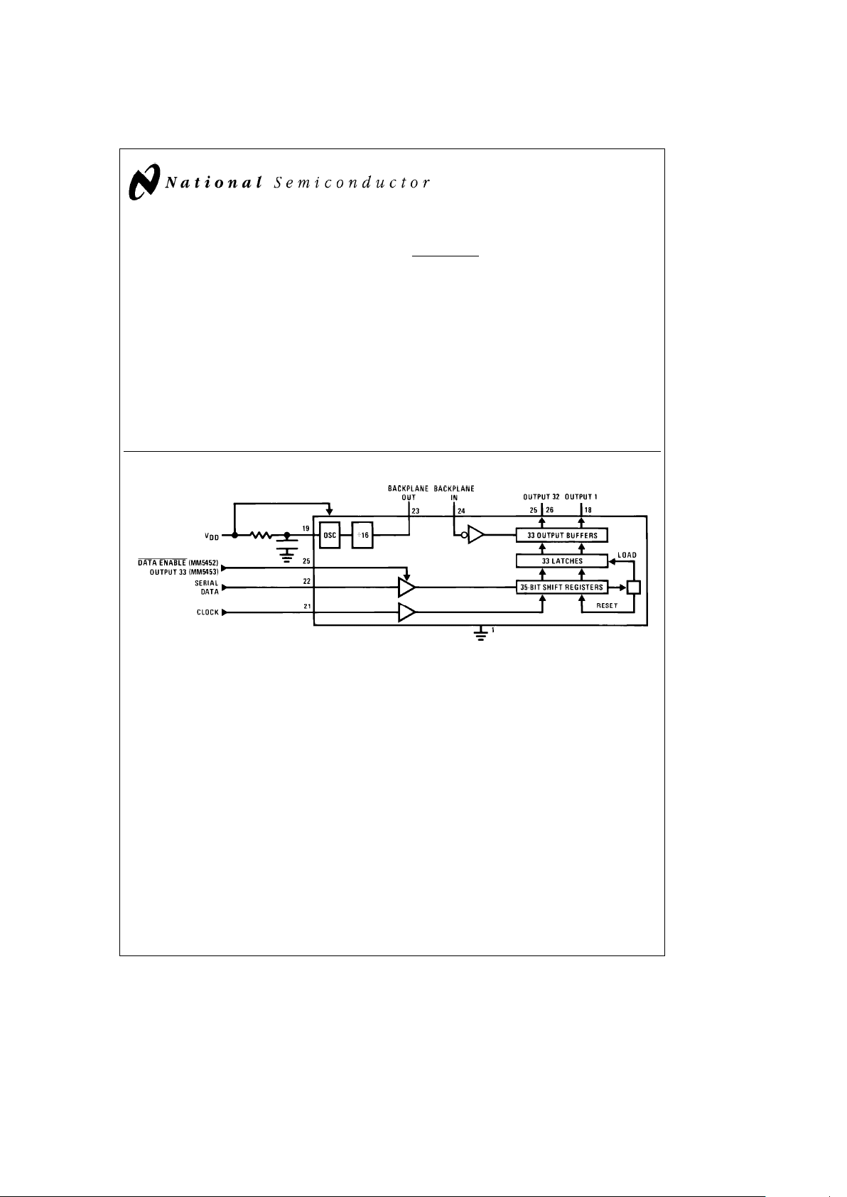
Block Diagram
TL/F/6137– 1
FIGURE 1
COPSTMis a trademark of National Semiconductor Corp.
C
1995 National Semiconductor Corporation RRD-B30M105/Printed in U. S. A.
Page 2
Absolute Maximum Ratings
If Military/Aerospace specified devices are required,
please contact the National Semiconductor Sales
Office/Distributors for availability and specifications.
Voltage at Any Pin V
SS
to V
SS
a
10V
Operating Temperature 0§Ctoa70§C
Storage Temperature
b
65§Ctoa150§C
Power Dissipation 300 mW ata70§C
350 mW at
a
25§C
Junction Temperature
a
150§C
Lead Temperature (Soldering, 10 sec.) 300§C
Electrical Characteristics
TAwithin operating range, V
DD
e
3.0V to 10V, V
SS
e
0V, unless otherwise specified
Parameter Conditions Min Typ Max Units
Power Supply 3 10 V
Power Supply Current Excluding Outputs
OSC
e
VSS,BPIN@32 Hz 40 mA
V
DD
e
5V, Open Outputs, No Clock 10 mA
Clock Frequency 500 kHz
Input Voltages
Logical ‘0’ Level V
DD
k
4.75
b
0.3 0.1 V
DD
V
V
DD
t
4.75
b
0.3 0.8 V
Logical ‘1’ Level V
DD
l
5.25 0.8 V
DD
V
DD
V
V
DD
s
5.25 2.0 V
DD
V
Output Current Levels
Segments
Sink V
DD
e
3V, V
OUT
e
0.3V
b
20 mA
Source V
DD
e
3V, V
OUT
e
V
DD
b
0.3V 20 mA
Backplane
Sink V
DD
e
3V, V
OUT
e
0.3V
b
320 mA
Source V
DD
e
3V, V
OUT
e
V
DD
b
0.3V 320 mA
Output Offset Voltage Segment Load 250 pF
g
50 mV
Backplane Load 8750 pF (Note 1)
Clock Input Frequency, f
C
(Notes 2 and 3) 500 kHz
High Time, t
h
950 ns
Low Time, t
l
950 ns
Data Input
Set-Up Time, t
DS
300 ns
Hold Time, t
DH
300 ns
Data Enable Input
100 ns
Set-Up Time, t
DES
Note 1: This parameter is guaranteed (not 100% production tested) over operating temperature and supply voltage ranges. Not to be used in Q.A. testing.
Note 2: AC input waveform for test purpose: t
r
s
20 ns, t
f
s
20 ns, fe500 kHz, 50%g10% duty cycle.
Note 3: Clock input rise and fall times must not exceed 300 ns.
2
Page 3
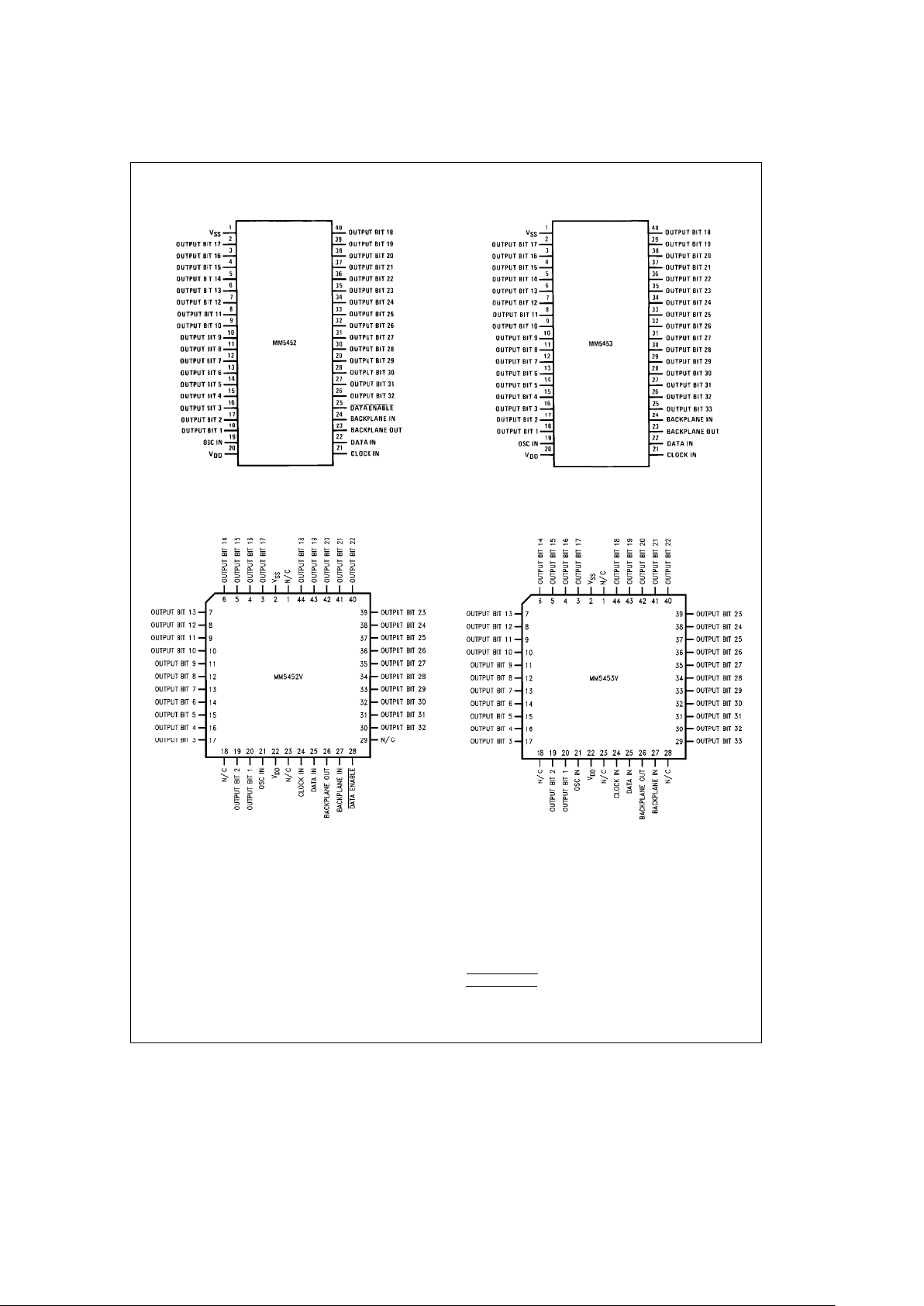
Connection Diagrams
Dual-In-Line Package
TL/F/6137– 2
Top View
FIGURE 2a
Plastic Chip Carrier
TL/F/6137– 11
Top View
Dual-In-Line Package
TL/F/6137– 3
Top View
FIGURE 2b
Plastic Chip Carrier
TL/F/6137– 12
Top View
Order Number MM5452N, MM5453N,
MM5452V or MM5453V
See NS Package Number N40A or V44A
Functional Description
The MM5452 is specifically designed to operate 4 (/2-digit 7segment displays with minimal interface with the display and
the data source. Serial data transfer from the data source to
the display driver is accomplished with 2 signals, serial data
and clock. Since the MM5452 does not contain a character
generator, the formatting of the segment information must
be done prior to inputting the data to the MM5452. Using a
format of a leading ‘‘1’’ followed by the 32 data bits allows
data transfer without an additional load signal. The 32 data
bits are latched after the 36th clock is complete, thus providing non-multiplexed, direct drive to the display. Outputs
change only if the serial data bits differ from the previous
time.
A block diagram is shown in
Figure 1.
For the MM5452 a
DATA ENABLE
is used instead of the 33rd output. If the
DATA ENABLE
signal is not required, the 33rd output can
be brought out. This is the MM5453 device.
3
Page 4

Functional Description (Continued)
Figure 4
shows the input data format. A start bit of logical
‘‘1’’ precedes the 32 bits of data. At the 36th clock a LOAD
signal is generated synchronously with the high state of the
clock, which loads the 32 bits of the shift registers into the
latches. At the low state of the clock a RESET signal is
generated which clears all the shift registers for the next set
of data. The shift registers are static master-slave configuration. There is no clear for the master portion of the first shift
register, thus allowing continuous operation.
If the clock is not continuous, there must be a complete set
of 36 clocks otherwise the shift registers will not clear.
Figure 2a
shows the pin-out of the MM5452. Bit 1 is the first
bit following the start bit and it will appear on pin 18.
Figure 3
shows the timing relationships between data, clock
and DATA ENABLE
.
TL/F/6137– 4
FIGURE 3
TL/F/6137– 5
FIGURE 4. Input Data Format
4
Page 5

Functional Description (Continued)
Figure 5
shows a typical application. Note how the input
data maps to the output pins and the display. The MM5452
and MM5453 do not have format restrictions, as all outputs
are controllable. This application assumes a specific display
pinout. Different display/driver connection patterns will, of
course, yield a different input data format.
TL/F/6137– 6
Consult LCD manufacturer’s data sheet for specific pinouts.
FIGURE 5. Typical 4(/2-Digit Display Application
5
Page 6

Functional Description (Continued)
TL/F/6137– 7
*The minimum recommended value for R for the oscillator input is 9 kX. An RC time constant of approximately
4.91
c
10
b
4
should produce a backplane frequency between 30 Hz and 150 Hz.
FIGURE 6. Parallel Backplane Outputs
TL/F/6137– 8
FIGURE 7. External Backplane Clock
Figure 8
shows a four wire remote display that takes advantage of the device’s serial input to move many bits of display
information on a few wires.
USING AN EXTERNAL CLOCK
The MM5452/MM5453 LCD Drivers can be used with an
externally supplied clock, provided it has a duty cycle of
50%. Deviations from a 50% duty cycle result in an offset
voltage on the LCD. In
Figure 7,
a flip-flop is used to assure
a 50% duty cycle. The oscillator input is grounded to prevent oscillation and reduce current consumptions in the
chips. The oscillator is not used.
Using an external clock allows synchronizing the display
drive with AC power, internal clocks, or DVM integration
time to reduce interference from the display.
Figure 9
is a general block diagram that shows how the
device’s serial input can be used to advantage in an analog
display. The analog voltage input is compared with a staircase voltage generated by a counter and a digital-to-analog
converter or resistor array. The result of this comparison is
clocked into the MM5452, MM5453. The next clock pulse
increments the staircase and clocks the new data in.
With a buffer amplifier, the same staircase waveform can be
used for many displays. The digital-to-analog converter
need not be linear; logarithmic or other non-linear functions
can be displayed by using weighted resistors or special
DACs. This system can be used for status indicators, spectrum analyzers, audio level and power meters, tuning indicators, and other applications.
6
Page 7

Functional Description (Continued)
TL/F/6137– 9
FIGURE 8. Four Wire Remote Display
TL/F/6137– 10
Data is high until staircaselinput
FIGURE 9. Analog Display
Physical Dimensions inches (millimeters)
Molded Dual-In-Line Package (N)
Order Number MM5452N or MM5453N
NS Package Number N40A
7
Page 8

MM5452/MM5453 Liquid Crystal Display Drivers
Physical Dimensions inches (millimeters) (Continued)
Plastic Chip Carrier (V)
Order Number MM5452V or MM5453V
NS Package Number V44A
LIFE SUPPORT POLICY
NATIONAL’S PRODUCTS ARE NOT AUTHORIZED FOR USE AS CRITICAL COMPONENTS IN LIFE SUPPORT
DEVICES OR SYSTEMS WITHOUT THE EXPRESS WRITTEN APPROVAL OF THE PRESIDENT OF NATIONAL
SEMICONDUCTOR CORPORATION. As used herein:
1. Life support devices or systems are devices or 2. A critical component is any component of a life
systems which, (a) are intended for surgical implant support device or system whose failure to perform can
into the body, or (b) support or sustain life, and whose be reasonably expected to cause the failure of the life
failure to perform, when properly used in accordance support device or system, or to affect its safety or
with instructions for use provided in the labeling, can effectiveness.
be reasonably expected to result in a significant injury
to the user.
National Semiconductor National Semiconductor National Semiconductor National Semiconductor
Corporation Europe Hong Kong Ltd. Japan Ltd.
1111 West Bardin Road Fax: (
a
49) 0-180-530 85 86 13th Floor, Straight Block, Tel: 81-043-299-2309
Arlington, TX 76017 Email: cnjwge@tevm2.nsc.com Ocean Centre, 5 Canton Rd. Fax: 81-043-299-2408
Tel: 1(800) 272-9959 Deutsch Tel: (
a
49) 0-180-530 85 85 Tsimshatsui, Kowloon
Fax: 1(800) 737-7018 English Tel: (
a
49) 0-180-532 78 32 Hong Kong
Fran3ais Tel: (
a
49) 0-180-532 93 58 Tel: (852) 2737-1600
Italiano Tel: (
a
49) 0-180-534 16 80 Fax: (852) 2736-9960
National does not assume any responsibility for use of any circuitry described, no circuit patent licenses are implied and National reserves the right at any time without notice to change said circuitry and specifications.
 Loading...