

Page 1
MM5369 17 Stage Oscillator/Divider
MM5369 17 Stage Oscillator/Divider
February 1995
General Description
The MM5369 is a CMOS integrated circuit with 17 binary
divider stages that can be used to generate a precise reference from commonly available high frequency quartz crystals. An internal pulse is generated by mask programming
the combinations of stages 1 through 4, 16 and 17 to set or
reset the individual stages. The MM5369 is advanced one
count on the positive transition of each clock pulse. Two
buffered outputs are available: the cyrstal frequency for tuning purposes and the 17th stage output. The MM5369 is
available in an 8-lead dual-in-line epoxy package.
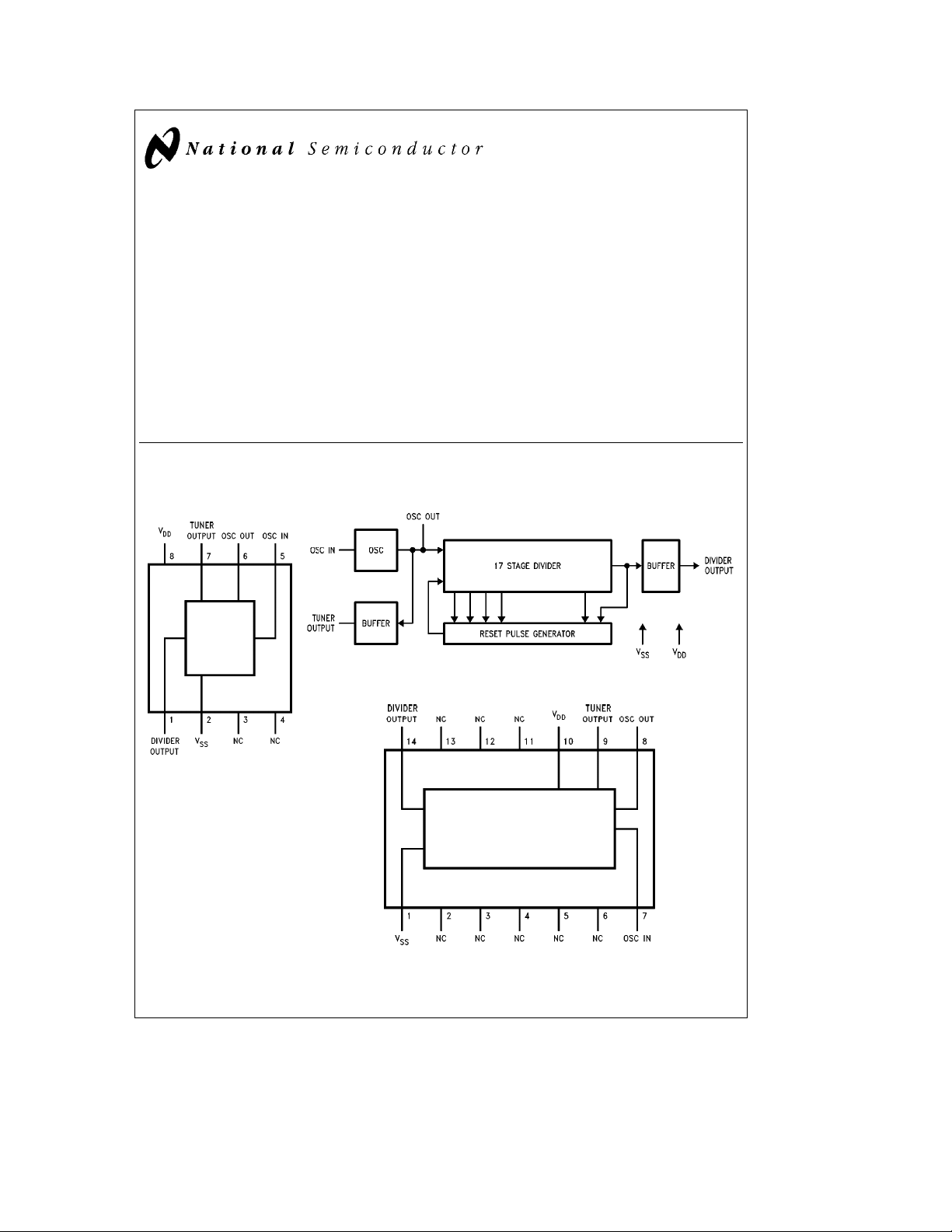
Connection and Block Diagrams
Dual-In-Line Package
Features
Y
Crystal oscillator
Y
Two buffered outputs
Output 1 crystal frequency
Output 2 full division
Y
High speed (4 MHz at V
Y
Wide supply range 3V –15V
Y
Low power
Y
Fully static operation
Y
8-lead dual-in-line package
Y
Low Current
DD
e
10V)
Option
Y
MM5369AA 3.58 MHz to 60 Hz
FIGURE 2
TL/F/10820– 2
Top View
TL/F/10820– 1
Order Number MM5369AA/N
See NS Package Number
N08E
Order Number MM5369AA/M
See NS Package Number M14A
C
1996 National Semiconductor Corporation RRD-B30M66/Printed in U. S. A.
TL/F/10820
TL/F/10820– 8
Page 2
Absolute Maximum Ratings
If Military/Aerospace specified devices are required,
please contact the National Semiconductor Sales
Office/Distributors for availability and specifications.
Voltage at Any Pin
Operating Temperature 0§Ctoa70§C
Storage Temperature
b
0.3V to V
b
65§Ctoa150§C
DD
a
0.3V
Package Dissipation 500 mW
Maximum V
Voltage 16V
CC
Operating VCCRange 3V to 15V
Lead Temperature (Soldering, 10 seconds) 300§C
Electrical Characteristics
TAwithin operating temperature range, V
e
SS
GND, 3VsV
Parameter Conditions Min Typ Max Units
Quiescent Current Drain V
Operating Current Drain V
Frequency of Oscillation V
Output Current Levels V
Logical ‘‘1’’ Source 500 mA
e
15V 10 mA
DD
e
DD
e
DD
e
V
DD
e
DD
e
V
O
e
10V, f
4.19 MHz 1.2 2.5 mA
IN
10V DC 4.5 MHz
6V DC 2 MHz
10V
5V
Logical ‘‘0’’ Sink 500 mA
Output Voltage Levels V
Logical ‘‘1’’ 9.0 V
e
10V
DD
e
I
10 mA
O
Logical ‘‘0’’ 1.0 V
Note: For 3.58 MHz operation, VDDmust bet10V.
s
15V unless otherwise specified.
DD
Functional Description
A connection diagram for the MM5369 is shown in
and a block diagram is shown in
Figure 2.
TIME BASE
A precision time base is provided by the interconnection of
a 3,579,545 Hz quartz crystal and the RC network shown in
Figure 3
together with the CMOS inverter/amplifier provided
between the OSC IN and the OSC OUT terminals. Resistor
R1 is necessary to bias the inverter for class A amplifier
operation. Capacitors C1 and C2 in series provide the parallel load capacitance required for precise tuning of the quartz
crystal.
The network shown provides
used with standard crystals trimmed for C
to better than
g
2 ppm is easily obtainable.
l
100 ppm tuning range when
L
Figure 1
e
12 pF. Tuning
DIVIDER
A pulse is genertaed when divider stages 1 through 4, 16
and 17 are in the correct state. By mask options, this pulse
is used to set or reset individual stages of the counter.
ure 4
shows the relationship between the duty cycle and the
programmed modulus.
OUTPUTS
The Tuner Output is a buffered output at the crystal oscillator frequency. This output is provided so that the crystal
frequency can be obtained without disturbing the crystal oscillator. The Divide Output is the input frequency divided by
the mask programmed number. Both outputs are push-pull
outputs.
Fig-
http://www.national.com 2
Page 3

Functional Description (Continued)
*To be selected based on xtal used
FIGURE 3. Crystal Oscillator Network
FIGURE 5. Typical Current Drain
vs Oscillator Frequency
TL/F/10820– 3
TL/F/10820– 4
FIGURE 4. Plot of Divide-By vs Duty Cycle
TL/F/10820– 6
FIGURE 6. Output Waveform for the MM5369AA
TL/F/10820– 5
http://www.national.com3
Page 4

http://www.national.com 4
Page 5

Physical Dimensions inches (millimeters) unless otherwise noted
14-Lead (0.150×Wide) Molded Small Outline Package (M)
Order Number MM5369AA/M
NS Package Number M14A
http://www.national.com5
Page 6

Physical Dimensions inches (millimeters) unless otherwise noted (Continued)
MM5369 17 Stage Oscillator/Divider
8-Lead Molded Dual-In-Line Package (N)
Order Number MM5369N
NS Package Number N08E
LIFE SUPPORT POLICY
NATIONAL’S PRODUCTS ARE NOT AUTHORIZED FOR USE AS CRITICAL COMPONENTS IN LIFE SUPPORT
DEVICES OR SYSTEMS WITHOUT THE EXPRESS WRITTEN APPROVAL OF THE PRESIDENT OF NATIONAL
SEMICONDUCTOR CORPORATION. As used herein:
1. Life support devices or systems are devices or 2. A critical component is any component of a life
systems which, (a) are intended for surgical implant support device or system whose failure to perform can
into the body, or (b) support or sustain life, and whose be reasonably expected to cause the failure of the life
failure to perform, when properly used in accordance support device or system, or to affect its safety or
with instructions for use provided in the labeling, can effectiveness.
be reasonably expected to result in a significant injury
to the user.
National Semiconductor National Semiconductor National Semiconductor National Semiconductor
Corporation Europe Hong Kong Ltd. Japan Ltd.
1111 West Bardin Road Fax:
Arlington, TX 76017 Email: europe.support@nsc.com Ocean Centre, 5 Canton Rd. Fax: 81-043-299-2408
Tel: 1(800) 272-9959 Deutsch Tel:
Fax: 1(800) 737-7018 English Tel:
http://www.national.com
National does not assume any responsibility for use of any circuitry described, no circuit patent licenses are implied and National reserves the right at any time without notice to change said circuitry and specifications.
Fran3ais Tel:
Italiano Tel:a49 (0) 180-534 16 80 Fax: (852) 2736-9960
a
49 (0) 180-530 85 86 13th Floor, Straight Block, Tel: 81-043-299-2308
a
49 (0) 180-530 85 85 Tsimshatsui, Kowloon
a
49 (0) 180-532 78 32 Hong Kong
a
49 (0) 180-532 93 58 Tel: (852) 2737-1600
 Loading...