

Page 1
MITSUMI
Step-Up DC/DC Converter (PWM) MM1349
Step-Up DC/DC Converter (PWM)
Monolithic IC MM1349
Outline
This is a converter IC which steps up the DC input voltage to output a fixed voltage level. Utilizing technology
for low-voltage operation, which is a feature of Mitsumi semiconductor processes, operation is possible
beginning at 0.90V, making this device ideal for the power supply circuits of portable equipment driven by a
single battery.
Because PWM oscillation is adopted, an output waveform can be obtained with a smaller peak-to-peak
voltage than is possible for VFM devices.
Features
1. Low-voltage operation possible, 0.90V (no-load)
2. Internal oscillation circuit
3. Adoption of PWM oscillation for output waveform with small peak-to-peak voltage
4. Numerous output voltages available (seven ranks)
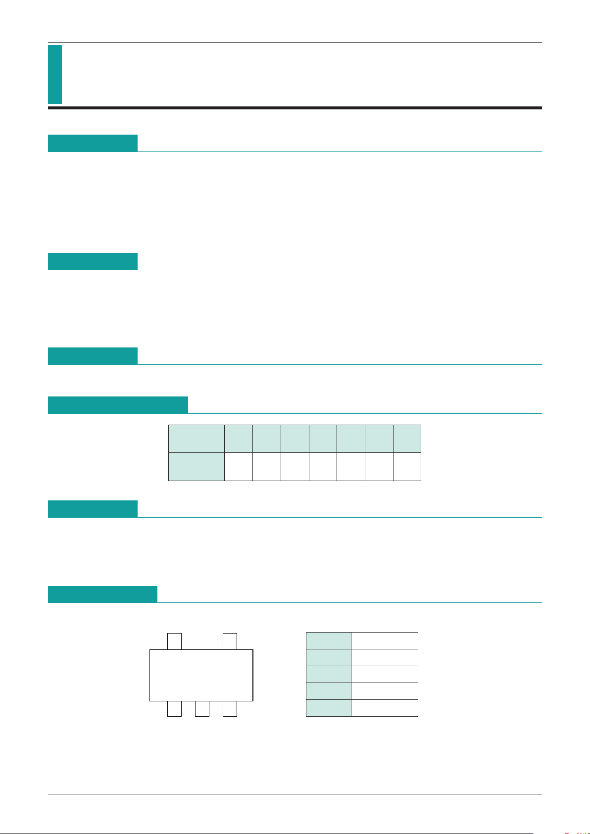
Package
SOT-25
Pin Assignment
13
5
2
4
SOT-25
Applications
1. Pagers
2. Separate vibrators
3. Other portable equipment
Output Voltage Rank
Rank A B C D E G H
Voltage (V) 5.0 3.5 3.2 3.0 2.7 2.5 2.2
1 GND
2 SUB
3 V
L
4 VOUT
5 VIN
*
Pin 2 is the SUB pin, and should be connected to GND.
Page 2

MITSUMI
Step-Up DC/DC Converter (PWM) MM1349
Block Diagram
Note: Pin 2 is the SUB pin, and should be connected to GND.
Absolute Maximum Ratings
(Ta=25°C)
Item Symbol Ratings Units
Storage temperature T
STG
-
40~+125 °C
Operating temperature T
OPR
-
20~+75 °C
Voltage applied to V
IN pin
-
0.3~+10.0 V
Voltage applied to V
OUT pin
-
0.3~+10.0 V
Voltage applied to V
L pin
-
0.3~+10.0 V
Allowable loss Pd 150 mW
Recommended Operating Conditions
Item Symbol Ratings Units
Operating temperature Top
-
20~+75 °C
Operating voltage Vop +0.9~V
OUT V
Page 3

MITSUMI
Step-Up DC/DC Converter (PWM) MM1349
Electrical Characteristics
(Ta=25°C)(Except where noted otherwise,VIN=1.5V, IO=1mA)
Item Symbol Measurement conditions Min. Typ. Max. Units
Operating voltage V
IN No-load 0.90 VOUT V
A 4.80 5.00 5.20
B 3.36 3.50 3.64
C 3.07 3.20 3.33
Output voltage V
OUT VIN=1.5V, Io=1mA D 2.88 3.00 3.12 V
E 2.59 2.70 2.81
F 2.40 2.50 2.60
G 2.11 2.20 2.29
Output voltage temperature coefficient
Ta=-20~75°C ±100
ppm/°C
Input fluctuations VIN=1.1 1.7V, Io=1mA 1 %/V
Load fluctuation V
IN=1.5V, Io=0 4mA 1
%/mA
Efficiency VIN=1.5V, Io=1mA 80 µA
V
L pin leakage current IVLLK VL=10V 1 µA
Oscillation frequency f
OSC VIN=1.5V, Io=1mA 35 65 95 kHz
Note: These characteristics assume the following externally mounted components.
Coil: L=120µH (Mitsumi model C5-R)
Capacitor: C=33µF (tantalum electrolytic capacitor)
Schottky barrier diode (Rohm model RB451F)
Measuring Circuit
Note 1: A: DC ammeter
V: DC voltmeter
Note 2: L=120µH
Application Circuits
Coil: L=120µH (Mitsumi model C5-R)
Capacitor: C=33µF (tantalum electrolytic capacitor)
Schottky barrier diode (Rohm model RB451F)
 Loading...