

Page 1
MITSUMI
Control for Lithium Ion Battery Charging (one cell) MM1333
Control for Lithium Ion Battery Charging (one cell)
Monolithic IC MM1333
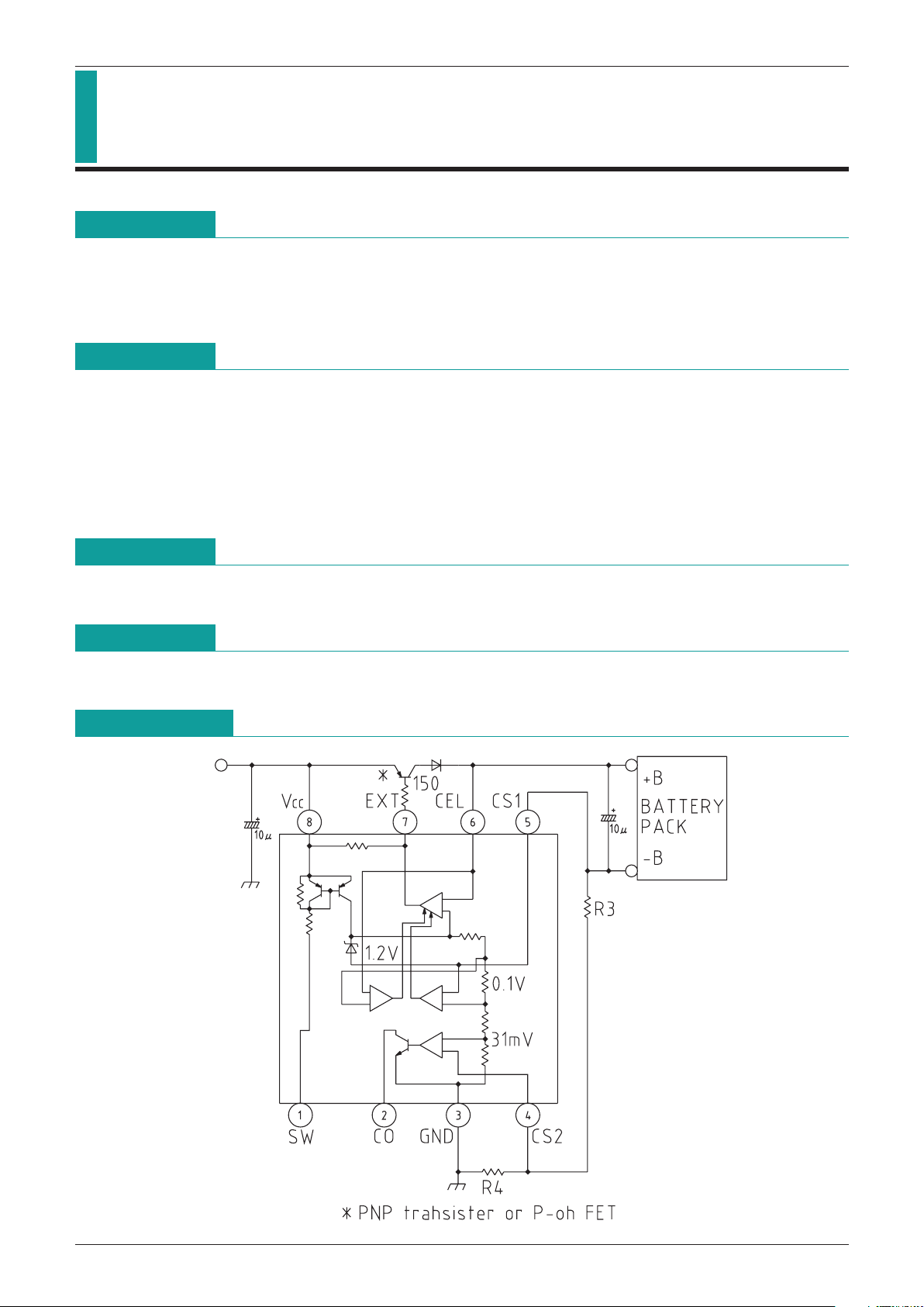
Outline
This IC was developed for use in charging lithium ion batteries. A power transistor or P-MOS FET is mounted
externally to control charging. This IC is for use with a single cell only, and provides precise control of the
charging voltage ; the charging current can be set through an external resistance. In addition to the functions
of the MM1332, it incorporates a comparator for full-charge detection.
Features
1. Output voltage (Ta=25°C) 4.100V±35mV
2. Output voltage (Ta=
-
20°C~+70°C) 4.100V±50mV
3. Constant-current output Current limit 100mV±10mV
Constant current value = current limit/external resistance
4. Low-voltage (LV) detection function 2.00V±100mV
5. Full-charge detection function Detection voltage 31mV±5mV
Package
SOP-8C
Applications
1. Lithium ion battery chargers
MITSUMI
Block Diagram
Page 2
MITSUMI
Control for Lithium Ion Battery Charging (one cell) MM1333
Pin Assignment
Pin Description
Values given are standard
1432
8567
SOP-8C
1 SW
2 CO
3 GND
4 CS2
5 CS1
6 CEL
7 EXT
8 V
CC
Pin no. Pin name
Input/output
Function
1 SW Input
Input pin for on/off control
SW=V
CC : off, SW=GND : on
Pulled up to V
CC, so turned off when open
Full-charge signal output pin
While charging : Open collector output NPN transistor is off
At full charge : Open collector output NPN transistor is on
2 CO output
GROUND pin
3 GND Input
Full charge detection pin
The current is detected through the voltage drop across an external
resistance, to control the full-charge signal.
The ratio of the charge current set by CS1 and the current at full-charge signal
output is (VIC)/(0.1 V R4/(R3+R4))
4 CS2 Input
Current detection pin
The current is detected through the voltage drop across an external
resistance, to maintain a constant current. The current value can be set using
0.1 V/(R3+R4).
5 CS1 Input
6 CEL Input
Battery voltage input pin
The battery voltage is detected and used to maintain the voltage at the
prescribed value.
A low-voltage detection circuit is also present, and charging is forbidden when
the battery voltage is less than 2V.
Constant-voltage circuit output pin
The base of an external PNP transistor or gate of a P-ch FET is controlled in
constant-voltage charging.
7 EXT Output
8 V
CC Input
Power supply input pin
Absolute Maximun Ratings
(Ta=25°C)
Item Symbol Ratings Units
Storage temperature T
STG
-
40~+125 °C
Operating temperature T
OPR
-
20~+70 °C
Power supply voltage V
CC max.
-
0.3~+13 V
Output voltage V
O max.
-
0.3~VCC V
SW input voltage V
SW
-
0.3~VCC+0.3 V
Allowable loss Pd 300 mW
Page 3

MITSUMI
Control for Lithium Ion Battery Charging (one cell) MM1333
Recommended Operating Conditions
Electrical Characteristics
(Except where noted otherwise, Ta=25°C, VCC=5V, SW2, 4, 6, 7 : A)
MITSUMI
Item Symbol Ratings Units
Operating temperature T
OPR
-
20~+70 °C
Operating voltage V
OPR +5~+12 V
Item Symbol Measurement conditions Min. Typ. Max. Units
Consumption current 1 I
CC1 VSW=0V (Charge : ON) 300 400 µA
Consumption current 2 I
CC2 VSW=0V (Charge : ON) 1.1 1.6 mA
Consumption current 3 I
CC3 VSW=VCC (Charge : OFF) 2 4 µA
Output voltage 1 V
O1 Ta=25°C 4.065 4.100 4.135 V
Output voltage 2 V
O2 Ta=0~+40°C 4.050 4.100 4.150 V
Output voltage temperature drift V
O Ta=
-
20~+70°C ±0.25
mV
°C
Current limit V
CL 90 100 110 mV
CEL-CS leakage current I
CEL 1µA
SW input current I
SW 20 µA
SW input voltage
V
L Charge : ON
-
0.3 2.0 V
V
H Charge : OFF
VCC-
1.0 VCC+0.3
V
Low-voltage detection voltage L
V 1.90 2.00 2.10 V
EXT pin input voltage I
S 10 20 mA
EXT pin output voltage V
EXT No load 0.3
VCC-
0.3
V
Full-charge detection voltage V
IC 26 31 36 mV
Full-charge detection output L V
COL ISINK=0.3mA 0.2 0.4 V
Full-charge detection
output leakage current
I
CO 1µA
Page 4

MITSUMI
Control for Lithium Ion Battery Charging (one cell) MM1333
Measurement Method
(Except where noted otherwise, Ta=25°C, VCC=5V, SW2 : A, SW4 : A, SW6 : A, SW7 :
MITSUMI
Item Measurement Method
Consumption
current 1
Set V1=0 V, SW4=B, V4=50mV, V6=4.5V ; switch SW6 from A to B and again to A ; then measure the
A8 current I
CC1.
Consumption
current 2
Set V1=0V, SW4=B, V4=50mV, V6=4.5V ; switch SW6 from A to B and again to A ; then measure the
A8 current I
CC1.
Consumption
current 3
Set V1=VCC, and measure the resulting A8 current ICC3.
Output voltage
Set V1=0V, V6=4.5V; switch SW6 from A to B and again to A ; then measure the T6 voltage VO.
Current limit
Set V1=0V, set the voltage V6 about 1V lower than the potential at T6 (output voltage), and set SW6
to B ; then measure the T5 voltage V
CL.
CEL-CS
leakage current
Set VCC=0V, V1=0V; set the voltage V6 to 5V; and set SW6 to B and SW7 to C. Then measure the A6
current I
CEL.
SW input current
With V1=0V, measure the A1 current ISW1.
SW input voltage
Set the voltage V6 1V lower than the T6 potential (output voltage), and set SW6 to B. With the
voltage V1 variable, when the A6 current is 100mA or higher this voltage is equal to the charge-on
voltage (VL), and when the current is within ±10µA it is equal to the charge-off voltage (VH).
Low-voltage
detection voltage
Set V1=0 V, set V6 to 1V lower than the T6 potential (output voltage), and set switch SW6 to B. Then
gradually lower the voltage V6 ; the voltage V6 at which the A6 current is within ±10µA is LV.
EXT pin input
voltage
Measure the A7 current IS with V1=0V, SW6 set to B, SW7 set to B, V6=3V, and V7=4V.
EXT pin output
voltage
Set V1=0 V, SW6 to B, and SW7 to C. The T7 voltage when V6=3V and V6=5V is VEXT.
Full-charge
detection voltage
Set V1=0V and SW4 to B. Gradually lower the voltage V4 from 50mV ; the voltage V4 when the T2
potential falls to 1V or lower from (V
CC-1) V or higher is VIC.
Full-charge
detection output L
Measure the T2 voltage VCOL when V1=0V, SW4 is at B and V4=0V.
Full-charge
detection output
leakage current
Measure the A2 current ICO when V1=0V, SW4 is at B, V4=50mV, SW2 is at B, and V2=5V.
Warnings regarding use
1. The following components should be added in preparation for use.
1. A capacitance of several µF or so between V
CC and GND
2. A 10µF capacitor between CEL and CS
3. A diode to prevent backflow between the collector of the external PNP transistor and pin 6
4. A current-limiting 150Ω resistor between the base of the external PNP transistor and EXT
2. The full charge detection circuit detects voltages of order several mV, and so no hysteresis is applied.
Chattering will occur, and should be born in mind.
3. There is an internal low-voltage detection circuit. If a voltage of at least 2V is not applied to the CEL pin, no
output will be obtained.
Page 5

MITSUMI
Control for Lithium Ion Battery Charging (one cell) MM1333
Timing Chart
VCC
OFF
OFF ON
ON
SW
CEL
CS1,2
(When R3=0)
Battery connected and SW on
CS1,2
(When R3=0)
CO
CO
CEL
Charge off
Charge off
Charge on signal
With CO pulled up to V
CC by a resistance
Full-charge signal
Charge on
Normal charging
Low battery voltage
(2V or lower)
0
0
0
100mV
0
0
0
0
0
H
H
L
L
31mV
2
2
Page 6

MITSUMI
Control for Lithium Ion Battery Charging (one cell) MM1333
Application circuits
1. A diode prevents backflow from the battery.
2. By inserting R2 for adjustment, even higher precision can be achieved.
3. The charging current can be set using R3+R4.
4. The full charge detection voltage can be adjusted through the ratio of R3 to R4. (The detection voltage can
be raised)
5. R5 and R6 are resistances used for positive feedback (hysteresis). Hysteresis is in proportion to the voltage
drop across R5. Here the full charge detection voltage also changes in proportion to the voltage drop
across R5. (The detection voltage falls)
The above diagram is an example for reference; in actual applications, the circuit constants and circuit
operation should first be thoroughly studied.
Page 7

MITSUMI
Control for Lithium Ion Battery Charging (one cell) MM1333
Charging (VCC=5V, Output voltage 4.1V)
Maximum output voltage vs power supply voltage
Maximum output voltage vs power supply voltage
Input bias current vs temperature
Output voltage vs ambient temperature
(V
CC=5V, Output voltage 4.1V)
Output voltage vs power supply voltage
(Ta=25°C, Output voltage 4.1V)
4.15
4.14
4.13
4.12
4.11
4.1
4.09
4.08
4.07
4.06
4.05
Output voltage (V)
-
25 0 25 50 75
Ambient temperature (°C)
4.15
4.14
4.13
4.12
4.11
4.1
4.09
4.08
4.07
4.06
4.05
56789101112131415161718
Power supply voltage (V)
Output voltage (V)
4.5
4.4
4.3
4.2
4.1
4
3.9
3.8
3.7
3.6
3.5
Power supply voltage V (V)
0 0.5 1 1.5 2 2.5 3
Charging time (h)
12
8
4
0
-
4
-
8
-
12
24681012
Power supply voltage V+/V
-
(±V)
Maximum output voltage VO (V)
Characteristics
30
25
20
15
10
5
0
0.1 1 10
Load resistance RL (Ω)
Maximum output voltage
amplitude V
OPP (V)
60
50
40
30
20
Input bias current IB (nA)
-
25 25 50 85
Ambient temperature Ta (°C)
Maximum output voltage amplitude vs frequency
Voltage gain frequency characteristic
25
20
15
10
5
0
10 100 1000 10000 1000001000000
Frequency f (Hz)
Maximum output voltage
amplitude V
OPP (V)
1 10 100 1000
10000
100000
1000000 10000000
Frequency f (Hz)
Voltage gain AV (dB)
120
100
80
60
40
20
0
MITSUMI
Page 8

MITSUMI
Control for Lithium Ion Battery Charging (one cell) MM1333
MITSUMI
Input offset voltage vs power supply voltage
Input offset voltage temperature
Current consumption temperature Input offset current temperature
Input-equivalent noise voltage frequency Input-equivalent noise voltage vs signal
source resistance
1 10 100 1000
Frequency f (Hz)
1000
100
10
1
Input-equivalent noise
voltage en (nV/ Hz)
10 100 1000 10000
Signal source resistance Rs (Ω)
10
1
0.1
Input-equivalent noise
voltage en (µVrms)
246881012
Power supply voltage V+/V
-
(±V)
0.5
0.4
0.3
0.2
0.1
0
-
0.1
-
0.2
-
0.3
-
0.4
-
0.5
Input offset voltage VIO (mV)
0.5
0.4
0.3
0.2
0.1
0
-
0.1
-
0.2
-
0.3
-
0.4
-
0.5
-
25 25 50 85
Ambient temperature Ta (°C)
Input offset voltage VIO (mV)
-
25 25 50 85
Ambient temperature Ta (°C)
5
4.5
4
3.5
3
2.5
2
Current consumption ICC (mA)
-
25 25 50 85
Ambient temperature Ta (°C)
5
4
3
2
-
1
1
0
-
2
-
3
-
4
-
5
Input offset current IIO (nA)
Output current (S
INK
) vs power supply voltage Output current (SOURCE) vs power supply
2 4 6 8 10 12
Power supply voltage V+/V
-
(±V)
Output current ISINK (mA)
20
15
10
5
2 4 6 8 10 12
Power supply voltage V+/V- (±V)
Output current ISOURCE
ISOURCE (mA)
-
5
-
10
-
15
-
20
Page 9

MITSUMI
Control for Lithium Ion Battery Charging (one cell) MM1333
Input offset current vs power supply voltage
Input bias current vs power supply voltage
Output current (SINK) temperature Output current (SOURCE) temperature
-
25 25 50 85
Ambient temperature Ta (°C)
20
15
10
5
Output current ISINK (mA)
-
25 25 50 85
Ambient temperature Ta (°C)
-
5
-
10
-
15
-
20
Output current ISOURCE (mA)
2 4 6 8 10 12
Power supply voltage V+/V
-
(±V)
5
4
3
2
-
1
1
0
-
2
-
3
-
4
-
5
Input offset current IIO (nA)
2 4 6 8 10 12
Power supply voltage V+/V
-
(±V)
50
40
20
30
10
0
Input bias current IB (nA)
35
30
25
-
25 25 75 85
Ambient temperature (°C)
H-rank full charge detection voltage (mV)
25
20
15
-
25 25 75 85
Ambient temperature (°C)
D-rank full charge detection voltage (mV)
H-rank full charge detection voltage [mV] D-rank full charge detection voltage [mV]
Page 10

MITSUMI
Control for Lithium Ion Battery Charging (one cell) MM1333
0 5 10 15 20
4.15
4.10
4.05
Power supply voltage (V)
H-rank output voltage (V)
0 5 10 15 20
4.25
4.20
4.18
4.15
Power supply voltage (V)
D-rank output voltage(V)
-
25 25 75 85
2.1
2.0
1.9
Ambient temperature (°C)
Low-voltage detection voltage (V)
-
25 25 75 85
110
100
90
Ambient temperature (°C)
CS1 pin voltage (mV)
25
-
25 75 85
4.15
4.10
4.05
Ambient temperature (°C)
H-rank output voltage(V)
-
25 25 75 85
4.25
4.20
4.15
Ambient temperature (°C)
D-rank output voltage(V)
H-rank output voltage [V] D-rank output voltage [V]
Low-voltage detection voltage [V] CS1 pin voltage [V]
H-rank output voltage [V] D-rank output voltage [V]
 Loading...