

Page 1

MITSUMI
Low-Saturation Three-Pin Regulators with Externally Mounted Power Transistor MM1215 and 1216
Low-Saturation Three-Pin Regulators with Externally Mounted Power Transistor
Monolithic ICs MM1215 and 1216
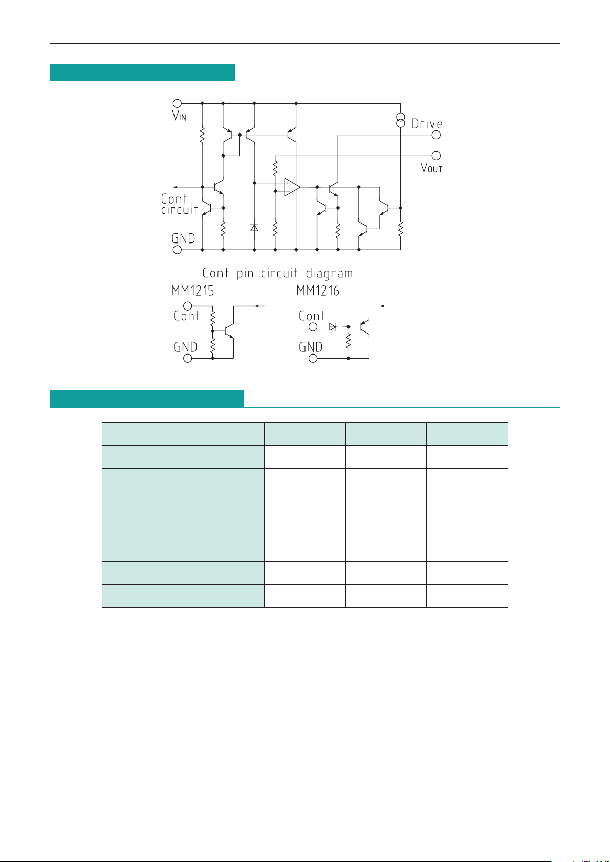
Outline
These ICs are high-precision, high-voltage stabilized power supply devices which, by employing an externally
mounted power transistor are able to drive loads at large currents. The input/output voltage difference is a low
0.2V, and an internal protection circuit ensures that the devices can be used in a wide range of portable
equipment. Output on/off control is also provided.
Features
1. Input voltage 16V max.
2. Input/output voltage difference 0.2V typ.
3. Maximum driving current 15mA max.
4. No-load input current 250µA typ.
5. Thermal shutdown circuit provided
6. Output ranks E : 9.0V±2% I : 4.0±2%
F : 6.0V±2% J : 3.0±2%
G : 5.0V±2% Z : 3.3±2%
H : 4.5V±2%
Package
SOT-25A (MM1215 N, MM1216 N)
*
The output voltage rank appears in the boxes.
Applications
1. Handheld computers
2. Portable transceivers
3. Cordless phones
4. Other portable equipment which uses batteries
Model Low High
MM1215 ON OFF
MM1216 OFF ON
CONT Pin Output Logic
1 Drive
2 GND
3 CONT
4 V
IN
5 VOUT
54
123
SOT-25A
Pin Assignment
Page 2
MITSUMI
Low-Saturation Three-Pin Regulators with Externally Mounted Power Transistor MM1215 and 1216
Equivalent Circuit Diagram
Absolute Maximum Ratings
Item Symbol Ratings Units
Storage temperature T
STG
-
40~+125 °C
Operating temperature T
OPR
-
20~+75 °C
Power supply voltage Vd max.
-
0.3~16 V
Recommended power supply voltage
VIN 2.5~12 V
CONT pin voltage V
COH1
-
0.3~VIN+0.3 V
Recommended driving current 0~10 mA
Allowable loss Pd 150 mW
Page 3

MITSUMI
Low-Saturation Three-Pin Regulators with Externally Mounted Power Transistor MM1215 and 1216
Electrical Characteristics
(Ta=25°C) : Using the 2SB956 output transistor
Item Symbol Measurement conditions Min. Typ. Max. Unit
E 9.00
F 6.00
G 5.00
Output voltage Vo VIN=Vo+1V Io=100mA H
Vo-2%
4.50
Vo+2%
V
I 4.00
J 3.00
Z 3.30
Consumption current Iccql V
IN=Vo+1V 250 400 µA
Minimum I/O voltage difference Vd min. V
IN=Vo
-
0.1V 0.2 0.3 V
Input fluctuation rate V2 V
IN=(Vo+1V)~12V
±0.01 ±0.1
%/V
Load fluctuation rate V1 V
IN=Vo+1V, Io=0~500mA
±0.01 ±0.03
%/mA
Output voltage temperature coefficient
Vo/T Tj=-20~+75°C ±100
ppm/°C
Ripple rejection rate RR
V
IN=Vo+2V, f=120Hz
50 60 dB
V
RIPPLE=1V, Io=100mA
Output noise voltage VN
V
IN=Vo+1V, Io=100mA
150
µVrms
f=10~80kHz
MM1215
Input current while off Iccq2 V
IN=Vo+1V 25 40 µA
C
ONT pin current ION VCONT=0.6V 1 3 µA
C
ONT pin current IOFF VCONT=2.4V 5 10 µA
MM1216
Input current while off Iccq2 V
IN=Vo+1V 25 40 µA
C
ONT pin current ION VCONT=2.4V 5 10 µA
C
ONT pin current IOFF VCONT=0.6V 1 3 µA
CONT pin level
High V
h 2.4 V
Low V
L 0.6 V
Page 4

MITSUMI
Low-Saturation Three-Pin Regulators with Externally Mounted Power Transistor MM1215 and 1216
Measuring Circuit
Measurement circuit 1 Measurement circuit 2
Note: When the C
ONT pin is unused, it should be connected to ground for the MM1215 and to Vcc for the
MM1216.
Characteristics
(MM1215)
3
4
5
2
1
0
0123456
Input voltage (V)
Output voltage (V)
0
0 100 200 300 400 500
0.1
0.2
0.3
0.4
0.5
Output current (mA)
I/O voltage difference (V)
300
400
500
200
100
0
0 2 4 6 8 1012141618
Input voltage (V)
Consuption current (µA)
-
5
00
4 6 8 101214 1816
5
10
15
20
-
10
-
15
-
20
Output voltage (V)
Input fluctuation rate (mV)
Output voltage characteristic No-load input current
I/O voltage difference (V
IN=2.8V) Input fluctuation rate
Page 5

MITSUMI
Low-Saturation Three-Pin Regulators with Externally Mounted Power Transistor MM1215 and 1216
0
0 100 200 300 400 500
10
20
30
-
10
-
20
-
30
Output current (mA)
Load fluctuation rate
Temperature (°C)
2.98
3
-
25 0 25 50 75 100 125
3.02
3.04
3.06
2.96
2.94
2.92
Output voltage (V)
Frequency (Hz)
10
20
30
40
50
60
70
80
90
100
0
10 100 1k 10k 100k
Ripple rejection rate (dB)
Load fluctuation
Output temperature characteristic
Ripple rejection rate
 Loading...