

MITSUMI
2-Input 2-Output Video Switch MM1120
2-Input 2-Output Video Switch
Monolithic IC MM1120
Outline
This is a 2-input, 2-output 3-circuit high performance video switch IC for video/audio signal switching. It is
ideal for use in TV/BS switching.
Features
1. 1 video signal circuit, 2 audio signal circuits
2. 1 built-in 75Ω driver circuit
3. Current consumption 17mA typ.
4. Operating power supply voltage range 9~12V
5. Frequency response 10MHz (V
OUT1), 7MHz (VOUT2)
6. Crosstalk Video signal circuit : 60dB (at 4.43MHz)
Audio signal circuit : 80dB (at 1kHz)
Package
SSOP-16A (MM1120XF)
Applications
1. TV with built-in BS
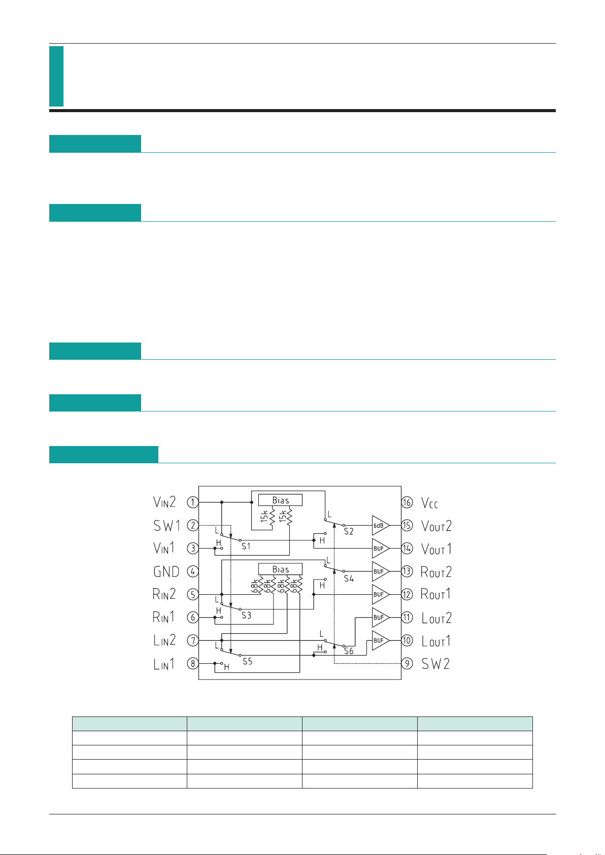
Block Diagram
Control input truth table
SW1 SW2 OUT1 OUT1
L L IN2 IN2
L H IN2 IN2
H L IN1 IN2
H H IN1 IN1
MITSUMI
2-Input 2-Output Video Switch MM1120
Pin Description
Pin no. Pin name Function Internal equivalent circuit diagram
1
V
IN Video input
3
2
SW Switch
9
14 VOUT1 Video output 1
10
R
OUT
11
and Audio output
12
L
OUT
13
5
R
IN
6
and Audio input
7
L
IN
8
4 GND Ground

MITSUMI
2-Input 2-Output Video Switch MM1120
15 VOUT2 Video output 2
16 V
CC Power supply
Absolute Maximum Ratings
(Ta=25°C)
Item Symbol Ratings Units
Storage temperature T
STG
-
40~+125 °C
Operating temperature T
OPR
-
20~+75 °C
Power supply voltage V
CC max. 15 V
Allowable loss Pd 500 mW
Electrical Characteristics
(Except where noted otherwise, Ta=25°C, VCC=8V~13V, V1=0V, V2=0V,
SG-1, SG-2, SG-3, no signal)
Item Symbol
Measurement
Measurement conditions Min. Typ. Max. Units
pin
Operating power supply voltage
VCC VCC 8.00 13.0 V
Consumption current
I
CC1VCC=9V 16.0 21.0 mA
I
CC2VCC=12V 17.0 22.0 mA
V
IN1
-
VOUT1 V1=V2=VCC, SW1 : B, VIN2-VOUT1, SW1 : A
Voltage gain G
V1 SG1 : Sine wave 1VP-P, 0.1MHz
-
0.5 0 0.5 dB
Frequency characteristic F
C1
TP2 SG1 : Sweep signal 1.0V
P-P
-
1.0 0 1.0 dB
10MHz/0.1MHz
Differential gain D
G1
SG1: Staircase wave 1V
P-P
0±3%
TP8
APL=10, 50, 90%
Differential phase D
P1
SG1: Staircase wave 1V
P-P
0 ±3 deg
APL=10, 50, 90%
V
IN2
-
VOUT2 SW1 : A, VIN1-VOUT2 V1=V2=VCC, SW1 : B
Voltage gain G
V2 SG1 : Sine wave 1VP-P, 0.1MHz 5.5 6.0 6.5 dB
Frequency characteristic F
C2
TP1 SG1 : Sweep signal 1.0V
P-P,
-
1.0 0 1.0 dB
7MHz/0.1MHz
Differential gain D
G2
SG1 : Staircase wave 1V
P-P
0±3%
TP7
APL=10, 50, 90%
Differential phase D
P2
SG1 : Staircase wave 1V
P-P
0 ±3 deg
APL=10, 50, 90%
R
IN1
-
ROUT1 V1=V2=VCC, SW2 : B, RIN2-ROUT1 SW2 : A
Voltage gain G
V3 SG2 : Sine wave 2.5VP-P, 1kHz
-
0.5 0 0.5 dB
Total harmonic distortion T
HD1 TP4 SG2 : Sine wave 2.5VP-P, 1kHz 0.01 0.1 %
Output noise voltage V
N1 15kHz band 3 50
µVrms
RIN2-ROUT2 SW2 : A, RIN1-ROUT2 V1=V2=VCC, SW2 : B
Voltage gain G
V4 SG2 : Sine wave 2.5VP-P, 1kHz
-
0.5 0 0.5 dB
Total harmonic distortion T
HD2 TP3
SSG2 : Sine wave 2.5V
P-P
, 1kHz
0.01 0.1 %
Output noise voltage V
N2 15kHz band 3 50
µVrms

MITSUMI
2-Input 2-Output Video Switch MM1120
LIN1-LOUT1 V1=V2=VCC, SW3 : B, LIN2-LOUT1 SW3 : A
Voltage gain G
V5 SG3 : Sine wave 2.5VP-P, 1kHz
-
0.5 0 0.5 dB
Total harmonic distortion T
HD3 TP6 SG3 : Sine wave 2.5VP-P, 1kHz 0.01 0.1 %
Output noise voltage V
N3 15kHz band 3 50
µVrms
LIN2-LOUT2 SW3 : A, LIN1-LOUT2 V1=V2=VCC, SW3 : B
Voltage gain G
V6 SG3 : Sine wave 2.5VP-P, 1kHz
-
0.5 0 0.5 dB
Total harmonic distortion T
HD4 TP5 SG3 : Sine wave 2.5VP-P, 1kHz 0.01 0.1 %
Output noise voltage V
N4 15kHz band 3 50
µVrms
Output offset voltage
V
OUT1 Voff1 TP2
DC level difference when V1=0V and V1=Vcc
0 ±15 mV
V
OUT2 Voff2 TP1
DC level difference when V2=0V and V2=Vcc
0 ±30 mV
R
OUT1 Voff3 TP4
DC level difference when V1=0V and V1=Vcc
0 ±15 mV
R
OUT2 Voff4 TP3
DC level difference when V2=0V and V2=Vcc
0 ±15 mV
L
OUT1 Voff5 TP6
DC level difference when V1=0V and V1=Vcc
0 ±15 mV
L
OUT2 Voff6 TP5
DC level difference when V2=0V and V2=Vcc
0 ±15 mV
Input impedance
V
IN Ri1 VIN1 and VIN215kΩ
R
IN Ri2 RIN1 and RIN268kΩ
L
IN Ri3 LIN1 and LIN268kΩ
Output impedance
V
OUT1 Ro1 50 Ω
R
OUT Ro2 ROUT1 and ROUT2 100 Ω
L
OUT R03 LOUT2 and LOUT2 100 Ω
Crosstalk
*
1
SG1 : Sine wave 1V
P-P
, 4.43MHz
CT1 TP7 V1=VH, V2=VL, SW1 : B
-
60-50 dB
V
IN VOUT
V1=V2=VH, SW1 : A
SG1 : Sine wave 1V
P-P
, 4.43MHz
CT2 TP2 V1=VL, V2=VH, SW1 : B
-
60-50 dB
V1=V
H, V2=VL, SW1 : A
SG2 : Sine wave 2.5V
P-P, 1kHz
C
T3 TP3 V1=VH, V2=VL, SW2 : B
-
80-70 dB
R
IN ROUT
V1=V2=VH, SW2 : A
SG2 : Sine wave 2.5V
P-P, 1kHz
C
T4 TP4 V1=VL, V2=VH, SW2 : B
-
80-70 dB
V1=V
H, V2=VL, SW2 : A
SG3 : Sine wave 2.5V
P-P, 1kHz
C
T5 TP5 V1=VH, V2=VL, SW3 : B
-
80-70 dB
L
IN LOUT
V1=V2=VH, SW3 : A
SG3 : Sine wave 2.5V
P-P, 1kHz
C
T6 TP6 V1=VL, V2=VH, SW3 : B
-
80-70 dB
V1=V
H, V2=VL, SW3 : A
V
IN1 ROUT2 CT7 TP3
SG1 : Sine wave 1V
P-P
, 4.43MHz
-
55-45 dB
1 V1=V
H, V2=VL, SW1 : B
Switch input voltage
Switch input voltage H V
IH IC internal switch H level 2.1 V
Switch input voltage L V
IL IC internal switch L level 0.7 V
*
1 Crosstalk
V
H=2.1V, VL=0.7V
C
T is obtained by the following formula given input signal is VIN and output signal is VOUT
VOUT
CT=20log [dB]
V
IN
1
2
1
2
1
2
1
2
1
2
1
2

MITSUMI
2-Input 2-Output Video Switch MM1120
Measuring Circuit
 Loading...