

Page 1
MITSUMI
4fsc Clock Generator MM1093
4fsc Clock Generator
Monolithic IC MM1093
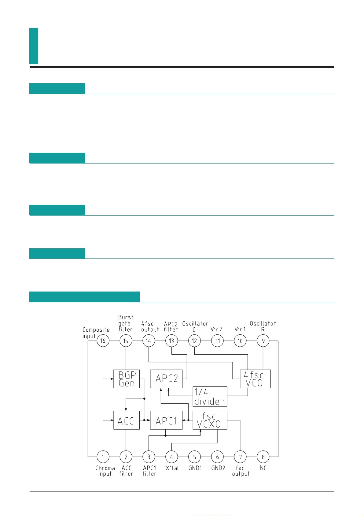
Outline
This IC generates a clock used for driving the CCD that configures a comb filter for Y/C separation, or for
sampling A/D and D/A converters that configure a digital comb filter.
It has a built-in subcarrier oscillator (3.58MHz or 4.43MHz) synchronized to the input chroma signal, and a
clock oscillator that is 4 times the latter. MM1093ND and NF are available for NTSC format, and MM1093PD
and PF for PAL format.
Features
1. Built-in fsc synchronized to input chroma signal and 4fsc oscillators
2. Reduced number of external parts due to 1 pin VCXO
3. +5V single power supply
Package
SOP-16A (MM1093NF, MM1093PF)
DIP-16B (MM1093ND, MM1093PD)
Applications
1. TV
2. VCR
Equivalent Circuit Diagram
Page 2
MITSUMI
4fsc Clock Generator MM1093
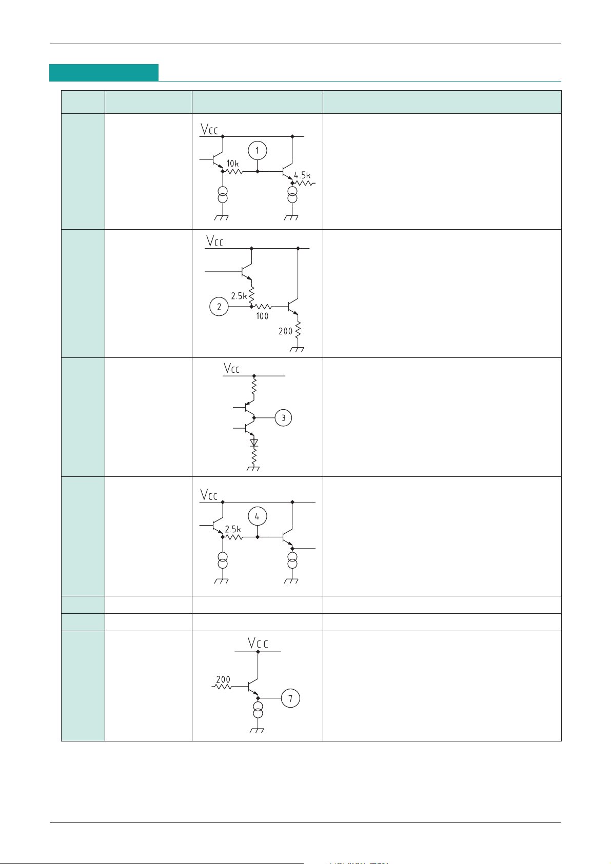
Pin Description
Pin no. Pin name Equivalent Circuit Diagram Pin Description
1 Chroma input
2 ACC filter
3 APC1 filter
Chroma signal input pin
ACC filter pin
fsc APC circuit filter pin
4 X'tal
5 GND1
6 GND2
7 fsc output
VCXO circuit X'tal pin
fsc GND pin
4fsc GND pin
Outputs subcarrier synchronized to input
chroma signal
NTSC : 3.579545MHz
PAL : 4.433619MHz
Page 3
MITSUMI
4fsc Clock Generator MM1093
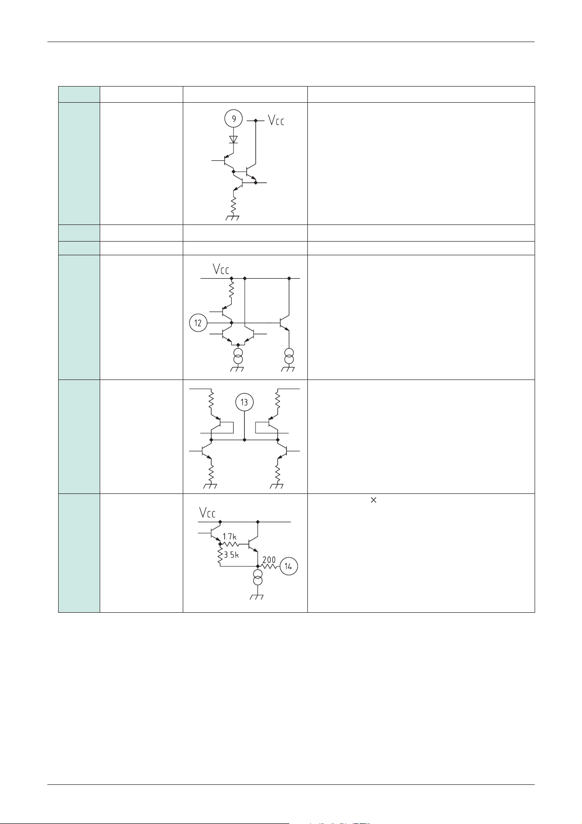
8 NC
9 Oscillator R
10 V
11 V
CC1
CC2
12 Oscillator C
NC pin
Connects to resistor that determines 4fsc VCO
free run frequency
fsc power supply pin
4fsc power supply in
Connects to capacitor that determines 4fsc
VCO free run frequency
13 APC2 filter
14 4fsc output
4fsc APC circuit filter pin
Outputs a 4 signal sychronized to input
chroma signal.
Page 4

MITSUMI
4fsc Clock Generator MM1093
15 Burst gate filter
16 Composite input
This pin creates burst gate pulse.
Composite signal input pin
Absolute Maximum Ratings
Item Symbol Ratings Units
Storage temperature T
Operating temperature T
Power supply voltage V
Allowable loss Pd 350 mW
(Ta=25°C)
STG
OPR
CC max. 7 V
-
40~+125 °C
-
20~+75 °C
Page 5

MITSUMI
1VP-P
VS
Hsync
4fsc Clock Generator MM1093
Electrical Characteristics
Item
Operating power supply voltage
Consumption current I
Sync separation circuit
Sync separation level V
PLL circuit
ACC input amplitude range V
APC1 frequency
acquisition range SG2 : 1V
VCO1 free run frequency deviation
fSC output level V
fSC output duty DO1
4fSC circuit
4fSC output level V
4fSC output DT D
fSC leakage Lfsc SG2 : 1V
Notes:
1 Sync separation level
*
Measure the level where SG1 input signal and TP3 output signal synchronize when 1V
sync signal level is raised from 0V.
(Except where noted otherwise, Ta=25°C, VCC=5.0V, SG1, SG2 : no signal, SW1 : A)
Symbol
Measurement
circuit
VCC VCC 4.7 5.0 5.3 V
CC
S TP3 SG1 : separate chroma signal 40 80 120 mV
IN TP1
C
f
f0
O1
O2 SG2 : 1VP-P staircase wave 0.8 1.0 1.2 VP-P
O2 TP3 SG2 : 1VP-P staircase wave 45 50 55 %
-
TP2 SG1 : separate chroma signal
Measurement conditions Min. Typ. Max. Units
SG2 : 1V
SG1 : separate chroma signal *2 *5
SG2 : 1V
SG1 : separate chroma signal
SG2 : 1V
SG1 : separate chroma signal
SG1 : separate chroma signal
SG1 : separate chroma signal
P-P staircase wave
SW1 : B
SG1 : sine wave 143mVP
P-P staircase wave
P-P staircase wave
P-P staircase wave
SW1 : B *5
SW1 : B
P-P staircase wave 50 dB
SW1 : B
*
5
*
4
5
*
5
*
24 32 mA
1
*
15 560
-
P
*
*
*
400 Hz
3
-
250 0 250 Hz
0.8 1.0 1.2 V
5
45 50 55 %
5
P-P staircase wave
mV
P-P
P-P
SG2 : 1V
2 ACC input amplitude range
*
Defined as separate chroma signal burst signal amplitude that can be input to chroma input.
3 APC1 frequency pull-in range
*
Defined as the smaller of the differences when input signal frequency is changed from high to f
low to fo when TP2 output is not synchronized to SG1 input signal and when it is synchronized.
4 VCO1 free run frequency deviation
*
Defined as the difference between TP2 output signal frequency and f
5 The standard for the separate chroma signal is burst signal 143mVP
*
P-P staircase wave
O.
-
P.
O and from
Page 6

MITSUMI
Measuring Circuit
4fsc Clock Generator MM1093
Notes:
1 NTSC : R=5.6k
*
PAL : 4.3k
2 Recommended crystal oscillator
*
Tokyo Dempa, TR-49 or equivalent
NTSC : 3.579545MHz
PAL : 4.433619MHz
3 Use part with precision within ±5% and temperature characteristic
*
CH.
4 R and C change according to board floating capacitance, etc.
*
Select R and C so that Pin 13 voltage is approximately 2V for VCO
lock. Also, C should be 4PF or higher, and R should be 3.3kΩ or
higher.
Page 7

MITSUMI
Application Circuits
4fsc Clock Generator MM1093
Notes:
1 NTSC : R=5.6k
*
PAL : R=4.3k
2 Recommended crystal oscillator
*
Tokyo Dempa, TR-49 or equivalent
NTSC : 3.579545MHz
PAL : 4.433619MHz
3 Use part with precision within ±5% and temperature characteristic
*
CH.
4 R and C change according to board floating capacitance, etc.
*
Select R and C so that Pin 13 voltage is approximately 2V for VCO
lock. Also, C should be 4PF or higher, and R should be 3.3kΩ or
higher.
5 BPF Reference circuit
*
 Loading...