

Page 1
MLX902xx Name of Sensor Rev Y.X 22/Aug/98 Page 1
MLX90721
Auto Shut Off Timer
MLX90721 Auto Shut Off Timer Page 1 Rev 1.0 22/Jun/00
Featur es an d Ben efits
Low cost – minimal external components
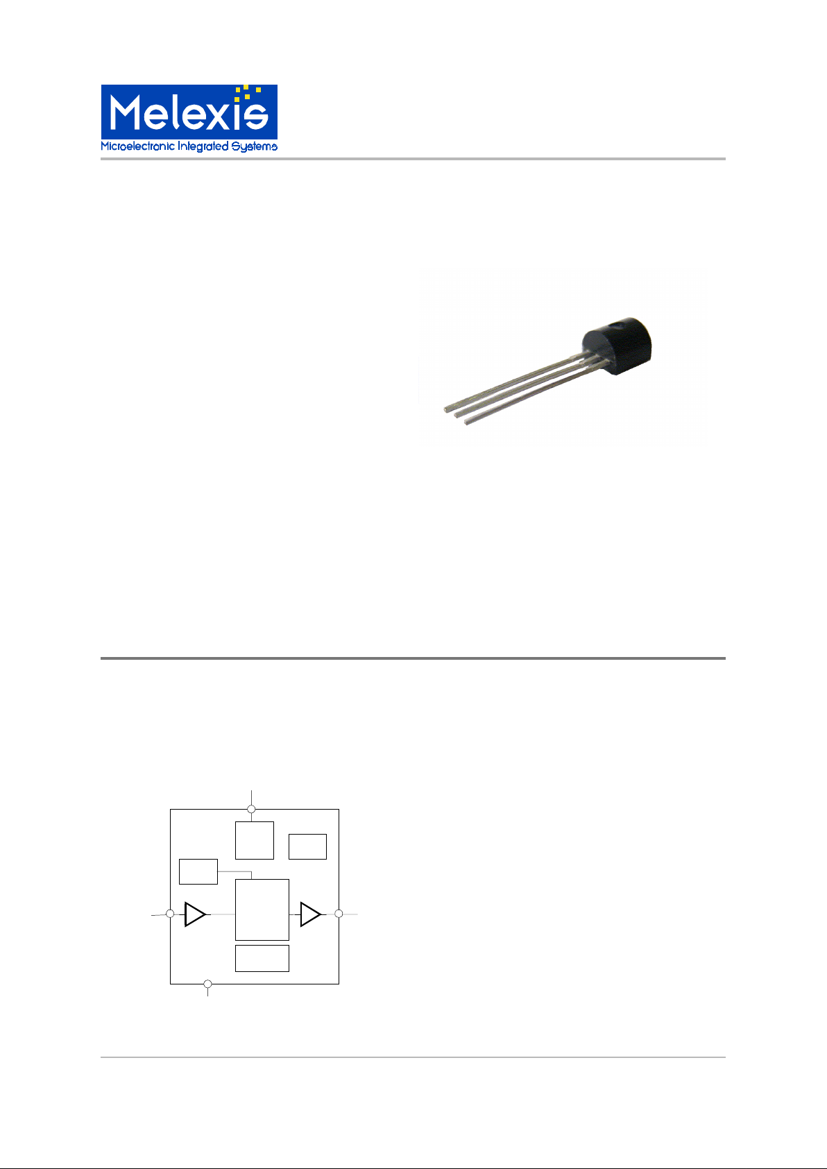
Small package ( to92 for the 3 pins version,
pdip8, psop8 or cob for the 4 pins version)
On chip calibrated timer
Drives different relay types, including low
cost 12V relays and most custom made
relays.
Low power consumption (low dissipation)
Applications
Househ ol d ap pl i an ces
Heater
Hand-dryer
Ordering Information
Part No. Temperature Suffix Package option Temperature Range
MLX90721 S TA -x 0C to 85C
MLX90721 S A -x 0C to 85C
MLX90721 S L -x 0C to 85C
The customer speci fi c option code is indicated with 1 character at the end of the ordering number.
For cob assembly, please contact Melexis directly.
Description
The chip is intended to be used for switching on and
off a mains powered device, with the added f eature
of automatic switch off after a well-defined amount of
time. Such device can replace conventional switches
in all appliances that might be left on inadvertently.
Besides saving energy, the main goal is to prevent
all hazards due to appliances left on unattended.
The chip can be used in its 3-pin version, where
applying the supply to the chi p does switching on.
In the 4-pin version switching on and off is done with
a single push-button.
As an alternative the fourth pin can also be used as
a reset pin, where the auto- shut-off tim e counter i s
reset when pushi ng this button.
The auto-shut-off time is mask programmable and
can be almost anyt hing between 2. 5 minutes and 32
hours. The duty cycle of the relay driver can also be
adjusted by mask to adapt to almost any kind of relay
construction.
Functional Diagram
Use Template :
block.vst
POR
Vreg
options
OSC
90721
logic
VDDA
VSS
BUT OUT
Page 2
MLX90721
Auto Shut Off Timer
MLX90721 Auto Shut Off Timer Page 2 Rev 1.0 22/Jun/00
General Description
The chip is intended to be used for switching on and
off a mains powered device, with the added f eature
of automatic switch off after a fixed amount of time.
Such device can replace conventional switches in all
appliances that might be left on inadvertently.
Besides saving energy, the main goal is to prevent
all hazards due to appliances left on unattended.
The c hi p is of f er ed i n a 3-pin v er s io n , w her e a p pl yi n g
the supply is switching the chip on. In its 4-pin
version, switching on and off is done with a single
push-button.
As an alternative the fourth pin can also be used as
a reset pin, where the auto- shut-off tim e counter i s
reset when pushi ng this button.
The chip application version (3 or 4 pins) and aut oshut-off time are mask programmable. The autoshut-off time can be almost any value between 2.5
minutes and 32 hours. The duty cycle of the relay
driver can also be adjusted by the same mask to
adapt to all types of relay cons truction.
Power-On-Reset.
The Po w er -O n - Res et of th e ASI C i s a com bi n at i on o f
a digi tal power-on-reset with hysteresi s DPOR, and
an analog APOR.
DPOR is used to initialize the logic on the chip.
The APOR is characterized by a low level – APL
signal and a high level – APH signal, which are
debounced as follows:
low level debouncing – appr ox. 25mS
high level debouncing – approx. 3.5mS
The digital signal APOR is a logic combination of the
debounced signal s APLd and APHd. APOR is set to
High when APHd = high and APOR i s reset to Low
when APLd = low.
A transition to the active state is indicated by the
digital signal
APOR=1
in c as e of ap p li c at i on 1 an d 2 ,
or
APOR=1
and
START=1
in case of application 3.
The result is that the transistor at the pin OUT is
activated after a delay time Td , and starts switching
ON and OFF with the specified frequency F1 and
duty cycle
DC1
.
The digital signal
APOR=0
immediately brings the
logi c back to the INACTIV E stat e, i.e. the out put is
disabled and the state of the digital output signal
from the start-stop/reset button (if present in the
particular application) is initialized to non-pressed
(released) state.
Button Input.
The Button Input can have three different functions,
which determine the three different applications:
APPL.1, APPL.2 and APPL.3. The function of the
input is defined by the options mask.
APPL.1-
No Function
. The BUT input is not used
and therefore not connected externally. BUT is an
internally pulled up digital input. In this case, the
transitions INACTIVE > ACTIVE state and vice
versa are defined only by the APOR signal.
APPL.2-
Auto Shut-OFF Time Reset
. The input
BUT can be connected to GND via an external
button. The input is an internally pulled up, active
Low, inverting digital input. In this case, the
transitions INACTIVE state > ACTIVE state and
vice versa are again defined only by the APOR
signal. Each time the button is pressed a Reset
signal is generated and the count down for the Auto
Shut-Off Time starts from 0 again.
The state of this input ( pressed or not ) is checked
each 3.5mS. The high level (button pressed) at the
digital output is debounced for approx. 3.5mS.
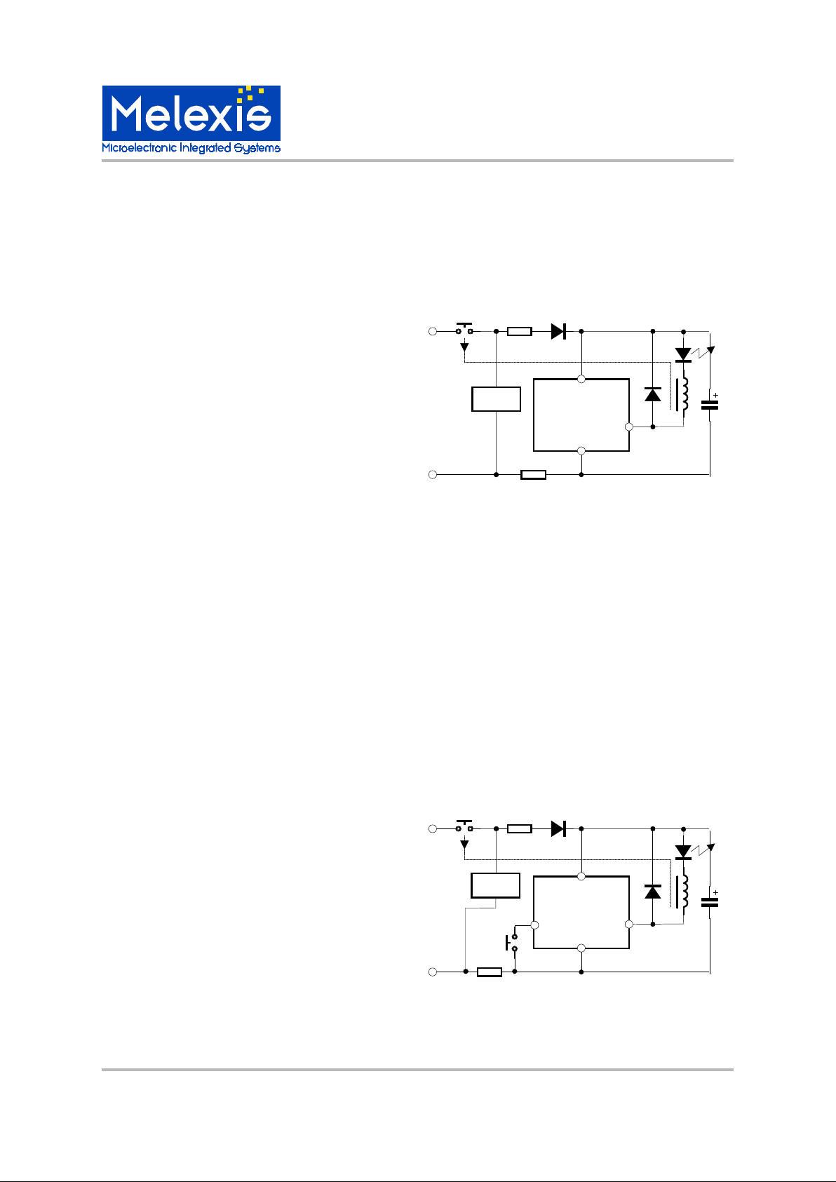
90721
LED (optional)
N
L
Load
VDD
GND
OUT
Appl.1 ASO without button
90721
LED (optional)
N
L
Load
VDD
GND
OUT
Appl.1 ASO with time reset button
BUT
Page 3
MLX902xx Name of Sensor Rev Y.X 22/Aug/98 Page 3
MLX90721
Auto Shut Off Timer
MLX90721 Auto Shut Off Timer Page 3 Rev 1.0 22/Jun/00
APPL.3-
Start/Stop Toggle Function
. The input BUT
is now an acti ve High, zero cross input wi th internal
pull down. The input is connected via a button and
external resistor to the mains. Each time this button
is pr essed , the i nter nal S TART si gnal toggl es and i n
com bi n ati o n wi t h th e A PO R si g nal it def i nes t he l o gi c
transitions in the following way:
APOR=1 and START=1 –> transition to ACTIVE
state
APOR=1 and START=0 –> transition to INACTIVE
state
APOR=0 – defines the INACTIVE state and
initialization of a start signal START= 0
The digital output of the BUT input is debounced as
follows:
High level debouncing (button pressed) – approx.
3.5mS
Low level debouncing (button released) – approx.
100mS
The first time the button is pressed after initialization
sets START=1. Once the logic has found that the
button is pressed, it has to detect a released button
in order to interpret correctly consecutive activations
of the button. Each next pressing toggles the START
signal.
Auto Shut-OFF Function.
When the ASIC is in the ACTIVE state and when the
delay period Td has elapsed, the output is activated
(wi th a wel l d efi ned dut y cycl e) for a pr edef i ned Au t o
Shut-OFF Time Ta. At the end of that period Ta, the
output is switched OFF, the ASIC is brought to the
INACTIVE state and the state of the digital output
si gnal fr om th e st art-st op/r eset b utton (if p resent ) is
initialized.
Internal Oscillator.
The ASIC has a calibrated free running, RC
oscillator, which is used to generate a frequency
and a duty cycle for the relay output, and the
different delays and Auto Shut-Off times.
Relay Output.
When the coil is not activated, the open drain
output transistor is in the OFF state constantly.
When the coil is activated, the output transistor
starts switching ON and OFF with the specified
frequency
F1
and with a duty cycle
DC1
.
Optionally, there could be doubled duty cycle
during the first few msec -
Tdub
. This option is
usef ul to provide th e extra energy needed for t he
mechanical movement when act ivating a relay.
Supply.
The c hip is di rectl y suppl ied fr om the mai ns, vi a a
diode and resistor. To limit the supply voltage
VDDA, a zener with a voltage of
Vzen
is
integrated.
To supply the analog and digital functions, an on
chip voltage regulator and the required biasing
ci r cuits are f oreseen.
Doubled Duty cycle
Mechanical relays normally need a higher magnetic field (and thus a higher coil current) to move
the c ontac t away from his norm al posi tion, t hen to
keep the contact in that position. Therefore it is
possible to increase t he current supplied to the coi l
during the first 6 msec. After activation of the output driver. This is done by doubling the duty cycle
which has been selected by mask option.
With a proper dimensioning of the external components the power consumption of the module can be
optimized in this way.
Test Mode
The test mode aims full verification of the above
specified logic functions and electrical characteristics, both on wafer and packaged device.
The test mode is defined under the following conditions:
V(O UT) = 0V for appr ox. 5m sec
. The ASIC enters
test mode when on pin
OUT
is detected a shortcircuit to GND. This detection is done after a digital
debouncing for a per iod of ~ 5mS, and the result is
latched and saved in a test status flip-flop.
When in test mode, pin
OUT
is used as an i nput
for the test clock sequence, as well as an output for
the IC reaction. This is achieved by appropriate
definition of input/output signal level s.
V(OUT) < 9V
. Thi s r es tri c t i on ai m s to mak e a cl ea r
distinction between normal mode operation, when
V(OUT)=
VDDA, and test mode. This feature also
ensures that if by mistake test mode is activated
during Normal Mode operation, and at the same
time on pin
OUT
is found a potential higher than
9V, follows immediate reset of test mode, and the
IC is brought back to normal mode.
Disclaimer
Melexis reserves the right to periodically make
modifications to product specifications. The information included herein is believed to be accurate
and reliable. However, Melexis assumes no responsibility for its use; nor for any infringements of
patents or other rights of third parties which may
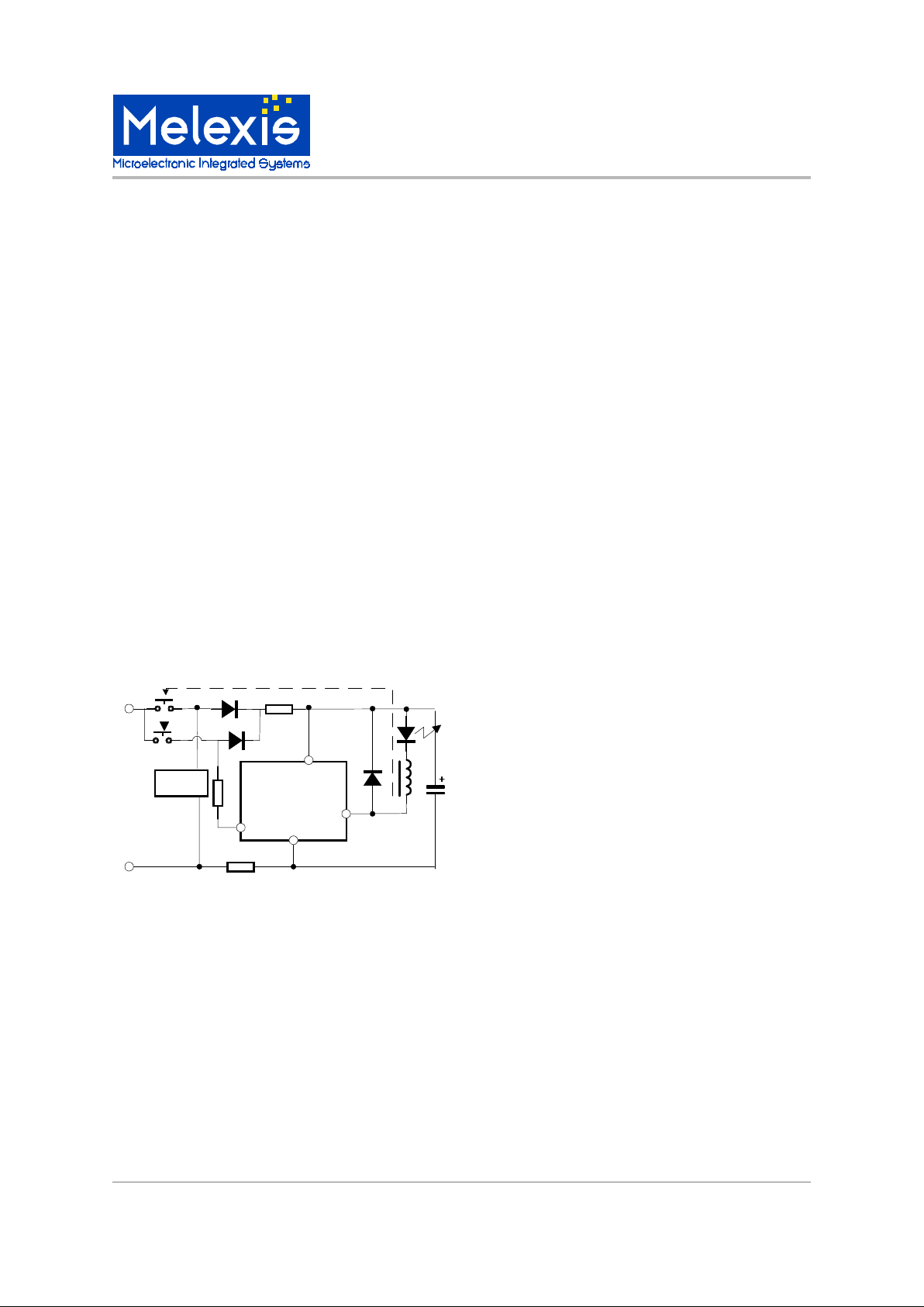
90721
LED (optional)
N
L
Load
VDD
GND
OUT
Appl.1 ASO with start/stop button
BUT
Page 4
MLX90721
Auto Shut Off Timer
MLX90721 Auto Shut Off Timer Page 4 Rev 1.0 22/Jun/00
MLX90721 Electrical Specifications
DC Operating Parameters TA = 0oC to 85oC
Operating Ranges
Parameter Symbol Test Conditions Min Typ Max Units
Max. junction temperature Tjm 125 °C
Ambient temperature Ta 0 85 °C
Supply Current
Parameter Symbol Test Conditions Min Typ Max Units
Supply current at
VDDA=48V
Idd1 VDDA=48V, OUT open BUT not active 170 270 370 µA
Supply current at
VDDA=55V
Idd2 VDDA=55V, OUT open BUT not active 200 300 400 µA
Integrated Zener
Parameter Symbol Test Conditions Min Typ Max Units
Zener voltage at VDDA Vzen 62 66 70 V
Maximum sink current Izm 10 mA
Power On Reset
Parameter Symbol Test Conditions Min Typ Max Units
DPOR high level Vdh 2.8 V
DPOR hysteresis Vdhys 0.9 V
APOR high level VAPH 32 42 V
APOR hysteresis VHYS 7 12 V
Page 5

MLX902xx Name of Sensor Rev Y.X 22/Aug/98 Page 5
MLX90721
Auto Shut Off Timer
MLX90721 Auto Shut Off Timer Page 5 Rev 1.0 22/Jun/00
Relay Driver Output
Parameter Symbol Test Conditions Min Typ Max Units
Maximum current in ON
state
Ion 50 mA
Output voltage in ON state Von Iout = 50mA 0.4 3 V
Leakage current in OFF
state
Ioff V(OUT)=Vzen 1 50 mA
Over voltage protection Vprot 90 V
Rise / fall time s Trf Iout = 25mA 0.7 1.0 1.3 µs
Frequency of the relay
driver
F1 21.8 kHz
Duty cycle of the relay
driver
DC1 See options Var. %
Internal Oscillator
Parameter Symbol Test Conditions Min Typ Max Units
Nominal frequency Fosc VDDA = 60V, Tamb 437 kHz
Frequency tolerance Df 20V < VDDA < 70V -6 6 %
Temp. coefficient of oscilla-
tor frequency
TCf T=0°-100°C 1000 ppm
Integrated Zener
Parameter Symbol Test Conditions Min Typ Max Units
Zener voltage at VDDA Vzen 62 66 70 V
Maximum sink current Izm 10 mA
Page 6

MLX90721
Auto Shut Off Timer
MLX90721 Auto Shut Off Timer Page 6 Rev 1.0 22/Jun/00
Button Input
Parameter Symbol Test Conditions Min Typ Max Units
Threshold voltage Vtr Valid for APPL.1 and APL.2 2.5 V
Threshold current Itr
Valid for APPL.3
+12 mA
Max. source current Im1 -350 mA
Max. sink current Im2 350 mA
Clamp voltage 1 Vc1 APPL.3; Ibut = +4mA 5 V
Clamp voltage 2 Vc2 APPL.3; Ibut = -4mA 0 V
Timings
Parameter Symbol Test Conditions Min Typ Max Units
Switch ON delay time Td 47 mS
Auto Shut-OFF time Ta See options
Increased Duty Cycle pe-
riod
Tdub In case this option is enabled 6 mS
Page 7

MLX902xx Name of Sensor Rev Y.X 22/Aug/98 Page 7
MLX90721
Auto Shut Off Timer
MLX90721 Auto Shut Off Timer Page 7 Rev 1.0 22/Jun/00
Duty Cycle and Auto Shut-OFF Options
The function of input BUT as well as the doubled duty cycle function can be define by mask option.
Also following options can be defined by mask option:
Parameter Symbol Test Conditions Min Typ Max Units
Relay Frequency Duty Cycle
DC In steps of 2.5% 5 37.5 %
Interval
0 – 1 H
2.5 5 7.5 10 12.5 15 17.5 20
22.5 25 30 35 37.5 40 45 50
52.5 min
1 – 2 H 1h 1h10m 1h15m 1h20m 1h30m 1h40m 1h45m
2 – 3 H 2h 2h20m 2h30m 2h40m
3 – 4 H 3h 3h20m 3h30m
4 – 5 H 4h 4h40m
5 – 6 H 5h 5h20m
6 – 7 H 6h 6h40m
7 – 9 H 7h 8h
9 – 10 H 9h 9h20m
10 – 11 H 10h 10h40
12 – 32 H 12h 14h 16h 20h 24h 28h 32h
AUTO SHUT-OFF TIMES
ESD Precautions
Electronic sem iconductor products are sensitive to
Electro Static Discharge (ESD).
Always observe Electro Static Discharge control
procedures whenever handling semiconductor
products.
Pin Name Type Description
1 VDDA Input supply
2 GND Input ground
3 OUT output relay driver output
4 (opt.) BUT input Button input
Pinout
Standard package f or the 3 pins version is a 3-pin
TO 92 package, and PDIP8 or PSOP8 for the 4
pins version.
Page 8

MLX90721
Auto Shut Off Timer
MLX90721 Auto Shut Off Timer Page 8 Rev 1.0 22/Jun/00
“A” Package Dimensions
9.02
10.16
Min
Max
18.67
19.68
18.67
19.68
22.35
23.67
24.89
26.92
31.24
32.51
0.20
0.38
2.54
BSC
1.1
5
1.7
7
0.35
0.55
0.39
Min
Dimension 8 Leads 16 Leads 18 Leads 20 Leads14 Leads 24 Leads
A
6.10
7.11
5.33
MAX
2.93
4.06
7.62
BSC
10.92
Max
A
Notes:
1-All measurements in mm
2-Body dimensions do not include mold
flash or protrusion - not to exceed
0.15mm
Page 9

MLX902xx Name of Sensor Rev Y.X 22/Aug/98 Page 9
MLX90721
Auto Shut Off Timer
MLX90721 Auto Shut Off Timer Page 9 Rev 1.0 22/Jun/00
“L” Package Dimensions
0.40
1.27
0o to 8
o
2.35
2.65
0.010 min.
0.33
0.51
A
Dimension 8 Leads 14 Leads
A
4.80
5.00
Min
Max
8.55
8.75
16 Leads
9.80
10.00
3.80
4.00
5.80
6.20
1.27
Notes:
1-All nominal measurements in millimeters
2-Body dimensions do not include mold flash
or protrusion - not to exceed
0.15mm
Page 10

MLX90721
Auto Shut Off Timer
MLX90721 Auto Shut Off Timer Page 10 Rev 1.0 22/Jun/00
“TA” Package Dimensions
Dimensions in millimeters Di m ensions in inches
MIN NOM MAX MIN NOM MAX
A 3.45 3.56 3.66 0.136 0.140 0.144
A1 1.22 1.30 1.37 0.048 0.051 0.054
b - 0.38 - - 0.015 C - 0.38 - - 0.015 D 4.27 4.52 4.78 0.168 0.178 0.188
D1 4.14 4.29 4.45 0.163 0.169 0.175
E 4.32 4.57 4.83 0.170 0.180 0.190
L 12.98 13.49 14.00 0.511 0.531 0.551
e - 1.27 - - 0.050 q - 5º - - 5º q - 5º - - 5º -
symbols
Note: All dimensions in inches.
Page 11

MLX902xx Name of Sensor Rev Y.X 22/Aug/98 Page 11
MLX90721
Auto Shut Off Timer
MLX90721 Auto Shut Off Timer Page 11 Rev 1.0 22/Jun/00
For the lat est ver s i on of this docu m ent,
Go to our website at:
www.melexis.com
Or for additional inf or m ati on
contact Melexis Direct:
USA
Melexis Inc.
41 Locke Road, Concord, NH 03301
Phone: +1 603 223 2362 Fax: +1 603 223 9614
E-mail: sales_usa@melexis.com
United Kingdom
Silicon Concepts
PCB Lynchborough Road, Hampshire GU30 7SB, United Kingdom
Phone: +44 1428 751 617 Fax: +44 1428 751 603
E-mail: sale s_ u k@ me lexis.com
Germany
Am Seestern 8, 40547 Düsseldorf, Germany
Phone: +49 211 5360212 Fax: +49 211 5360250
E-mail: sales_de@melexis.com
France
Melexis France
Tour Arago, 5 rue Bellini, 92806 Puteaux-La-Défense, France.
Phone: +33 1 47 78 11 34 Fax: +33 1 47 78 06 35
E-mail: sales_france@me lexis.com
Italy
Dimacred IRL
Via Papa Giovanni XXIII no. 25, 20046 Biassono, Italy
Phone: +39 039 249 4856 Fax: +39 039 491773
E-mail: sale s_italy@melex is. co m
Japan
Satori Electric Co., LTD
1-14-10 Shiba, Minato-Ku, Tokyo, Japan
Phone: +81 3 3452 7171 Fax: +81 3 3769 2197
E-mail: sales_japan@melexis.com
Taiwan
Beechwood Int’l Taiwan Co.
Room 8, 17F, No. 189, Taipei, Taiwan
Phone: +886 2 2739 3322 Fax: +886 2 2739 3090
E-mail: sales_taiwan@ melexis.com
 Loading...