

Page 1
MLX902xx Name of Sensor Rev Y.X 22/Aug/98 Page 1
MLX9 0719
General purpos e timer
MLX90719 General purpose timer Page 1 Rev 1.0 30/Jul/00
Featur es an d Be n efi ts
1µm CMOS technology
MLX8 core with 8 accumulators, 80 b
y
tes RAM and 6K ROM
1 hi
g
h voltage input (detection of mains-active)
Zero-crossin
g
detection input to detect the 50/60Hz
7 standard inputs of which 2 can be used as comparator inputs and 2 can be confi
g
ured as
open-collector o utp uts .
15 confi
g
urable LCD outputs (segment/backplane)
3 rela
y
drivers which can also be used to drive a triac or LED’s without the need for external resistors.
Buzzer driver with pro
g
ramm able frequency
On-chip 4MHz oscillator, cr
y
stal oscillator and low power RC oscillator
Low power mo de
(
battery or decoupling capacitor)
Hi
g
h supply voltage eliminates the need for high power resistors
Batter
y
backup
On-chip watchdo
g
Applications
24 hour timer for cooker applications, coffee maker, ...
Ordering Information
Part No. Temperature Suffix Package version Temperature Range
MLX90719 S LS -x 0C to 85C
The c ustom er sp ecifi c ver sion c ode
(
defining the RO M conten t) is i ndi cat ed wit h 1 cha rac ter at th e en d of th e
orderin
g
number.
Description
The ASIC consists of a dedicated microcontroller
combined with on-chip analo
g
and digital blocks,
which can be confi
g
ured to a great extend. This
makes it ideal to adapt it to different applications b
y
means of an update in the software. The number of
external components for the electronic module is
minimized. A t
y
pical application mainly consists of
the MLX90719 ASIC, a number of command buttons,
a LCD, a rela
y
, some LED’s and a buzzer.
The number of buttons and their function can be
freel
y
chosen. The configuration of the LCD, the
number of backplanes and its pinout is also under
software control. Three outputs are available for a
rela
y
and LED’s.
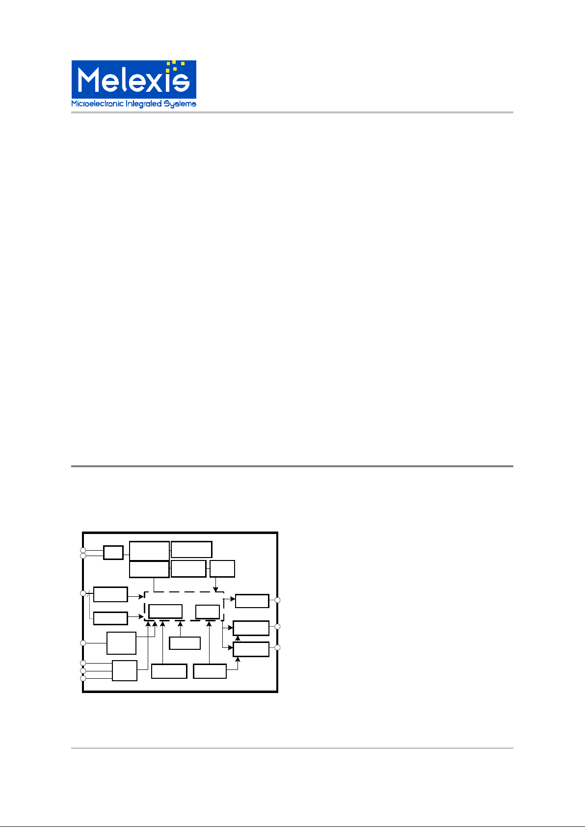
Functional Diagram
MLX90719
LX11
Interrupt
controller
RAM
1 x comp
CounterWatchdo
g
XT1
XT2
IN 1-8
ZCD
VDD4
BAT
VSS
LCD 1-15
OUT A,B,C
BUZ
17bit timer
Controller
125kHz
oscillator
4MHz
PLL
LC
oscillator
POR
8 x input
Vre
g
Xtal
LCD
Output
A, B, C
Buzzer
Zero
cross
Page 2

MLX9 0719
General purpos e timer
MLX90719 General purpose timer Page 2 Rev 1.0 30/Jul/00
General description
The MLX90719 is an ASIC which is ideally suited
for timing control application, low cost as well as
high end, such as clocks in coffee machines, cookers, baking eq uipm ent,...
The ASIC consists of a dedicated microcontroller
combined with on-chip analog and digital blocks,
which can be configured to a great extend. This
makes it ideal to adapt it to different applications by
means of an update in the software. The number of
external components for the electronic module is
minimized. A typical application mainly consists of
the MLX90719 ASIC, a number of command buttons, a LCD, a relay, some LED’s and a buzzer.
The number of buttons and their function can be
freely chosen. The configuration of the LCD, the
number of backplanes and its pinout is also under
soft war e contr ol. Thr ee out puts ar e avail able f or a
relay and LED’s.
Main functions:
General-purpose timer chip based on the 8-bit
LX11 core, including 80 bytes RAM and 6 Kbytes
ROM.
Programming of the ROM and selection of all other
options is done with one mask.
An interrupt controller guarantees exact timings
and a clean refresh rate of the LCD.
High supply voltage eliminates the need for high
power resistors.
6 digital inputs and 2 I/O pins (function is under
software control).
1 comparator (uses 2 of the digital inputs) which
can be used for analog measurements.
3 hig h cur rent out put dri ver s. Th ey are s uita bl e for
driving low cost 12V relays, but other types can
also be used. They can also be used to drive triac
or LED’s without the need for external resistors.
1 bu zzer ou t pu t fo r piezo el ec t r ic b u zzer s, w it h pr o grammable frequency.
The LCD interface consists of 15 outputs, each of
them can be con figured as backpl ane or segm ent
driver.
The time base for the clock function is derived either f r om t he m ains fr eq uen c y o r f r om a cr y st a l o s cillator.
The clock frequency for the microcontroller, relay
drivers and buzzer output is derived from an on
chip oscillator, which is calibrated under software
control.
For applications that are disconnected from the
mains for longer times, a battery backup can be
foreseen, so that the module always keeps track of
the time.
For short mains interruptions (up to 5 minutes), the
energy in a decoupling capacitor can be used to
keep track of the time.
An on-chip watchdog ensures the functioning of the
chip under all environmental conditions.
The package size can be adapted to the number of
used pins (non-used I/O’s do not need to be
bonded).
Page 3

MLX902xx Name of Sensor Rev Y.X 22/Aug/98 Page 3
MLX9 0719
General purpos e timer
MLX90719 General purpose timer Page 3 Rev 1.0 30/Jul/00
MLX90719 Electrical Specifications
DC Operating Parameters T
A
= 0oC to 85
o
C, VDD = 60V (unless otherwise specified)
Parameter
Symbol
Test Conditions
Min Typ Max Units
Ambient temperature
Tamb
0
85 °C
Maximum chip temperature
Tic
150 °C Maximum allowed source
supply current
Idd4m
Drivers off = all the current flows in the chip
6 mA
Analog features
Power supply
The MLX90719 suppl
y
pin (VDD4) must be connected
b
y
external series resistor and rectifier diode to the
mains. An internal Zener function limits the volta
g
e at
VDD4 to 70-80V. For proper operation, a decouplin
g
capacitor needs to be connected between VDD4 and
VSS
(
see figure 1).
90719
Vdd4
Vss
line
R1
R2
C
6k*
6k*
22uF*
*for information onl
y
Page 4
MLX9 0719
General purpos e timer
MLX90719 General purpose timer Page 4 Rev 1.0 30/Jul/00
The MLX90719 has several internal supply lines for both analog and digital blocks:
Parameter
Symbol
Test Conditions
Min Typ Max Units
Voltage applied at the supply pin
Vdd4 Idd4 = 5mA
DRAINB = Vss
63 73 77 V
Internal buzzer driver supply
Vbuz Option OBZ3 active
20 V
Internal 11V supply
Vdd2 10 15 12 V
Internal 5V for main oscillator
Vdd1 4.5 5.0 5.5 V Internal 5V for digital
Vdd Normal mode
4.0 5.0 6.0 V Low power mode
2.7
LCD driver supply
Vlcd Option OLCD1 active
3.0 V
Option OLCD2 active
3.25 V
Option OLCD3 active
3.5 V
Option OLCD4 active
3.75 V
Option OLCD5 active
4 V
Option OLCD6 active
4.25 V
Option OLCD7 active
4.5 V
Option OLCD8 active
4.75 V
Option OLCD9 active
5 V
Option OLCD10 active
5.25 V
Option OLCD11 active
5.5 V
Option OLCD12 active
5.75 V
Option OLCD13 active
6 V
Option OLCD14 active
6.25 V
1Vlcd/3
Vlcd1
Of Vlcd
30 33 36 %
2Vlcd/3
Vlcd2
Of Vlcd
64 67 70 % Idd4 For Vdd4<Vaporl (LPM)
3
uA For Vdd4 = 73V
5 mA
Voltage of backup battery
Vbat
2.7 3 3.3 V Supply for external circuitry
Vext At Iext = 2mA
3.9 5 V
Page 5
MLX902xx Name of Sensor Rev Y.X 22/Aug/98 Page 5
MLX9 0719
General purpos e timer
MLX90719 General purpose timer Page 5 Rev 1.0 30/Jul/00
Parameter
Symbol
Test Conditions
Min Typ Max Units
High level threshold
Vdporh
3.4 V Low level threshold
Vdporl
2.2
2.6 V Hysteresis
Vdphyst
0.3 V
Notes:
The power on reset does not reset the s
y
stem when en tering low power mode with battery (Vdporl<Vbat).
The power on reset resets the s
y
stem if the RAM data may be corrupt due to undervoltage (Vdporl>RAM data
retention volta
ge)
.
Analog Power-On Reset
The MLX90719 includes a high voltage power-on reset that watches on VDD3.
This block has two outputs APORL and APORH:
APORL = 1 when VDD3 > Vaporl
APORH = 1 when VDD3 > Vaporh
(
see table 4)
The states of APORH and APORL define the operation mode of the chip
(
see s ecti ons “S leep m anager” and
“Interrupt controller”
)
.
In low power mode the analo
g
power on reset operates in strobe mode. It is only enabled a few microseconds at
each risin
g
edge of th e signal ASTR generated by the digital core.
When Vdd3 > Vapo r l the ci rcuit
g
oes out of strobe mode.
Parameter
Symbol
Test Conditions
Min Typ Max Units
High level threshold
Vaporh
65 V Low level threshold
Vaporl
50 V Hysteresis
Vaphyst
10 V Strobe frequency
Fastr Slow rate of Vdd3>200V/s
25 Hz
Low power mode (LPM)
In low power mode (when the mains hav e been dis connec ted from the application) all supply lin es ar e di s abled
except VDD, which is
g
enera ted by a low co nsum ing regulator. The current is taken from the external decou-
plin
g
capa cit or of V DD4 or f rom a ba ck up ba tt ery connected to pin BAT. This depends on the type of applica-
tion defined b
y
the mask option OXBAT implem ented within the chip:
OXBAT = 1 for application with batter
y
and crystal.
OXBAT = 0 for applications without batter
y
or crystal.
LCD operating voltage
The LCD operating voltage can have14 different values and can be chosen by mask options.
Supply for external components
If the mask option OVEXT is set the MLX90719 can supply some external circuitry from the internal Vdd1
throu
g
h pin IN5B (which can not be used as input anymore).
Power On Reset
This module ensures a correct start of the MLX90719 logic.
The reset si
g
nal (DPORB) rises when VDD>Vdporh and falls when VDD<Vdporl
Page 6
MLX9 0719
General purpos e timer
MLX90719 General purpose timer Page 6 Rev 1.0 30/Jul/00
Zero crossing detector
The MLX90719 includes a zero crossing detector on pin ZCD. This detector contains two comparators with hysteresis. The first comparator has negative thresholds and the second one has positive thresholds (see table 5).
Outputs ZOUT1 and ZOUT2 of those comparators are changing as follows:
ZOUT1 rises wh en Vmains>Vz1h
ZOUT1 fal ls when Vmains<V z1l
ZOUT2 rises wh en Vmains>Vz2h
ZOUT2 fal ls when Vmains<V z2l
A mask option defines the levels of those thresholds. Low levels (+/- 5V, option OZCD = 0) are suitable for zero
crossing detection and high levels (+/- 20V, option OZCD = 1) for frequency detection with a better noise immunity.
A 1MΩ resistor must be connected between pin ZCD and the mains.
Parameter
Symbol
Test Conditions
Min Typ Max Units
High level threshold 1
Vz1h Rzcd = 1Mohm
-5 V Rzc d = 1Mohm, OZCD = 1
-5 V Low level threshold 1
Vz1l Rzcd = 1Mohm
-9 V Rzcd = 1Mohm, OZCD = 1
-29 V High level threshold 2
Vz2h Rzcd = 1Mohm
9 V
Rzcd = 1Mohm, OZCD = 1
29 V
Low level threshold 2
Vz2l Rzcd = 1Mohm
5 V
Rzcd = 1Mohm, OZCD = 1
5 V
External resistor
Rzcd Vline = 230VAC typical
0.8 1 1.2 Mohm
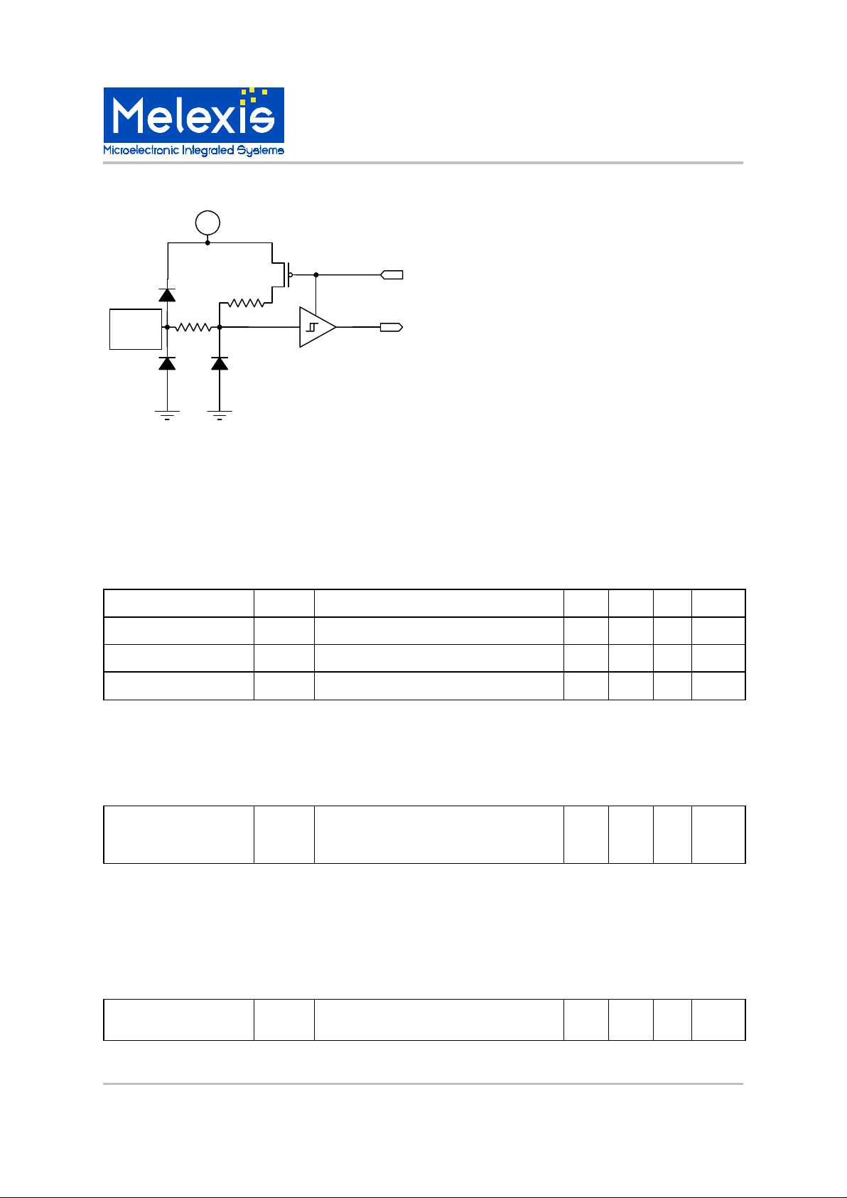
Low voltage inputs
The MLX90719 has 7 CMOS Schmitt trigger inputs with internal pull-up.
Note:
the input signals are inverted in the digital core so these inputs are active low.
Signal ENINB (active at 0) enables the pull-up current flowing through external pad to VSS if the input is pushed
to VSS. When ENINB=1 (input disabled), DINxB = 1.
The programmer must enable inputs by setting bit ENIN of P7 at least 5us before reading the input port P3 (see
section “I/O ports”). The debouncing of inputs must be done by software.
Parameter
Symbol
Test Conditions
Min Typ Max Units
Pull-up current
Ipu1 Input to Vss
40 70
100 uA Low level threshold
Vthinl
30 %Vdd
High level threshold
Vthinh
70 %Vdd
Hysteresis
Vhystin
5 %Vdd
Multipurpose inputs:
Inp uts 3 and 6 ca n be used al so as pul l-dow n output s: the pul l down tr ansis tors ar e turn ed on by sett ing bit s
PD3 and PD6 of P6 (see section ”I/O ports”).
Inputs 1, 2 and 4 are used by the on-chip comparator (see section “comparator”)
Input 5 can be tur n ed into sup ply for external cir cuitry by mask option OVEXT (see “Power s u p pl y ”).
Page 7
MLX902xx Name of Sensor Rev Y.X 22/Aug/98 Page 7
MLX9 0719
General purpos e timer
MLX90719 General purpose timer Page 7 Rev 1.0 30/Jul/00
High voltage input
The MLX90719 has an eighth input that can be used either as a standard input (as described above) or as an
hi
g
h volt age input to detect the mains via an external resistor. The high voltage mode is enabled if mask option
OIN7 is set.
Output DIN7B of this detector is hi
g
h when Vmains>Vthinh2 and low when Vmains<Vthinl2.
Note:
si
g
nal DIN7B is inverted whiti n the digital core.
Parameter
Symbol
Test Conditions
Min Typ Max Units
Pull-down current
Ipd2 12 uA
Low level threshold
Vthinl2
Rin = 1Mohm
6.9 V
High level threshold
Vthinh2
Rin = 1Mohm
12.3 V
External resistor
Rin
0.8 1 1.2 Mohm
Main oscillator
The MLX90719 contains a 4Mhz on-chip oscillator.
In low power mode this oscillator is turned off.
Parameter
Symbol
Test Conditions
Min Typ Max Units
Master frequency of the
main oscillator (signal
CKM)
Fckm
Over full temp. and supply range
2.4 4.0 5.6 MHz
Low power crystal oscillator
In case of applications with battery and crystal (OXBAT = 1) the MLX90719 uses a low power crystal osci ll ato r
as time reference for both normal and low power mode.
This oscillator re
q
uires a standard 32kHz crystal connected between pin XTAL1 and pin XTAL2.
No external capacitor is re
q
uired for proper operation.
Parameter
Symbol
Test Conditions
Min Typ Max Units
Master frequency of the
crystal oscillator
Fckx Over full temp. and supply range
32768
Hz
Note:
This oscillator is disabled if OXBAT = 0.
VDD
INxB
ENINB
DINxB
Page 8
MLX9 0719
General purpos e timer
MLX90719 General purpose timer Page 8 Rev 1.0 30/Jul/00
Low power RC oscillator
In case of applications without battery or crystal (OXBAT = 0) the MLX90719 uses an on-chip low power RC oscillator to count time during a few minutes after the mains has been disconnected (low power mode).
Parameter
Symbol
Test Conditions
Min Typ Max Units
Master frequency of the
low power RC oscillator
Fckl Over full temp. and supply range
1.0 2.5 5 kHz
Notes:
As the CPU must calibrate it in normal mode, the low power oscillator is running continuously.
The low power RC oscillator is disabled if OXBAT = 1.
LCD outputs
The MLX90719 has 15 configurable LCD outputs able to drive either a backplane or a segment by mask option:
OLCDx = 0 => segment
OLCDx = 1 => backplane
The LCD voltages are defined according to bits LCDx and CKLCD written in P3 and P4 (see section “I/O
ports”). With Vcdl1 and Vlcd2 being respectively 1/3Vlcd and 2/3Vlcd, the MLX90719 is suitable for LCD having
1, 2, 3 or 4 backplanes.
Parameter
Symbol
Test Conditions
Min Typ Max Units
Output impedance
Rolcd
All cases
20
kohm
OLCDx
LCDx
CKLCD
OUT 0 0 0 Vlcd1
0 0 1
Vlcd2
0 1 0
Vlcd 0 1 1 Vss 1 0 0 Vlcd2
1 0 1
Vlcd1
1 1 0
Vss 1 1 1 Vlcd
Relay drivers
The MLX90719 includes 3 pull-down power outputs A, B, and C able to drive relays, triacs or LED’s.
The gates of the drivers are controlled respectively by signals POUTA, POUTB and POUTC generated by the
digital core (see section “PWM generator”).
Each driver has its source and its drain connected to a pad (DRAINx and SOURCEx) except driver C of which
the source is connected to the ground. This allows a series connection of the drivers. In such a configuration
the current flowing through the relay is used to feed the LED’s.
Internal current generator
In a ppli cati ons b ased on th e foll owi ng sc hemati c, w here t he LE D(‘ s) may have t o be dr iven when the r elay is
off, an internal current peak generator can be activated to supply the LED’s through pin SourceA. This function
is enabled by bit INTCUR of P5 (see section “I/O ports”). When INTCUR is set the current generator is activated like a relay by signal PINT at frequenc y Fpwm and at 14.3% duty c ycle (see “PWM generator”).
Note:
If the application has no relay, this feature allows the MLX90719 to drive 2 LED’s without any external
resistors.
Page 9

MLX902xx Name of Sensor Rev Y.X 22/Aug/98 Page 9
MLX9 0719
General purpos e timer
MLX90719 General purpose timer Page 9 Rev 1.0 30/Jul/00
Parameter
Symbol
Test Conditions
Min Typ Max Units
Ron of driver A
RonA
Source A pushed to VSS
10 30 W Ron of driver B
RonB
Source B pushed to VSS
10 30 W Ron of driver C
RonC
10 30 W
Voltage on pin DrainA
Vda 85 V
Voltage on pin DrainB
Vdb 85 V
Voltage on pin DrainC
Vdc 85 V
Voltage on pin SourceA
Vsa 8 V
Voltage on pin SourceB
Vsb 4 V
Rising edge duration, all
drivers
Tr
Load = 5k from VDD4 = 70V
1 us
Falling edge duration, all
drivers
Tf
Load = 5k from VDD4 = 70V
1 us
VDD4
90719
DrainA
SourceA
DrainB
SourceB
DrainC
RELAY
LED1
LED2
8V
Current
gen.
PINT
Page 10

MLX9 0719
General purpos e timer
MLX90719 General purpose timer Page 10 Rev 1.0 30/Jul/00
Buzzer driver
The MLX90719 includes a piezo buzzer driver.
The push-pull output stage of this driver operates at 15V. An internal resistor between the output pin and the
pus h-pul l stage protects the chip against reverse piezo effect.
Parameter
Symbol
Test Conditions
Min Typ Max Units
Output impedance
Rob
100 300 600 ohm Maximum output frequency
Fbuzm
8 kHz
Comparator
The MLX90719 includes a multi-purpose comparator.
Setting bit ECOMP of P3 (see section “I/O ports”) enables this comparator. Inputs IN1B and IN2B become respectively the positive and negative inputs of the comparator and IN4B becomes its output via a tri-state buffer.
To reduce the number of external components in applications using the comparator, a resistive bridge and a
feed back resistor (both internal) can be connected on the positive input of the comparator by mask option
OCOMP.
Notes:
Some logic in the digital core ensures that ENIN12B and ENIN4B = 1 when ECOMP = 1.
When ECOMP = 0 the comparator output is fixed to “1”.
A programmable prescaler has been implemented to allow frequency measurement at the output of the comparator (line IN4B). The status of bits CM0 and CM1 of P3 define the prescale ratio as described in table 15:
electrical c haracteristic s of the compa r ator .
Parameter
Symbol
Test Conditions
Min Typ Max Units
Common mode range
Vcm 20 80 %Vdd
Offset
Vcoff -30 30 mV
CM1 CM0 Divide ratio
0 0
Prescaler bypassed
0 1
/16 1 0 /32 1 1 /64
Page 11

MLX902xx Name of Sensor Rev Y.X 22/Aug/98 Page 11
MLX9 0719
General purpos e timer
MLX90719 General purpose timer Page 11 Rev 1.0 30/Jul/00
Tri state
COMP
R
R
OCOMP
ECOMP
A
SA
CKM*
CTST*
(* reserved for test)
R
VDD
IN1B
ENIN12B
VDD
IN2B
ENIN12B
VDD
IN4B
ENIN4B
DIN1B
DIN4B
DIN2B
Page 12

MLX9 0719
General purpos e timer
MLX90719 General purpose timer Page 12 Rev 1.0 30/Jul/00
Digital fe at ur es
I/O ports
The MLX90719 has 9 port addresses. Read and write instructions to the same address do not access to the
same port:
Note: * = reserved for test.
Note: * = reserved for test.
Out Description
Msb Lsb
P0 Timer compare low
TCP7 TCP6 TCP5 TCP4 TCP3 TCP2 TCP1 TCP0 P1 Timer compare high
TCP15
TCP14
TCP13
TCP12
TCP11
TCP10
TCP9 TCP8 P2 Timer ctrl, comparator
CM1 CM0 ECOMP
TRST COUNT
EN24H
MUX1
MUX0
P3
LCD port
LCD8 LCD9 LCD10
LCD11
LCD12
LCD13
LCD14
LCD15
P4
LCD port
CKLCDB
LCD1 LCD2 LCD3 LCD4 LCD5 LCD6 LCD7 P5 Power outputs
Not used
INTCUR
PC1 PC0 PB1 PB0 PA1 PA0 P6 PWM frequency adjust
PD6 PD3 DIV5 DIV4 DIV3 DIV2 DIV1 DIV0 P7 IT control, sleep, wdog
PWD RSTWD
FLAG ENIN RFHIT
ETIMI ECLKI
ESUPI
P8
Sound, test
CTST*
DTST*
MTST*
LTST*
SOUND3
SOUND2
SOUND1
SOUND0
in Description
Msb Lsb
P0 Timer low
T7 T6 T5 T4 T3 T2 T1 T0 P1
Timer high
T15 T14 T13 T12 T11 T10 T9 T8 P2 Timer msb, test
BATB*
X* X* X* X* X* X*
T16 P3 Chip inputs
IN7 IN6 IN5 IN4 IN3 IN2 IN1 IN0 P4 Not used
X P5
Not used
X
P6 Not used
X
P7 IT handler, flag
ZCD 0 FLAG 0 0 PTIMI PCLKI
PSUPI
P8 Not used
X
Page 13

MLX902xx Name of Sensor Rev Y.X 22/Aug/98 Page 13
MLX9 0719
General purpos e timer
MLX90719 General purpose timer Page 13 Rev 1.0 30/Jul/00
Sleep manager and watch dog
At power-on-reset the MLX90719 is in low power mode (PWD = 1).
When VDD3 reaches 65V
(
APORH = 1) PWD is reset and the main oscillator starts. To ensure a correct start of
the analo
g
blocks, the CPU is kept in reset status for 215 mai n clock p ulses (typically 8.2ms).
Once the microcontroller is workin
g
a watchdog circ uitry wil l generate a system r eset i f the user pr ogram fails to
reset the watchdo
g
counter. The watchdog delay is given by:
Twd = 57344 x 1/Fckm
(
= 14ms if Fckm = 4MHz)
The watchdo
g
counter is reset each time a 1 is written on bit RSTWD of P7.
To distin
g
uis h a wake-up after pow er-on reset and a wak e-up after low power mode, one can read the status of
bit FLAG
(
read/write bit in P7). This will be 0 after power on reset and 1 after low power mode if FLAG has been
set durin
g
normal mode.
The low power mode is set b
y
bit PWD of P7. Since the main oscillator stops as soon as PWD = 1, setting bit
PWD must be the last instruction of the suppl
y
interrupt subroutine (see interrupt controller).
Debouncing
A debounce circuit eliminates positive spikes on line APORH to avoid unexpected wake-up due to disturbances. The debounce time
(
tdaporh) depends on OXBAT.
If OXBAT = 1 it derives from the cr
y
stal oscillator frequency and:
7.8ms < tdaporh < 11.7ms
If OXBAT = 0 it derives from the low power RC oscillator fre
q
uency and:
3.2ms < tdaporl < 24ms
Timer
The MLX90719 includes a 17-bit timer preceded by a 15-bi t pr esc a l er . T h e clo c k of th e ti mer can b e ta k en fr om
four different sources defined b
y
the bits MUX0 and MUX1 of P2:
The batter
y
and crystal option (OXBAT) defines which clock is connected to the prescaler input:
If OXBAT =1: the cr
y
stal oscillator output (CKX) drives the prescaler input
If OXBAT = 0: the low power RC oscillator output
(
CKL) drives the prescaler input.
Control bits
(P2)
:
EN24H = 1 enables the 24h mode
(
see below).
COUNT = 1 enables the counter
TRST = 1 resets the counter and the prescaler.
Normal operation
In normal mode the timer is used as a free-runnin
g
counter on CK125K. It can be read at any time without stop.
An interrupt is
g
enerated when the value of th e timer reaches the value of t he timer compare w r itt en in P1-P0.
Low power mode if crystal oscillator (OXBAT = 1)
In this mode the clock of the timer must be connected to the /2
15
output of the prescaler (1Hz).
Settin
g
the 24h mode turns the timer into a modulo 86400 counter if a correct value has been written in P1-P0.
The timer bein
g
automatically reset when T16=1 and T[15:0] = TCP[15:0], this value must be 517Fh to give T
MUX1
MUX0
Timer clock source
Description
0 0
CK125K
Main clock divided by 32 (typically 125kHz)
0 1
D2P15
/215 prescale output
1 0
D2P9
/29 prescale output
1 1
D2P3
/23 prescale output
Page 14

MLX9 0719
General purpos e timer
MLX90719 General purpose timer Page 14 Rev 1.0 30/Jul/00
[16:0] = 86399.
At wake-up the value of the timer is the number of seconds passed since the beginning of sleep. An arbitrary
time of 0.5s should be added to this number to compensate the error of 0/- 1s due to the timer resolution.
Low power mode without crystal oscillator (OXBAT = 0)
In this mode the timer clock must be connected to the /2
9
output of the prescaler (about 5Hz).
At wake up a calibration of the low power oscillator can be done by connecting the timer clock to the /2
3
output
of the prescaler and counting during 250ms (given by 25 half period of the mains at 50Hz and 30 half period at
60Hz).
Those prescale ratios allow a calibration of the low power oscillator with only one 16-bit division if its frequency
is in the range of 1-5kHz and if the maximum time to count is 5min.
Interrupt controller
The MLX8 core accepts only one interrupt source.
The MLX90719 has 3 interrupt sources:
Suppl y
Clock reference (crystal oscillator or zero crossing detector)
Timer
These three hardware parts will interrupt the MLX8 core to address 21h (interrupt address).
In order to recognize the interrupting device, an interrupt handler is readable at port P7 (bits PSUPI, PCLKI and
PTIMI). In case of interrupt:
PSUPI is set if the voltage on VDD3 has decreased under 50V (APORL=0)
PCLKI is set if a clock reference pulse has occurred.
PTIMI is set if the timer has reached the timer compare value (16-bit word in P0-P1).
Option OXBAT defines which source generates the clock reference interrupt:
Main program
IT
Read P7
PSUPI=1
PCLKI=1
PTIMI=1
Interrupt subroutine
....
Clear IT:
set & reset ECLKI
Interrupt subroutine
....
SLEEP
Interrupt subroutine
....
Clear IT:
set & reset ETIMI
Refresh IT controller :
set & reset RFHIT
Y
N
Y
N
N
Y
Y
N
At address 21h :
interrupt processing
Page 15

MLX902xx Name of Sensor Rev Y.X 22/Aug/98 Page 15
MLX9 0719
General purpos e timer
MLX90719 General purpose timer Page 15 Rev 1.0 30/Jul/00
If OXBAT = 1 the clock interrupts are generated at the rate of 128Hz (Crystal frequency divided by 256).
If OXBAT = 0 the clock interrupts are
g
enera ted at t he r ate o f t wi ce t he m ains fr equency by the zer o c ro ssi ng
detector
(
combination o f s ignals ZOUT1 and ZOUT2) that is 100Hz or 120Hz.
The main purpose of the timer interrupt is to rate the multiplexin
g
of th e LCD but it can b e used to c ontro l a
triac.
Each interrupt can be enabled/disabled and cleared b
y
setting or resetting ESUPI, ECLKI and ETIMI in P7.
As several interrupts ma
y
occur at the same time a fourth control bit RFHIT (of P7) has been implemented to
refresh the interrupt controller after each interrupt subroutine. The flow chart shows the interrupt process:
Debouncing
A debounce circuit eliminates ne
g
ative spikes on line APORL to avoid unexpected supply interrupts due to dis-
turbances. The debounce time
(
tdaporl) depends on OXBAT.
If OXBAT = 1 it derives from the cr
y
stal oscillator frequency and:
7.8ms < tdaporl < 11.7ms
If OXBAT = 0 it derives from the low power RC oscillator fre
q
uency and:
3.2ms < tdaporl < 24ms
Both outputs of the zero crossin
g
detector are combined in a debounce circuit that genera tes a per io dic signal
risin
g
at each zero crossing of the mains without delay. This signal (ZCD) is connected to the interrupt handler
(
if OXBAT = 0) at bit PCLKI. The debounce period is typically 2ms but can vary from 0.6ms to 6ms becau se is it
g
enerated from the lo w power RC osc illa tor.
Zero crossing signal on P7
The zer o c ro s si n
g
signal is readable at bit ZCD of P7. This feature may be used to detect zero crossing in crys-
tal-based applications.
PWM generator
The t h r ee r el ay drivers of the MLX90719 can be driven independently at 0%, 14.3%, 28.6% and 100% duty cycle
(
except driver A which can not be driven at 100% duty).
Bits PA0 to PC1 of P5 set the dut
y cy
cle of ea c h dr i ver (signal s PO U TA , PO UT B a n d PO U TC) and bit INTCUR
activates the current peak
g
enerator (signal PINT):
Note: * = 0% for driver A
t30 is
g
iven by: tclki < t30 < 2tclki
where tclki is the dela
y
between two clock interrupts:
tclki = 10ms if zero crossin
g
detector is used and Fmains = 50Hz
tclki = 8.33ms if zero crossin
g
detector is used and Fmains = 60Hz
tclki = 7.81ms if cr
y
stal oscillator is used
In all cases: 7.81ms < t30 < 15ms
The PWM fre
q
uency is programmable. It depends on the main oscillator frequency and on the 6-bit divide ratio
written in P6:
INTCUR
Px1 Px0 Duty cycle of
POUTx
Duty cycle of
PINT X 0 0 0 % X 0 1
14.3 %
X 1 0 100 % *
X 1 1 28.6 % for t30 then
14.3%
0 X X
0 % 1 X X
14.3%
Page 16

MLX9 0719
General purpos e timer
MLX90719 General purpose timer Page 16 Rev 1.0 30/Jul/00
Fpwm = Fckm /(7 x DIV[6:0]) (= 22kHz for Fckm = 4MHz and DIV[6:0] = 26)
As Fckm can vary, the divide ratio must be calculated periodically by software to reference Fpwm to the crystal
frequency or to the mains frequency.
Sound g enerator
The MLX90719 includes a sound generator able to produce more than 8 tonalities.
The output frequency Fbuz is defin ed by bit s SOUND3 to SOUND0 of P3:
Fbuz = (7 x Fpwm) / (8 x S) (see table 21)
Mask options
The following table lists all options of the MLX90719 chip:
SOUND3
SOUND2
SOUND1
SOUND0
S
Fbuz if Fpwm = 22kHz
0 0 0 0 -
Off 0 0 0 1 2 (9.62kHz)
0 0 1 0 3
6.42kHz
0 0 1 1 4
4.81kHz
0 1 0 0 5
3.85kHz
0 1 0 1 6
3.21kHz
0 1 1 0 7
2.75kHz
0 1 1 1 8
2.41kHz
1 0 0 0 9
2.14kHz
1 0 0 1 10
1.93kHz
1 0 1 0 11
(1.75kHz)
1 0 1 1 12
(1.60kHz)
1 1 0 0 13
(1.48kHz)
1 1 0 1 14
(1.38kHz)
1 1 1 0 15
(1.28kHz)
1 1 1 1 16
(1.20kHz)
Page 17

MLX902xx Name of Sensor Rev Y.X 22/Aug/98 Page 17
MLX9 0719
General purpos e timer
MLX90719 General purpose timer Page 17 Rev 1.0 30/Jul/00
Name
Value = 0
Value = 1
Bit* OXBAT
No battery, no crystal
Battery + crystal
0
OVLCD1
Vlcd = 3V
1
OVLCD2
Vlcd = 3.25V
2
OVLCD3
Vlcd = 3.5V
3
OVLCD4
Vlcd = 3.75V
4
OVLCD5
Vlcd = 4V
5
OVLCD6
Vlcd = 4.25V
6
OVLCD7
Vlcd = 4.5V
7
OVLCD8
Vlcd = 4.75V
8
OVLCD9
Vlcd = 5V
9
OVLCD10
Vlcd = 5.25V
10
OVLCD11
Vlcd = 5.5V
11
OVLCD12
Vlcd = 5.75V
12
OVLCD13
Vlcd = 6V
13
OVLCD14
Vlcd = 6.25V
14
OVEXT
No external 5V supply
External 5V supply on IN5B
15
OZCD
Low thresholds
High thresholds
16
OIN7 Low voltage
High voltage
17
OCOMP
Bridge + feedback disabled
Bridge + feedback enabled
18
OLCD1
LCD1 = segment
LCD1 = backplane
19
OLCD2
LCD2 = segment
LCD2 = backplane
20
OLCD3
LCD3 = segment
LCD3 = backplane
21
OLCD4
LCD4 = segment
LCD4 = backplane
22
OLCD5
LCD5 = segment
LCD5 = backplane
23
OLCD6
LCD6 = segment
LCD6 = backplane
24
OLCD7
LCD7 = segment
LCD7 = backplane
25
OLCD8
LCD8 = segment
LCD8 = backplane
26
OLCD9
LCD9 = segment
LCD9 = backplane
27
OLCD10
LCD10 = segment
LCD10 = backplane
28
OLCD11
LCD11 = segment
LCD11 = backplane
29
OLCD12
LCD12 = segment
LCD12 = backplane
30
OLCD13
LCD13 = segment
LCD13 = backplane
31
OLCD14
LCD14 = segment
LCD14 = backplane
32
OLCD15
LCD15 = segment
LCD15 = backplane
33
* Only applicable for the dev elopment v ersion of t he MLX90719
Page 18

MLX9 0719
General purpos e timer
MLX90719 General purpose timer Page 18 Rev 1.0 30/Jul/00
Name
Num. (CCW)
Description
Options
LCD15
18
LCD14
19
LCD13
20
LCD12
21
LCD11
22
LCD10
23
LCD9
24
LCD8
25
LCD7
26
LCD6
27
LCD5
28
LCD4
29
LCD3
30
LCD2
31
LCD1
32
XTAL1
33
XTAL2
34
BAT 35 Battery pin
IN0B 36 Input 0
IN1B 1 Input 1
Comparator “+”
IN2B 2 Input 2
Comparator “
-“
IN3B 3 Input 3
BUZ 4 Buzzer output
VSS 5 Vss
DRAINC
6
Drain of driver C
SOURCEB
7
Source of driver B
DRAINB
8
Drain of driver B
Pinout
Package type: SSOP36
Page 19

MLX902xx Name of Sensor Rev Y.X 22/Aug/98 Page 19
MLX9 0719
General purpos e timer
MLX90719 General purpose timer Page 19 Rev 1.0 30/Jul/00
Name
Num. (CCW)
Description
Options
SOURCEA
9
Source of driver A
DRAINA
10
Drain of driver A
VDD4
11
Supply pin
IN4B 12 Input 4
Comparator output
IN5B 13 Input 5
Vext IN6B 14 Input 6
IN7B 15 Input 7 (with high voltage
capability)
ZCD 16 Main frequency detector i
n-
put
Page 20

MLX9 0719
General purpos e timer
MLX90719 General purpose timer Page 20 Rev 1.0 30/Jul/00
Development board
Melexis has available a development kit which contains a evaluation circuit board, a ROM emulator, interface
cables, all necessary software and a sample of the MLX90917 (development version). The evaluation board is
a standard version that can be customized to an extended range of applications. The standard version includes
a buzzer, a LCD, a relay and some breadboard space to build up the customized application. (push buttons,
high-power outputs, temperature measurement, …) The available software consists of assembler, linker, simulator and the interface software for the ROM emulator. By using this emulator the user is able to see and modify
all int ernal registers an d the R AM contents. On a break event, th e user program is replaced by a shad ow mon i tor, which exchanges data with the host.
For s oftw are devel opm ent a speci al ver sion of the MLX9 0917 is a vail able. Th is ver sion di ffers from th e standard MLX90917 in two ways. It has a second ring of pads around the normal chip. In this way the chip can be
used with ext ernal m emory, which makes it also possible to use t he RO M emulato r . With t he dev elopment version it is also possible to program the different ‘mask’ options. The state of the different options should be written by the programmer in specific ROM bytes. During the initialization phase of the chip, a dedicated part in the
soft wa re r eads t hi s byt es an d writ es t he cont ent s in s pec ifi c mem ory el em ent s, d efi nin g in th is wa y the c hosen
options.
More information about the development board and software can be found in the specific documentation describing the MLX90719 Development Kit.
Page 21

MLX902xx Name of Sensor Rev Y.X 22/Aug/98 Page 21
MLX9 0719
General purpos e timer
MLX90719 General purpose timer Page 21 Rev 1.0 30/Jul/00
Application Example
MLX90719
LCD 13
LCD 12
LCD 11
LCD 10
LCD 9
LCD 8
LCD 7
LCD 6
LCD 5
LCD 4
LCD 3
LCD 2
LCD 1
LCD
13
BUZ
DC
SB
DB
SA
DA
Rela
y
IN0B
IN1B
IN2B
IN3B
IN4B
IN5B
IN6B
IN7B
XTAL1
XTAL2
Thermal Switch
BAT
VDD4
VSS
MAINS
SW1
SW2
SW3
SW4
SW5
SW6
Pot.
Rref
Cap
Decouplin
g
Cap
Page 22

MLX9 0719
General purpos e timer
MLX90719 General purpose timer Page 22 Rev 1.0 30/Jul/00
Related documents
MLX90719 application note:
a clock timer based on
the MLX90719.
LX11 simulator documentation:
http://www.melexis.com/site/know-how/mcu/tools/
mcu_tools_softsimul.htm.
MLX90719 development kit documentation:
describes how to define an application with the
MLX90719.
ESD Precautions
Electronic semiconductor products are sensitive to
Electro Static Discharg e (ESD).
Alw ay s obs erv e El ectr o St ati c Di sch arg e co ntr ol pr ocedures whenever handling semiconductor products.
Disclaimer
Melexis reserves the right to periodically make modifications to product specifications. The information
included herein is believed to be accurate and reliable. However, Melexis assumes no responsibility
for its use; nor for any infringements of patents or
other rights of third parties which may result from its
use.
Page 23

MLX902xx Name of Sensor Rev Y.X 22/Aug/98 Page 23
MLX9 0719
General purpos e timer
MLX90719 General purpose timer Page 23 Rev 1.0 30/Jul/00
MLX00000 Physical Characteristics
For the lat est version of this doc u m ent ,
Go to our website at:
www.melexis.com
Or for addit i on al informati on
contact Melexis Direct:
USA
Melexis Inc.
41 Locke Road, Concord, NH 03301
Phone: +1 603 223 2362 Fax: +1 603 223 9614
E-mail: sales_usa @melex is.co m
United Kingdom
Silicon Concepts
PCB Lynchborough Road, Hampshire GU30 7SB, United Kingdom
Phone: +44 1428 751 617 Fax: +44 1428 751 603
E-mail: sale s_ u k@ me lexis.co m
Germany
Am Seestern 8, 40547 Düsseldorf, Germany
Phone: +49 211 5360212 Fax: +49 211 5360250
E-mail: sales_de@melexis.com
France
Melexis France
Tour Arago, 5 rue Bellini, 92806 Puteaux-La-Défense, France.
Phone: +33 1 47 78 11 34 Fa x: +33 1 47 78 06 35
E-mail: sales_fran c e@ me lexis.com
Ital
y
Dimacred IRL
Via Papa Giovanni XXIII no. 25, 20046 Biassono, Italy
Phone: +39 039 249 4856 Fax: +39 039 491773
E-mail: sale s_italy@melexis.com
Japan
Satori Electric Co., LTD
1-14-10 Shiba, Minato-Ku, Tokyo, Japan
Phone: +81 3 3452 7171 Fax: +81 3 3769 2197
E-mail: sale s_japan@melexis.com
Taiwan
Beechwood Int’l Taiwan Co.
Room 8, 17F, No. 189, Taipei, Taiwan
Phone: +886 2 2739 3322 Fax: +886 2 2739 3090
E-mail: sales_ta i wan@melex is.com
Page 24

MLX9 0719
General purpos e timer
MLX90719 General purpose timer Page 24 Rev 1.0 30/Jul/00
 Loading...