

Page 1
*Patent Pending
MLX90215 Programmable Hall Effect Sensor Rev 4.3 7/6/01 Page 1
MLX90215
Precision Programmable*
Linear Hall Effect Sensor
Description
The MLX90215 is a Programmable Linear Hall Effect
sensor IC fabricated utilizing silicon-CMOS
technology. It possesses active error correction
circuitry which virtually eliminates the offset errors
normally associated with analog Hall Effect devices.
All magnetic response functions of the MLX90215 are
fully programmable for even greater versatility. The
VOQ (V
OUT
@ B=0), sensitivity, direction of slope and
the magnitude of sensitivity drift over temperature, are
all programmable.
The ratiometric output voltage is proportional to the
supply voltage. When using the supply voltage as a
reference for an A/D converter, fluctuations of +10%
in supply voltage will not affect accuracy. When
programmed for a conventional sensitivity (with a
positive gain) , the voltage at the output will increase as
a South magnetic field is applied to the branded face of
the MLX90215. Conversely, the voltage output will
decrease in the presence of a North magnetic field. The
MLX90215 has a sensitivity drift of less than +1%
error, and VOQ stability drift of less than +0.4% error,
over a broad temperature range.
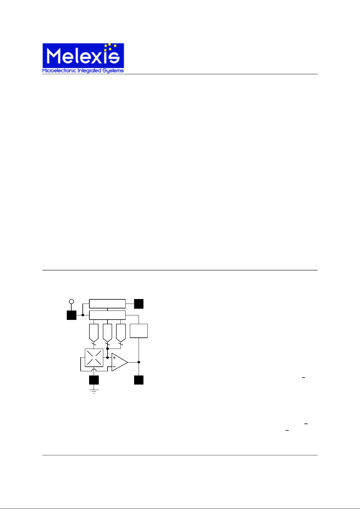
Functional Diagram
Features and Benefits
• Programmable Linear Hall IC
• Quad Switched / Chopper Stabilized
• Ratiometric Output for A/D Interface
• Adjustable Quiescent Voltage (V
OQ
)
• Very Low Quiescent Voltage Temperature Drift
• Adjustable Sensitivity
• Adjustable Temperature Compensation of Sensitivity
Applications
• Linear Position Sensing
• Rotary Position Sensing
• Current Sensing
Ordering Information
Part No. Temperature Suffix Package Temperature Range
MLX90215 L VA(4 Lead SIP) -40°C to 150°C
MLX90215 E VA(4 Lead SIP) -40°C to 85°C
Chopper
Shift Register (RAM)
OTPROM (ROM)
Program
Decoder
1
3
V
DD
2
4
DAC
DAC
DAC
Hall Plate
Pin 1 - VDD (Supply)
Pin 2 - Test/Readback Enable
Pin 3 - VSS (Ground)
Pin 4 - Output
Note: Static sensitive device, please observe ESD precautions.
Page 2

*Patent Pending
MLX90215 Programmable Hall Effect Sensor Rev 4.3 7/6/01 Page 2
MLX90215
Precision Programmable*
Linear Hall Effect Sensor
Parameter Symbol Test Conditions Min Typ Max Units
Supply Voltage VDD Operating 4.5 5.0 5.5 V
Supply Current IDD B = 0, VDD = 5V, I
OUT
= 0 2.5 4.0 6.5 mA
Output Current
(1)
I
OUT
VDD = 5V + 10% -2 - 2 mA
Quiescent Output Voltage
(2)
VOQ 10-Bit Programmable, B = 0 0.5 - 4.5 V
Output Voltage
(1)
VOH V
DD
= 5V, I
OUT
= -2mA 4.50 4.65 V
Bandwidth
(3)
BW RoughGain @ Min - 1.300 kHz
Bandwidth
(3)
BW RoughGain @ Max 0.130 - kHz
Impulse Response Time
(6)
T
RMIN
RoughGain @ Min 25 - µs
Impulse Response Time
(6)
T
RMIN
RoughGain @ Max 250 µs
Offset Voltage Adjustment
Resolution
∆VOQ B = 0, TA = 25oC -1.5 - 1.5 mV
Offset Voltage Drift
over Temperature
∆VOQ/∆T B = 0, TA = -40oC to 150oC
S < 100mV/mT & VOQ > 0.75V
-20 - 20 mV
Offset Voltage Drift
(2)
over Temperature
∆VOQ/∆T B = 0, TA = -40oC to 150oC
S > 100mV/mT & VOQ < 0.75V
-40 - 40 mV
Range of Sensitivity
(7)
s 13-Bit Programmable 5 - 140 mV/mT
Peak to Peak Noise
(4)
8 25 60 mV
Output Resistance R
OUT
6 Ω
Sensitivity Drift
(5)
TA = 25oC -1 - 1 %
MLX90215 Electrical Specifications
Output Voltage
(1)
VOL VDD = 5V, I
OUT
= 2mA 0.35 0.50 V
Sampling Rate f
SAMP
RoughGain @ Max and Min 4 - 40 kHz
Melexis Inc. reserves the right to make changes without further notice to any products herein to improve reliability, function, or design. Melexis does
not assume any liability arising from the use of any product or application of any product or circuit described herein.
Notes:
(1) If output current and voltage specifications are exceeded, linearity will be degraded.
(2) If VOQ is programmed beyond these limits, the temperature compensation may become a problem at high temperatures. It is not recommended to program values of VOQ below 1V or above 4V when sensitivity exceeds 100
mV/mT. Temperature instability can occur on some devices under these conditions.
(3) Bandwidth is inversely proportional to ROUGHGAIN.
(4) Peak to Peak Noise is a function of ROUGHGAIN setting. See page 5, Peak to Peak Noise versus Sensitivity.
(5) Sensitivity drift is indepe ndent of other parameters and does not include individual tolerances (∆V
OQ
or ∆VOQ/∆T).
The tolerance for sensitivity is + 1% of its initial value. This does not include tolerance stack-up.
(6) If the impulse occurs in the middle of a sample interval, the small signal response delay will double. If a 50% to
100% impulse, slew rate may result in double or triple delay.
(7) 1 mT = 10 Gauss
Page 3
*Patent Pending
MLX90215 Programmable Hall Effect Sensor Rev 4.3 7/6/01 Page 3
MLX90215
Precision Programmable*
Linear Hall Effect Sensor
How does it Work?
The MLX90215 programming is done through the
output pin, by changing supply voltage levels. Please
note that the VDD is raised to approximately 13V and
18V during programming. Any connected
components must also tolerate this voltage
excursion. When the supply voltage is at 4.5V to
5.5V, the output behaves normally. If the supply
voltage is raised to 13V, the output then behaves as an
input, or LOAD mode, allowing the 31 -bit word to be
clocked in. All data is loaded through a single line,
with no dedicated clock signal. Clock and data are
integrated into one signal which is initiated with the
beginning of the LOAD sequence, then clocked with
the positive edge of each bit. Variables are changed
with the PC software and loaded into the te mporary
register of the device (RAM) via the timings of the
programmer’s microcontroller. Data can be loaded as
many times as desired while in LOAD mode. Once a
word is loaded, results are checked by observing the
output voltage. This can be done with an external
Voltmeter attached directly to pin 4 of the device, or
with the internal ADC of the programmer. Once the
desired program is loaded, the word can be “Zapped”
permanently into ROM.
This is done when the supply voltage rises above 18V,
or ZAP mode, creating enough current to “Zap” 31
zener diodes which correspond to the temporary
register. The ZAP function is a one-time function and
cannot be erased.
The above description is only for reference. The
voltage levels and data transfer rates are completely
controlled by the ASIC programmer. For more
information on the programmer hardware, contact
Melexis and request a datasheet for the SDAP
programmer.
Programming The Quiescent Offset Voltage (VOQ)
10 bits, 1024 steps of resolution, are allotted to adjust
the Quiescent Offset Voltage (VOQ). By utilizing the
HALFVDD function, the VOQ can be set to one of two
ranges. With the HALFVDD function disabled, the
VOQ can be programmed within a range of 10% to 90%
VDD with about 5mV per step resolution. With the
HALFVDD function enabled, the device may be
programmed within a 2V to 3V window with less than
1mV per step resolution
Programming the Sensitivity (Gain)
The sensitivity is programmed with a ROUGHGAIN
and a FINEGAIN adjustment. The ROUGHGAIN is
adjusted by utilizing three bits, or 8 increments. The
FINEGAIN is programmed with 10 bits or 1024
increments. The sensitivity can be programmed within
a range of 5mV/mT to 140mV/mT. Another 1-bit
function allows the direction of the sensitivity to be
reversed. The INVERTSLOPE function, when
activated, will cause the Voltage output of the
MLX90215 to decrease in the presence of a South
magnetic field, and to increase in the presence of a
North magnetic field. Table 2 expresses examples of
sensitivity resulting from programming ROUGH
GAIN and FINE GAIN codes, with the INVERT
SLOPE function turned off.
Note: Tables 1 and 2 are examples how various codes affect the
UnitsHalfVDD OffsetDAC Output
0
0
0
1
1
1
0
512
1023
0
512
1023
4.97
2.47
0.03
3.07
2.45
1.83
V
V
V
V
V
V
Table 1 - Programming Offset Voltage (VOQ)
RoughGain FineGain Output Units
0
0
1
1
2
2
0
1023
1023
0
4.1
9.4
6.2
14.6
9.5
22.4
mV/mT
Table 2 - Programming Sensitivity
mV/mT
mV/mT
mV/mT
mV/mT
mV/mT
3
3
4
4
5
5
0
1023
1023
0
14.2
33.1
21.5
50.4
31.3
72.5
mV/mT
mV/mT
mV/mT
mV/mT
mV/mT
mV/mT
6
6
46.2
107
mV/mT
mV/mT
7
7
68.9
140
mV/mT
mV/mT
0
1023
0
1023
0
1023
0
1023
Page 4

*Patent Pending
MLX90215 Programmable Hall Effect Sensor Rev 4.3 7/6/01 Page 4
MLX90215
Precision Programmable*
Linear Hall Effect Sensor
Programming the Temperature Compensation
The MLX90215 has a 5-bit (32 step) programmable
adjustment that changes it’s sensitivity drift over a
given temperature range. By adjusting the TC code
the sensitivity can be programmed to increase as
temperature increases to counteract the decrease in
magnetic flux most magnets display over temperature.
For example a SmCo (Samarium Cobalt) magnet has a
temperature coefficient of approximately –300 ppm/
o
C. The MLX90215 can be programmed with a TC of
300 ppm/oC to counteract the TC of the magnet and
greatly improve linearity over temperature.
Table 3 (left) illustrates the way the TC code affects
the sensitivity temperature drift. Also note in Table 3,
the overlap in TC codes. The numbers in the table
represent typical results and are for reference only.
For accurate results the TC code must be determined
experimentally. This Tc code map applies to
MLX90215’s with a second line brand showing
“15DXX”
Special Note
The MLX90215 programmed with a zero TC code
(default) has a typical TC value between the range of –
300 to –600 ppm/oC. This means sensitivity will
decrease slightly as temperature increases. The
slightly negative initial TC value allows the
MLX90215 to be accurately programmed up to 0 TC.
Almost all magnets have a naturally negative TC code.
The natural TC of a magnet added with the initial
negative TC value of the MLX90215 could degrade
linearity over a large temperature span. Using a TC
code of 6, 7, or 8 will give the MLX90215 a slightly
posit ive TC code.
Early revisions of the MLX90215 with second line
brand of “15AXX” should refer to factory for Tc code
TC Code Min Typical Max Units
0 -600 -450 -300 ppm/oC
1 -535 -385 -235 ppm/oC
2 -465 -315 -165 ppm/oC
3 -390 -240 -90 ppm/oC
4 -300 -150 0 ppm/oC
5 -235 -85 65 ppm/oC
6 -150 0 150 ppm/oC
7 -85 65 215 ppm/oC
8 125 275 425 ppm/oC
9 125 360 510 ppm/oC
10 210 435 585 ppm/oC
11 285 515 665 ppm/oC
12 450 600 750 ppm/oC
13 535 685 835 ppm/oC
14 600 750 900 ppm/oC
15 680 830 980 ppm/oC
16 1150 1300 1450 ppm/oC
17 1230 1380 1530 ppm/oC
18 1320 1470 1620 ppm/oC
19 1405 1555 1705 ppm/oC
20 1490 1640 1790 ppm/oC
21 1575 1725 1875 ppm/oC
22 1665 1815 1965 ppm/oC
23 1750 1900 2950 ppm/oC
24 2165 2365 2565 ppm/oC
25 2340 2490 2640 ppm/oC
26 2425 2575 2725 ppm/oC
27 2500 2650 2800 ppm/oC
28 2595 2745 2895 ppm/oC
29 2680 2830 2980 ppm/oC
30 2710 2910 3110 ppm/oC
31 2775 2975 3175 ppm/oC
Table 3 - Temperature Compensation
Condition Output Level
V
OUT
Shorted to VDD V
OUT
= VDD
V
OUT
Shorted to VSS V
OUT
= VSS
V
OUT
open with pull up load V
OUT
= VDD
V
OUT
open with pull down load V
OUT
= VSS
VSS open with pull up load V
OUT
= VDD
VSS open with pull down load
> 10 K Ohms
V
OUT
= VDD
or 94% VDD
VDD open with pull up load
> 4.7 K Ohms
V
OUT
= VSS
or 3% VDD
VDD open with pull down load V
OUT
= VSS
Temperature Compensation
Temperature compensation (TC) is defined as the
change in sensitivity over temperature. Expressed in
(Parts Per Million per Degree Celcius) ppm/oC.
SensT1 = Sensitivity measured at Temperature 1 (T1)
SensT2 = Sensitivity measured at Temperature 2 (T2)
Sens25 = Initial Sensitivity measured at 25oC
C
ppm
TTSens
SensSens
TC
o
TT
6
25
21
10
21
1
∗
−
∗
−
=
Page 5

*Patent Pending
MLX90215 Programmable Hall Effect Sensor Rev 4.3 7/6/01 Page 5
MLX90215
Precision Programmable*
Linear Hall Effect Sensor
5
4
3
2
1
0
0
-6
-12
-18
6
12
18
Output Voltage (V)
Flux Density (mT)
Typical Output Voltage versus
Magnetic Flux Density
Sensitivity = 140mV/mT
MLX90215
5
4
3
2
1
0
0
-90
-180
-270
90
180
270
Output Voltage (V)
Flux Density (mT)
Typical Output Voltage versus
Magnetic Flux Density
Sensitivity = 10mV/mT
MLX90215
32.7
25.4
18.1
10.8
3.5
3210 4 5 6
Sample Rate (kHz)
RoughGain (PA) Value
Typical Sample Rate
versus
Rough Gain (PA)
MLX90215
7
40
50
40
30
20
10
0
65
40
15
5
90
115
140
Output Voltage (mV)
Sensitivity (mV/mT)
Typical Peak to Peak Noise
versus
Sensitivity
60
MLX90215
MLX90215 Performance
Page 6

*Patent Pending
MLX90215 Programmable Hall Effect Sensor Rev 4.3 7/6/01 Page 6
MLX90215
Precision Programmable*
Linear Hall Effect Sensor
.
Supply Voltage (Over Voltage) 18V
Supply Voltage (Operating) 5V + 10%
Reverse Voltage Protection -14.5V
Magnetic Flux Density Unlimited
Supply Current, IDD 6.5 mA
Output Current (Short to VDD) +12 mA
Output Current (Short to VSS) -12 mA
Operating Temperature Range, TA -40°C to 150°C
Storage Temperature Range, TS -55°C to 165°C
ESD Sensitivity +7kV
Absolute Maximum Ratings
Pin Description
Recommended Wiring
MLX
90215
V
DD
1 2 3 4
C1 C2
Pin1 V
DD
Pin2 Test*
Pin3 V
SS
Pin4 OUT
C1 = 2.5nF
C2 = 2.5nF
Mutilayer surface mount
capacitors recommended
*Readback diagnostic use only. Pin 2 is NOT for
programming device. For best results, tie to GND.
Melexis Programmer
Melexis offers a programmer (PTC-01) for progra mming the MLX90215. The PTC-01 comes complete
with windows based software that makes programming
the MLX90215 simple. The programmer communicates with a PC via a RS232 serial interface. The programmer and software allows users to load settings in
the MLX90215, take measurements, calibrate sensors,
and program the MLX90215. For more information
the PTC-01 goto
www.melexis.com, or contact Melexis.
Left, PTC -01 windows
based software.
Works with any IBM
compatible PC running windows 9x.
Melexis PTC-01
Programmer
Page 7

*Patent Pending
MLX90215 Programmable Hall Effect Sensor Rev 4.3 7/6/01 Page 7
MLX90215
Precision Programmable*
Linear Hall Effect Sensor
Clamping the Output Voltage
The MLX90215 has a 2-bit CLAMP feature which
allows Four output voltage options. The CLAMP fe ature is independent of the gain, and will not effect se nsitivity of the device. The table below illustrates limits
for each of the four options.
Bit Value Limits (% VDD)
0 (default)) no clamp
1 5 to 45
2 10 to 90
3 5 to 95
Application Comments
The following is a list of recommended operating parameters that will help to ensure the accuracy and stability of the MLX90215. These are not the absolute
programming limits of the device.
1.) Voq is best programmed in the absence of any
magnetic influence and to voltages closest to 1/2
VDD, where temperature drift will be +/-0.4% or
less. It is not recommended to use VOQ values close
to 0 volts or VDD when programming extremely
high sensitivity (> 100 mV/mT) values. Tempera ture instability may be observed on some devices
under these conditions.
2.) Best linearity of sensitivity is obtained when VOQ
is programmed at 1/2 VDD. This is with the 1/2
VDD function enabled.
3.) Best linearity of sensitivity is obtained when the
gain is programmed between 5mV/mT and
100mV/mT.
4.) Best temperature stability is realized when the
temperature compensation function is programmed
to zero ppm/oC.
5.) The Test/Readback pin is for diagnostic use only.
This pin is normally tied to GND. Contact Melexis
for more details on programming this device.
Installation Comments
1.) Avoid mechanical stress on leads or package.
Stress may cause VOQ shift.
A.) Avoid bending leads at the package interface.
B.) Support the leads by clamping, when bend
ing.
C.) Avoid gluing device to another material. This
may cause temperature-related stress.
2.) CMOS products are static sensitive devices, please
observe ESD precautions.
3.) Observe temperature limits during soldering.
Bit Allocation Table
Bit Function
1 INVERTSLOPE
2 OFFSETDAC 5
3 OFFSETDAC 6
4 OFFSETDAC 7
5 OFFSETDAC 8
6 OFFSETDAC 9
7 OFFSETDAC 4
8 OFFSETDAC 3
9 OFFSETDAC 2
10 OFFSETDAC 1
11 OFFSETDAC 0
12 FINEGAIN 0
13 FINEGAIN 1
14 FINEGAIN 2
15 HALFVDD
16 FINEGAIN 3
17 FINEGAIN 4
18 FINEGAIN 5
19 FINEGAIN 8
20 FINEGAIN 9
22 FINEGAIN 7
23 ROUGHGAIN 2
24 ROUGHGAIN 1
25 ROUGHGAIN 0
26 TEMP CO 0
27 TEMP CO 1
28 TEMP CO 2
29 TEMP CO 3
30 TEMP CO 4
31 CLAMP 1
32 CLAMP 0
33 MEMLOCK
34 TEST 0
35 TEST 1
36 TEST 2
37 TEST 3
21 FINEGAIN 6
Page 8

*Patent Pending
MLX90215 Programmable Hall Effect Sensor Rev 4.3 7/6/01 Page 8
MLX90215
Precision Programmable*
Linear Hall Effect Sensor
Physical Characteristics
All Dimensions in millimeters
VA Hall Plate / Chip Location
VA Package Dimensions
Notes:
1. Pinout: Pin 1 V
DD
Pin 2 Test/Readback
Pin 3 GND
Pin 4 Output
2. Controlling dimension: mm .
3. Leads must be free of flash and plating voids.
4. Leads must not arc toward the rear of package.
5. VA lead frame material: C151.
6. VA molding compound: Sumitomo EME 6300H.
7. Package dimensions exclude molding flash.
8. Tolerance: +/- 0.254 mm unless otherwise specified.
9
. *Marking:
Line 1:
1st and 2nd digits (00) = Year (2000)
3rd and 4th digits (14) = Week of Year
Line 2:
1st and 2nd digits (15) = Chip I.D. (90215)
3rd digit (D) = Chip Revision
4th and 5th digits(88) = Lot Number
2.86
1.86
2.18
Hall Plate
0.20 x
0.20
2.69
0.387
0.289
Marked
Surface
E
3.46
3.30
A
B
C
5
o
(2x)
5
o
(2x)
0.387
0.289
3.79
3.63
D
F
G
H
1.0
MA
X
0.22
REF
0.45
0.35
4.50
4.10
45o X 1mm
15.50
14.50
0014
15D88
*
1 2 3
4
5.08
5.24
5.33
5.43
1.22
1.32 3.76
3.86
J
VA
1.20
1.10
0.66
0.61
0.29
0.24
45
o
0.31
0.18
B
A
C
D
E
0.15
0.0
F
G
H
0.60
0.40
0.35
0.25
J
45
o
For the latest version of this document,
Go to our Website at:
WWW.Melexis.Com
For additional information
Contact Melexis direct at:
Europe and Japan USA and Rest of World
E-mail: sales_europe@melexis.com Sales_usa@melexis.com
Phone: 011-32-13-670-780 (603) 223-2362
Page 9

*Patent Pending
MLX90215 Programmable Hall Effect Sensor Rev 4.3 7/6/01 Page 9
MLX90215
Precision Programmable*
Linear Hall Effect Sensor
Application Notes
5
4
3
2
1
0
0-100 100
Current (Amps)
V
OUT
(Volts)
MLX
90215
V
DD
A slotted ferrite
toroidal core and a
series of windings are
the main elements of a
current sensor. By
adding a
programmable Hall IC
to the air gap, not only
can the output be
calibrated accurately,
but it can also be
adjusted to respond to
virtually any range of
current
Programmable Current Sensor
Linear Precision Current Sensor
The Programmable gain, offset, and temperature co mpensation of MLX90215 allows great flexiblity in the
design of a current sensor.
Current flowing through a conductor can produce a
proportional magnet field. The MLX90215 can then
produce an output voltage proportional to the current.
Using the programmable gain and offset function the
output of the MLX90215 can be adjusted to sense a
wide range of current allowing for a flexible design.
Slotted Torroid Example Assuming infinite permeabilty of the core, the magnetic field through the air
gap produced by a single wire turn is given by equ ation 2
Equation 2
Where: I = current in Amperes
B = magnetic field in Tesla
lg = length of air gap in Meters
uo = Permeabili ty of free space (4π10-7H/m)
This equation is a close estimate for the field in the air
gap, but does not take into account magnetic losses in
the core, fringing effects, and mechanical tolerances of
the air gap. The programmable MLX90215 can be
adjusted to compensate for these errors simplifying the
design. The temperature compensation of MLX90215
can also be adjusted to counteract temperature losses
of core.
For sensing a current ±100A, with an air gap of 2mm
equation 2 yields a magnetic field range of ±63mT.
The output range of the MLX90215 is 0.5V to 4.5V
(4V full scale). Equations 3a and 3b yield a sensitivity
of 32mV/mT and a Voq of 2.5V.
Equation 3
a) S = 4000mV/ 126mT
b) Voq = 4V/2 + 0.5V
The resulting gain of the current sensor is 20mV/A
with an offset of 2.5V. For best results it is recommend
that MLX90215 be programmed with a Voq of 50%
Vdd 1/2 Vdd bit set.
o
g
u
l
I
B =
Magnetic Suppliers
Elna Ferrites Technologies Inc
Eastern Components
Fair Rite Products Corp
 Loading...