

Page 1

MLX90111
128bit Read Write Transponder
Features
- 144bit EEPROM code, flexible Read Write Transponder IC
- Very Big reading range, and large write range.
- ID configured as 8 user words of 16 bits, and multiple write protection levels, including OTP
- 16 bit Configuration word with lock flags per word and option bits
- Different encoding and datarate options
- 250pF integrated tuning capacitance with wide post assembly tuning range
- 100,000 write cycle, 10 year EEPROM retention
- Guaranteed data integrity for reliable programming
Applications
Animal ID (ISO 11784, -85 compliant), ATM, Access Control, Material Logistics, Overmoulded
assemblies with important detuning effects.
Ordering Information
Part No. Temperature Range Package
MLX90111 25 °C Consumer Sawed wafer on frame
-40 to 85 °C Automotive Bare die in blistertape
SOIC-8 150mils
Production parts available Q1 2001
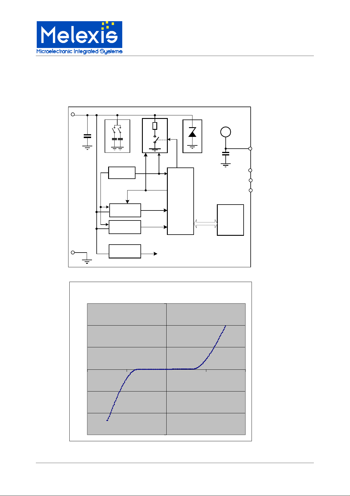
Functional Diagram Description
The MLX90111 is a flexible 128 bit Read Write
Transponder IC operating at 125kHz. It has been
designed for high performant and highly reliable RFID
systems requiring multiple write access to the
transponder memory.
MLX90111
Coil
L
GND
C
tune
Clock and power supply are taken from the
electromagnetic field. A resistor is switched in parallel to
the resonant circuit formed by the integrated tuning
capacitor and the external coil, to amplitude modulate
the electromagnetic field. Encoding of the 128 bits ID
and data rate can be defined by setting the
corresponding EEPROM bits.
High quality factors can be applied as the frequency can
be tuned over a range of +/-10% to +/-0.5% accurate
after assembly, by changing the value of the tuning
capacitor up to +/- 2pF.
The EEPROM is configured as 11 words of 16 bits.
Words 1 to 8 form the ID and are continuously read out
during normal operation. Each of these can be
individually locked, or the complete EEPROM can be set
to read only.
The transponder can be written over the full range from
0% to 60% of the normal reading distance. The
transponder stops modulating when receiving an AM
asynchronous pattern. It will then synchronize on the
first bit it receives. The 32 bit write command is
transmitted using Return to One modulation, including
direct word addressing and multiple security checks.
Data integrity is guaranteed by critical read out after
programming.
MLX90111 128bit Read Write Transponder Page 1 of 12 Rev 1.12 5-Feb-01
Page 2

MLX90111
128bit Read Write Transponder
MLX90111 Electrical Specifications
Operating Parameters are based on test set up (see Schematic below).
Toper = -40°C to 85°C, Operating frequency = 120kHz (unless otherwise specified)
Parameter Symbol Test Conditions Min Typ Max Units
Regulated supply voltage VDD (3) 3.0 4.0 V
Power On Level VPOR Continuous normal reading of the ID 1.55 1.8 2.2 V
Sensitivity level (e.m.f.) Vacsens Continuous normal reading of the ID 200 170 mV
Modulation Depth ASK
Weak power: Vacmin = 200mVpp 0.2 4 V(4)
Medium power: Vac = 5Vpp 2.8 7.5 V(4)
High power: Vac = 20Vpp 5 10 V(4)
EEPROM writing supply voltage Vacee Critical reading ID 1 V
EEPROM writing supply current Iee 10
ACP modulation depth Vachigh=Vacee 20
µA
% (5)
EEPROM data retention Tret Critical reading ID 10 year
EEPROM write cycles Ncycle Critical reading ID 100k cycles
Coil-GND tune capacitor Toper=25oC 200 pF(6)
Total Tuning range Toper=25oC, 5bits 124 pF(6)
Tuning accuracy Toper=25oC, LSB/2 2.0 pF(6)
IclampLow VdutDC = +/- 2V 40 1000 NADC input current clamping
IclampHigh VdutDC = +/- 10V 1 3.5 10 mA
Notes:
Note (1): Specifications are tested 100% or
guaranteed by characterization.
Vin
L=6.8mH
Cpar=10pF
Vdut
COIL
Note (2): All specifications are valid for Manchester
and Biphase encoding, and for 2kbaud and 4kbaud
data rate options.
50
Qrc @ 120KHz=48.8
C1+C2=250pF
Vac
C1 C2
GND
90111
DUT
Note (3): Maximum supply voltage is generated by
forcing 10mA between coil and ground pin.
Note (4): Min = Vbottom (modulation on),
Max = Vtop (modulation off).
Note (5): Modulation depth is calculated as Vachigh -Vaclow / Vachigh + Vaclow. Lower modulation depths may
be applied, but the performance of the system may vary along the distance between reader and transponder coil.
Higher modulation levels will reduce the maximum Write distance.
Note (6): Lot to lot spread on capacitance is 20%. Temperature shift is typically 0% on -40°C, and +1% at 85°C.
MLX90111 128bit Read Write Transponder Page 2 of 12 Rev 1.12 5-Feb-01
Page 3
Block diagram
COIL
MLX90111
128bit Read Write Transponder
VSS
Ctune
[mA]
15
Trimming
POR
CLOCK
RECOVERY
DEMODUL.
SUPPLY
Modulator
SPEED
CLOCK
DATA
VDD
M
O
D
Digital
Controller
RF Limiter
Cbuffer
ADDR
DATA
MLX90111 clamping (DC)
VDD
VDD
TCKIN
TEST
DATAIO
EEPROM
10
5
0
[V]
-20 -10 0 10 20
-5
-10
-15
MLX90111 128bit Read Write Transponder Page 3 of 12 Rev 1.12 5-Feb-01
Page 4
EEPROM memory maps
ADDRESS
FUNCTION
COMMAND
F E D C B A 9 8 7 6 5 4 3 2 1 0
0
1
2
3
ID
4
5
6
7
Read memory map
CONTINUOUS
MLX90111
128bit Read Write Transponder
BITPOSITION (MSB first)
B
WPW
C
Tune+CFG
ADDRESS
FUNCTION
0
1
2
3
ID
4
5
6
7
Lock word: "01010101" WPW(FLAGS)
CMF1
0
CMF1
COMMAND
CMF1
T4T3T2T1T0
F E D C B A 9 8 7 6 5 4 3 2 1 0
Write memory map
8
WPW
Lock word: "01010101" WPW(FLAGS)
CMF2
0
0
0
0
0
BITPOSITION (MSB first)
0
0
0
CODE
SPEED
9
Tune
A
CFG
MLX90111 128bit Read Write Transponder Page 4 of 12 Rev 1.12 5-Feb-01
CMF2
CMF2
0
T4T3T2T1T0
0
0
0
0
0
0
0
0
0
0
0
0
0
0
0
0
0
0
0
0
0
0
0
0
CODE
SPEED
Page 5

MLX90111
128bit Read Write Transponder
General Description
The MLX90111 is a 128bit Read Write
transponder IC. The integrated tune
capacitance and the external coil form a
resonant LC antenna that absorbs part of the
electromagnetic energy radiated by the
transceiver LC antenna. Physically, a magnetic
coupling occurs between the transceiver, also
referred to as "reader", and transponder
antennas
To amplitude modulate (AM) the RF carrier, the
transponder damps the electromagnetic field by
switching a resistor in parallel with its coil. This
way the transponder repetitively transmits its
128bit-identification code (ID) to the transceiver,
which recovers the envelope of the damped
field, and decodes the ID.
The transceiver can send commands and data
to the transponder by modulating the amplitude
of the carrier.
POR level
When the transponder is placed in an external
radio frequency (RF) field of appropriate
frequency and amplitude, the internal power
supply (VDD) can build up as charge on the
integrated buffer capacitance. The modulation
resistor is switched on and off as soon as VDD
has reached the Power On Reset (POR) level.
When the modulation resistor is switched on, the
LC circuit is no longer tuned, therefore no
energy is taken from the field, and VDD drops
due to internal consumption. Hence, by
switching the modulation resistor on and off, it is
possible to oscillate around the POR level. This
phenomenon is referred to as hiccuping.
The modulation resistor is switched off when the
transponder drops below the POR level.
Sensitivity level
The minimum electromagnetic force (e.m.f.)
needed to avoid hiccuping is defined by
Vacsens. At this level the power supply will not
drop below the POR level while the modulation
resistance is switched on during modulation.
Demodulator
If the external RF field is AM modulated
according to the asynchronous control pattern
(ACP), the transponder stops transmitting the ID
and enters the Program Mode.
Data is then sent to the transponder using
Return to One encoding. First half bit is low (0)
or high (1), and the second half is high. In the
middle of each half bit one sample is taken. In
order for the transponder to detect the ACP
modulation a minimum modulation depth is
required. See timing specification below for
more details on the write protocol.
RF limiter, or clamping
The build up of voltage on the resonant LC
circuit is limited to avoid damaging the internal
circuit.
Modulator
The modulator consists of a modulation resistor
that is switched in parallel with the resonant LC
circuit (antenna). Because in weak RF fields the
rising edge is much slower than the falling edge
of the envelope, a symmetrically driven
modulator would give an asymmetrical envelope.
This is anticipated by delaying each falling edge
by a fixed number of RF clock pulses. The
modulator is hence driven asymmetrical. Each
ON state is reduced by 8 (4) clocks in 2 (4)
kBaud mode, and each OFF state is prolonged
by the same amount.
Speed Total clocks
per Bit
2kbaud 64 Long ON = 64 - 8
4kbaud 32 Long ON = 32 – 4
Clocks ‘ON’ state Clocks ‘OFF’ state
Long ON = 64 + 8
Short ON = 32 - 8
Short ON = 16 – 4
Short ON = 32 + 8
Long ON = 32 + 4
Short ON = 16 + 4
Clock recovery
The transponder takes its clock from the carrier
frequency. Depending on the speed option, the
carrier frequency is divided by 32(4kbaud),
64(2kbaud) to generate the bit rate.
MLX90111 128bit Read Write Transponder Page 5 of 12 Rev 1.12 5-Feb-01
Page 6

EEPROM
1. Memory organization
The EEPROM memory is arranged as 11 words
of 16 bits each (see memory map above). Each
one of these words is individually programmable.
1.1 ID (Addresses #0 to #7)
The first 8 words hold the 128bits identification
code (ID). Any of the 8 words of the ID can be
individually written. The complete 128bits ID is
send out when the device is in continuous/critical
read mode.
1.2 Write Protect Word (Address #8)
The 9th word allows writing protect some words
from the ID temporarily or permanently, or even
block the complete ID: OTP feature.
Bits 0 to 7 (WPW flags) lock (1) or unlock (0)
the write access to the corresponding word in
the ID.
The most significant byte (Lock WPW) is
ignored, except when written with a special
pattern (01010101 -MSB to LSB-). Then it locks
the WPW (#8), the Tuning bits (#9) and the
Configuration word (#10). When writing
FF55Hex to the WPW word, then the
transponder becomes an OTP device.
1.3 Tuning bits (Address #9)
The tune bits select the status of the tuning
capacitors (1=on, 0=off).
They can be written with command CMF2 at
address 9 in the bit positions 14 to 10 (from the
highest, 64 pF to the lowest, 4 pF). The tune bits
can be read back at address 12 with command
CMF1. As the tune bits do not overlap with the
configuration bits they can be read together in
word 12. Programming is kept separate, to
avoid reprogramming of the tune bits in case the
code/speed is changed.
The Tune capacitance can be delivered tuned to
an absolute value of 250pF +/-2%, leaving 5%
tuning after assembly, or tuned for maximum
tuning range after assembly. The latter solution
can only be provided with an absolute value
ranging between 200 and 300pF, but over full lot
tuned to 2%. This offer is only valid for large
volume orders (>100k pieces).
MLX90111
128bit Read Write Transponder
Following table shows the configuration of the
tune caps in relation to the tune bits:
Tune bit Nominal capacitor
value (pf)
T4 64
T3 32
T2 16
T1 8
T0 4
1.4 Configuration Word (Address #10)
Speed bit (bit 0) defines the internal clock
extraction: set to 1 for divided by 32, set to 0 for
divided by 64.
SPEED Data rate Baud rate
0 Freq/64 2kbaud
1 Freq/32 4kbaud
Code bit (bit 1) defines if the ID will be encoded
in Manchester (set to 1) or Biphase (set to 0)
amplitude modulation scheme.
CODE Encoding
0 Biphase
1 Manchester
MLX90111 128bit Read Write Transponder Page 6 of 12 Rev 1.12 5-Feb-01
Page 7

MLX90111
128bit Read Write Transponder
2. Operating Modes
2.1 Continuous/critical read mode (ID)
In read mode, the transponder transmits its ID
code to a transceiver by amplitude modulating
(AM) the envelope of the carrier coming from the
transceiver. The 128 bits of the ID are
Manchester or Biphase encoded.
After POR the device will enter 'normal' read
mode. The ID will be read out under optimal
conditions. After programming any word of the
ID, the device will automatically enter 'critical'
read mode. The data is read at the 2 extremes
of the reading window. When both readings are
identical, the data retention is guaranteed as
specified (Tret, Ncyc). If the two critical readings
show a difference, the device is at its minimum
coupling with the transceiver and it should be
reprogrammed using a stronger field.
Critical read mode can only be reset by
removing the transponder from the RF field.
2.2 Programming mode
Upon receiving an Asynchronous Control
Pattern (ACP), the device enters program mode
and waits during a Watchdog Delay period
(TWD), for the start bit of the programming
sequence.
The programming sequence consists of a start
bit, and a 32 bit command. The command starts
with a 3bit Command Field (CMF), a 4bit
address, an odd parity bit calculated over the
address, a 16bit data word and an 8bit CRC
calculated over the full command.
If the programming sequence is received, the
write access, parity and CRC are verified and
command is executed if possible, else the
transponders goes back into normal read mode.
In case the command has been executed, the
transponder waits again for a Watchdog Delay
period TWD for a new programming command.
In case of a timeout the device starts sending
the ID code in critical read mode, until removal
from the RF field.
Minimum field strength for reliable programming is
set by the minimum induced e.m.f. Vacee on the
transponder coil.
2.3 Programming commands
Two Command Fields are defined:
CMF Code Action
CMF1 001 - Write ID words: addresses 0…7,
- Read address 8,9,10
CMF2 000 - Write address 8,9,10
To write data, the respective CMF and address
are sent out. If the write access, parity and CRC
are verified, the data are written in the EEPROM
at the specified location. For 2kbaud devices
EEPROM programming takes 20ms, for 4kbaud
devices programming is done in 10ms.
To read the data in addresses 8, 9 and 10 CMF1
is used.
- address 11 for reading the configuration word.
- address 12 for reading the tuning (bit positions
14 to 10) and the configuration (bit positions 0 to
1) bits, see the memory map.
If the parity and CRC are verified, the data is
sent out during the time window normally
allocated for the EEPROM programming. Data
is sent with a start bit of ½ bit (!) time first,
followed by twice the 16-bit data word, with
critical read levels. The startbit allows to detect
a leading 0 in Manchester coding, and allows the
microcontroller to synchronize. Remark that this
startbit is different from the start bit sent by the
reader, which is a full bit.
HINT: In case the reader requires more time to
switch from write to read mode, the dummy data
should be chosen such that the last CRC bits
are 1, i.e. in Return to Zero code: no modulation
needed on the reader antenna. This way the
time for switching the reader can be extended.
2.3 Parity, CRC
PAR is an odd Parity bit is calculated over the 4bit address
The 8-bit CRC with polynomial u8+ u4+ u3+ u2+
u0 is calculated over the complete command
string [CMF-ADDRESS-PAR-DATA].
2
u
3
u
4
u
8
u
LSB
Exclusive OR
Register Stage
x
35 467 2 01
MSB
Data
MLX90111 128bit Read Write Transponder Page 7 of 12 Rev 1.12 5-Feb-01
Page 8

3 Timing specification
3.1 Asynchronous Control Pattern
The Asynchronous Control Pattern (ACP) is sent
by the reader to render the transponder silent
(stop transmitting), and listen for a programming
sequence.
Before starting the ACP, the field must be stable
at FHIGH for at least 5 bit periods (Tsetup). This
guarantees that the reference level
FTHRESHOLD is adjusted.
The control pattern itself contains 4 transitions
between high field FHIGH and low field FLOW,
each of which should be 2.5bitperiods apart.
The threshold level FTHRESHOLD adjusts itself
exponentially to the average FHIGH over the last
20 periods (TCLK).
The optimum modulation depth forced by the
reader depends on the application and stretches
between:
90%> (FHIGH-FLOW) / (FHIGH+FLOW) > 20%
The transponder samples the field 2 times per
bit. A first time is after the first quarter, the
second time after the third quarter. The sample
values are only retained when the modulation
resistor is off. The other samples are dropped.
3.2 Synchronous Command
When the ACP has been detected, the
transponder modulation will be turned off, within
maximum 6 bit periods after the last rising edge
of the ACP. The transponder will now
synchronize on the first falling edge it sees. This
edge is generated by a startbit (SB=0), which
has to be sent within a Timeout Window TWD.
If no SB is detected the transponder will return to
its original read mode.
The SB may used to optimize the
synchronization between tag and reader.
Tip: always try to put the sampling time of the
transponder at the end of the first half bit. This
minimizes the influence of an increased the
transponder Q at larger distance.
However, if the modulated signal on the
transponder takes several periods to drop, the
SB may be extended with this time. This will
shift the sampling moment forward.
After this synchronisation step, a synchronous
command can be sent from the base station.
Make sure to respect the nr of transponder
clocks per bit, as specified below.
All data sent by the reader have to be ReturnTo-One encoded.
MLX90111
128bit Read Write Transponder
3.3 Transponder action
The command is verified on its Parity and CRC
values after the full command has been
received.
If verification is successful the command will be
executed during the next 32 bit periods.
Else if no valid command is received, due to a
verification error, the transponder will
immediately, i.e. 32 bit periods after the SB, start
modulating its 128bit ID code.
3.3 Multiple commands
After successfully receiving a command, the
transponder will wait for a new command. This
new timeout window (TWD) starts after the 32 bit
period it requires to execute the received
command.
To limit time skew between microcontroller and
the transponder, a new synchronization is done
before each new command.
The transponder will start modulating its ID code
approximately 52 btiperiods after successfully
having received its last command.
3.4 Other timings
See timing table below for an overview of all
timings. All timings are bitperiod based, and are
therefore related to the resonance frequency
and datarate.
MLX90111 128bit Read Write Transponder Page 8 of 12 Rev 1.12 5-Feb-01
Page 9

MLX90111
128bit Read Write Transponder
Data send to transponder as number of bit periods
Asynchron Tsetup ACP TWD TWD
Synchron SB CMF ADDR PAR DATA CRC PROG/READ SB
Bit periods >5 3*Tas
+ 6bit
Transponder mode / operations
Normal read Enter program mode:
- Stop modulation
- Synchronize on Start bit
MLX90111 Timing Specifications in ms for a Carrier Freq = 125kHz, Tclk=8µµs
Speed Bit Period Tas TWD PROG/READ
20 1 3 4 1 16 8 32 20 1
Read (32-bit) command Verify command
+ Write / Read
Resynchronize
on Start bit
EEPROM data
Min (2 bit) Max (3 bit) 20 bit 32 bit
Tclk*128 Tclk*192 Tclk*1280 Tclk*2048
Freq/64 (2kbaud) Tclk*64 = 0.512 1.024 1.536 10.24 16.384
Freq/32 (4kbaud) Tclk*32 = 0.256 0.55 0.7 5.12 8.192
1. Modulation on Reader Antenna
Tsetup ACP pattern
FHIGH
FLOW
Tas
Tas
Tas
6bit
2. Modulation on Tag Antenna
FHIGH
FTHRESHOLD
FLOW
Biphase: 1 1 1 0 0 1 1 1 0 1 1 - - - -
Twd
0 - 0 0 1- ...
SB-CMF1- ...
3. 1+2 Superposed on Tag Antenna
- X: samples taken by transponder
- Dark shaded: reader coil modulation ON
- Light shaded: reader coil modulation OFF
MLX90111 128bit Read Write Transponder Page 9 of 12 Rev 1.12 5-Feb-01
Page 10

Manchester Code
MLX90111
128bit Read Write Transponder
Binary Data
Memory Output
Modulation Output
Biphase Code
Binary Data
Memory Output
Modulation Output
Return to One
Binary Data
Binary form
Modulation Output
X
X
X
1
1 1 1 0 1 0
0
1 1 0 1 0 0
1
1 1 1 0 1 0
1 1 0 0
1 1 0 0
1 1 0 0
Coding schemes
Manchester
For a “1” bit, there is a transition from 0 to 1 in
the middle of the bit period. Reciprocal, for a “0”
logic bit there is a transition from 1 to 0 in the
middle of the bit period.
Biphase
At the beginning of each bit, a transition will
occur. A logic bit “1” will keep its state for the
whole bit duration and a logic bit “0” will show a
transition in the middle of the bit duration.
Return to One
This encoding is used to modulate the reader
antenna to send the commands to the
transponder.
For a “0” bit, there is a transition to 0 in the
beginning of the bit period. In the middle of the
bit period the state returns to 1.
For a “1” bit, the level remains high for the entire
bit period.
Flow Chart.
Upon entering the RF field, the transponder
"sees" increasing amplitude of the voltage
between COIL and GND pins. It passes through
a POR sequence, and enters the normal read
mode, transmitting the ID continuously.
If the reader sends an asynchronous control
pattern (ACP), the transponder enters program
mode. It receives an address, parity, a 16-bit
data word and a CRC.
When a write command has been successfully
received, the word is stored at the given
address. When a word of the ID is written, the
critical read flag will be set. This flag can only
be reset by removing the transponder from the
electromagnetic field.
When a read command for addresses #B
(WPW) or #C (tune-bits, speed and code) has
successfully been received, the transponder
immediately sends back the requested
information, once critical high and once critical
low.
If no new programming pattern is received
during the Watchdog Delay period (TWD), the
transponder checks the critical read flag and
enters the appropriate read mode.
MLX90111 128bit Read Write Transponder Page 10 of 12 Rev 1.12 5-Feb-01
Page 11

Flow Chart.
MLX90111
128bit Read Write Transponder
POR
No
Continuous
Normal
Read
(Transmit ID)
ASYNC
detected
Y
Stop modulating
Y
Watchdog expired?
Critical Read=1?
Yes
Continuous
Critical
Read
(Transmit ID)
Addresses:
0..7: Write Id
8: Write WPW
9: Write Tune bits
A: Write Code, Speed bits
B: Read WPW
C: Read Tune, code and Speed bits
N
N
N
Parity/WPW/CRC check
OK?
Y
Write to ID?
address[0..7]
N
Write to
address 8/9/A?
N
Read
address B or C?
Y
Y
Y
Set Critical Read=1
Program word in EEPROM
Read Critical
(Once High, Once Low)
MLX90111 128bit Read Write Transponder Page 11 of 12 Rev 1.12 5-Feb-01
Page 12

MLX90111
128bit Read Write Transponder
Unique Features
• Flexible configuration.
• Simple fast programming.
• Large programming range.
• State of the art reading distance.
• 20% tuning range of resonance frequency
after assembly.
Cross Reference
This product can typically replace Marin
EM4069, TEMIC e5550, Philips HITAG or any
other RW transponder in the 120kHz range.
It provides an easy configurable, high
performant replacement.
Absolute Maximum Ratings
Maximum Power Supply (VDDmax) -0.7 to 7V
Maximum current forced between coil and
ground pin (Icoilmax)
Operating Frequency (Freq) 60 to 150kHz
Normal Operating Temperature (Toper)
Maximum Storage Temperature in SO8
(Tstore)
Electrostatic discharge (HBM) on coil pin
(Vesdcoil)
Electrostatic discharge (HBM) on other pins
(Vesd)
+ / - 30mA
-40 to 85°C
-55 to 125°C
500V
1500V
SO8 Pinout
Pin Name Function
1 COIL Coil connection 1
2 TEST Pin to set chip in test mode
3 TEST Pin to set chip in test mode
Keeping at Vdd/2 will reset the chip
4 VSS(*) Coil connection 2 / ground connection
5 VSS(*) Coil connection 2 / ground connection
6 TEST Pin to set chip in test mode
7 VDD External chip supply for test mode
8 VSS (*) Coil connection 2 / ground connection
(*) All three VSS pins are connected together
thanks to the use of a fused lead frame.
COIL
TEST
TEST
VSS
1
2
3
4
MLX
90111
8
VSS
7
VDD
6
TEST
5
VSS
Chip dimensions
These are good approximations; exact position
info is available on request.
ESD Precautions
2130
Electronic semiconductor products are sensitive
to Electro Static Discharge (ESD).
Always observe Electro Static Discharge control
procedures whenever handling semiconductor
products.
Disclaimer
Melexis reserves the right to periodically make
modifications to product specifications. The
information included herein is believed to be
1630
600
4
1
600
67
accurate and reliable. However, Melexis
assumes no responsibility for its use, nor for any
2 3
infringements of patents or other rights of third
parties which may result from its use.
MLX90111 128bit Read Write Transponder Page 12 of 12 Rev 1.12 5-Feb-01
 Loading...