

Page 1

Micro Linear
March 1997
ML6622*
High-Speed Data Quantizer
GENERAL DESCRIPTION
The ML6622 high-speed data quantizer (post-amplifier) is
a low noise, wide-band, BiCMOS monolithic IC designed
for high-speed signal recovery applications, such as FDDI,
Fast Ethernet, and ATM. An internal DC restoration
feedback loop nulls any offset voltage produced in the
input stage. The limiting amplifier contributes to a high
level of sensitivity and a minimum of duty cycle
distortion.
FEATURES
■ 200 MHz bandwidth
■ Low noise design
■ Adjustable Link Detect function
■ Low power design: 35mA typical
■ Used with the ML6633 LED driver
APPLICATIONS
The output of the data path is a high-speed comparator
with ECL outputs. An enable pin gates the comparator on
or off in response to the input signal level or a system
control signal.
The Link Detect circuit provides an Assert-Deassert
function with a user-selectable threshold voltage. This
circuit monitors the input signal and provides an ECL High
■ FDDI
■ Fast Ethernet, 100BASE-FX
■ ATM (SONET), 155Mbps
■ Fibre Channel, 133 or 266Mbps
■ Proprietary high-speed fiber optic data links
output within 100ms of signal acquisition and an ECL Low
output within 350ms of signal loss. The ECL discriminator
output can be used to disable the comparator when the
signal is below the user-selected threshold. LINKLED
drives an LED for a visible indication of the link status. *Some Packages Are Obsolete
BLOCK DIAGRAM
V
IN+
13
V
12
IN–
V
9
REF
GNDAVCCA
14 11 3 6
AMP
FILTER
LINK DETECT
REF
CAP THIN C
THRESH
TIMER
TIME LINKLED
CC
ECL
CMP
2161015
GNDV
LINK
OUT
4
ECL OUT+
5
ECL OUT–
1
ENABLE
7
LINK+
8
LINK–
Micro Linear
1
Page 2
ML6622
PIN DESCRIPTION
PIN# NAME FUNCTION
1 ENABLE ECL input active low. When this input
is tied to LINKLED the ECL comparator
output is automatically enabled and
disabled by the Link Detect circuit.
This input can be tied to GND for
continuous enable. When the ECL
Comparator is disabled, ECL OUT–
goes low and ECL OUT+ goes high.
2 LINKLED Link Detect Status output. LINKLED is
an open collector active low signal. It
will be active low when the input
signal applied to V
IN+,VIN–
exceeds
the programmed threshold level at the
THIN pin. Capable of driving a 20mA
LED indicator.
3VCCPositive Power Supply. +5 volts
4 ECL OUT+ Positive and Negative ECL Comparator
5 ECL OUT– outputs. 1mA internal pull downs are
incorporated.
6 GND Ground connection. Used for less
noise sensitive nodes.
7 LINK+ Positive ECL Link Detect output. Active
high when the input signal exceeds the
programmed Link Detect threshold.
1mA internal pull down current
sources.
8 LINK – Negative ECL Link Detect output.
Active low when the input signal
exceeds the programmed Link Detect
threshold. 1mA internal pull down
current sources.
9V
REF
A 2.5V reference with respect to GND.
NAME PIN # FUNCTION
10 THIN Threshold Input. A voltage applied to
this input pin sets the minimum
amplitude of the input signal required
to cause the link detect to activate. In
most cases this can be tied to V
REF
11 GNDA Ground connection for noise sensitive
circuits in the chip; the input amplifier,
DC restoration loop, part of the
Comparator and part of the link detect
circuit. In some system designs, it may
be advantageous to separate GND and
GNDA.
12 V
IN–
This input pin should be capacitively
coupled to the input source or to VCCA.
13 V
IN+
This input pin should be capacitively
coupled to the input source or to VCCA.
14 VCCA Positive power supply VCC for noise
sensitive circuits as mentioned in
GNDA. +5 volts.
15 CAP A capacitor is tied from this pin to
V
. This capacitor sets the lower
REF
frequency rejection and helps remove
internal DC offset. This capacitor
should be 10 times larger than the
input capacitors.
16 C
TIMER
A capacitor from this pin to ground
determines the Link Detect response
time. To Meet FDDI specifications this
capacitor should be 2,000pF. This
capacitor can be removed for faster
response time.
.
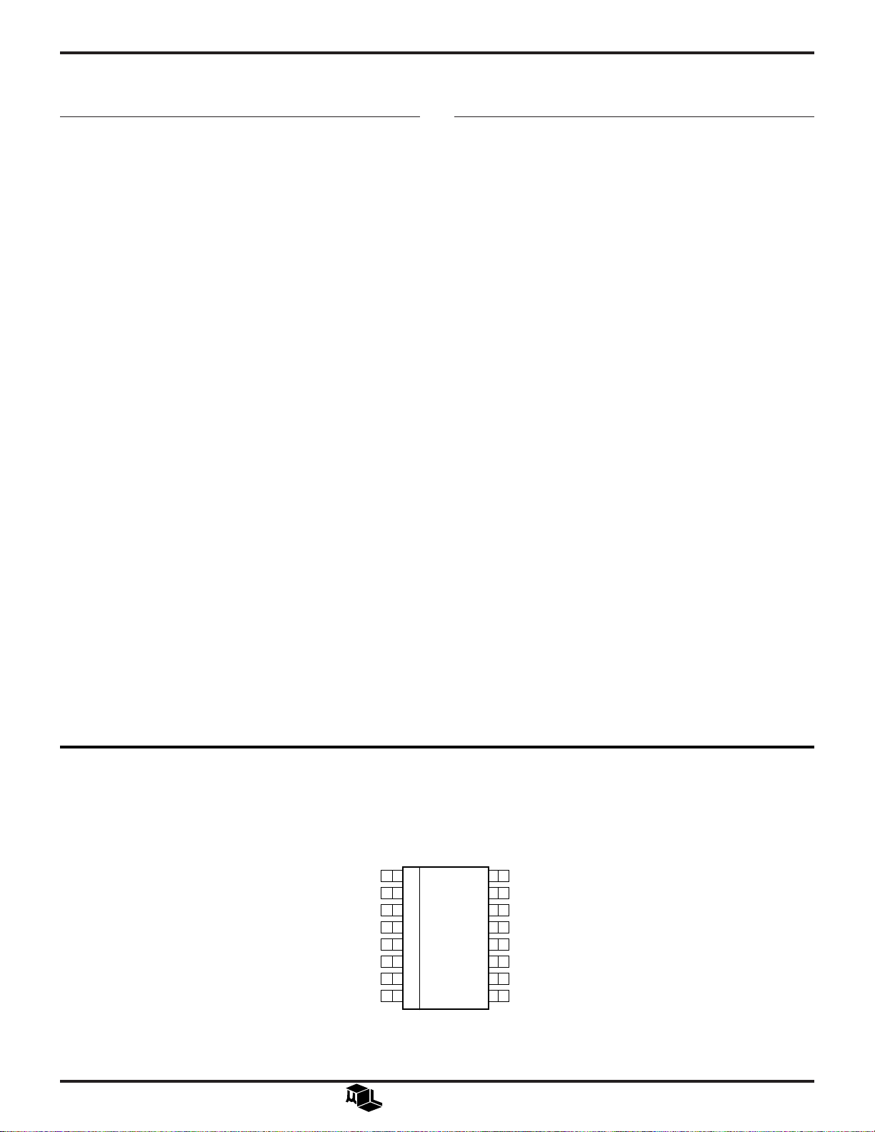
PIN CONNECTION
2
ML6622
16-Pin Narrow SOIC (S16N)
ENABLE
LINKLED
V
ECL OUT+
ECL OUT–
GND
LINK+
LINK–
CC
1
2
3
4
5
6
7
8
TOP VIEW
Micro Linear
CTIMER
16
CAP
15
V
14
13
12
11
10
9
CC
V
+
IN
V
–
IN
GNDA
THIN
V
REF
A
Page 3

ML6622
ABSOLUTE MAXIMUM RATINGS
Absolute maximum ratings are those values beyond which
the device could be permanently damaged. Absolute
maximum ratings are stress ratings only and functional
device operation is not implied.
VCC....................................................... GND –0.3V to 6V
VCCA ..................................................... GND –0.3V to 6V
Inputs/Outputs .......................... GND – 0.3V to VCC + 0.3
Junction Temperature ............................................. 150°C
ELECTRICAL CHARACTERISTICS
Unless otherwise specified, VCC = V
SYMBOL PARAMETER CONDITIONS MIN TYP MAX UNITS
= 5V ± 10%, T
CC
= Operating Temperature Range. (Note 1)
A
Storage Temperature Range ...................... –65°C to 150°C
Lead Temperature (Soldering 10 sec.) ...................... 260°C
Thermal Resistance ........................................... 100°C/W
I
CC
V
REF
IV
REF
V
IN
VTH ADJ External Voltage 0.5 V
Range at THIN to set V
EN Input-referred Voltage Noise 100 MHz BW 25 µV
R
IN
I
THIN
VOL-V
VOH-V
t
r
t
f
Link Detect
AS_Max Assert Time (off to on) C
VCC Supply Current No load on ECL outputs 35 50 mA
Reference Voltage 2.30 2.47 2.57 V
V
Output Current –1 3 +5 mA
REF
Input Signal Range 3.5 1600 mV
REF
TH
Input Resistance VIN+, V
Input Bias Current of THIN –100 +100 µA
ECL Output Voltage-Low Through 50Ω to V
CC
ECL Output Voltage-High Through 50Ω to V
CC
Data Output Rise Time 0.5 1.3 ns
Data Output Fall Time 0.5 1.3 ns
TIME
– 500 770 1500 Ω
IN
–2V –1.810 –1.730 –1.620 V
CC
–2V ␣ C Suffix –1.025 –0.963 –0.800 V
CC
␣ I Suffix –1.025 –0.963 –0.780 V
= 2000pF 0 100 µs
P-P
V
RMS
ANS_Max Deassert Time (on to off) C
V
TH
BW Bandwidth 1-3dB 200 MHz
VIPW Minimum Input Pulse Width 5 ns
DCD Duty Cycle Distortion Data rate = 155Mb/s
DDJ Data Dependent Jitter FDDI – 56 Data Pattern
Note 1: Limits are guaranteed by 100% testing, sampling, or correlation with worst-case conditions.
Input threshold THIN = V
Hysteresis 1.5 1.7 2 dB
Peak-to-peak 50% duty cycle input 0.5 ns
Peak-to-peak VIN = 60mV, Data rate = 125Mb/s 1.2 ns
= 2000pF 0 350 µs
TIME
Assert 8 10 12 mV
REF
Micro Linear
3
Page 4

ML6622
Threshold Assert
V
THIN
()=
500
FUNCTIONAL DESCRIPTION
The ML6622 high speed data quantizer accepts a low
level analog signal from a pin diode and transimpedance
amp front end and converts it into digital ECL levels for
subsequent digital processing. The input signal, from a
transimpedance amplifier, is immediately amplified by a
two-stage video amplifier. The output of this amplifier
feeds two parallel paths.
The data path is comprised of a high speed comparator
that outputs PECL differential data on the ECL␣ OUT± pins.
The Link Detection path monitors the magnitude of the
amplified input signal, compares it to a user-settable
threshold, and provides the result of the comparison as a
PECL differential output on the Link± pins. The timer
following the threshold block is used to set the Link
Detect output acquire and deacquire time using a
capacitor.
AMPLIFIER
The amplifier is a two stage video amplifier with a gain of
approximately 55V/V. Maximum sensitivity is achieved
through the use of the DC restoration feedback loop and
AC coupling the input. The AC coupling input capacitors,
in conjunction with the input impedance of the amplifier,
establish a high pass filter with the lower 3dB point
determined by the input resistance and the input coupling
capacitors. This cap also adds a secondary pole to the
offset loop.
Since the amplifier has a differential input, two AC
capacitors of equal value are required. If the signal driving
the input is single ended, the other coupling capacitor
should be tied to VCC.
A low-pass filter in the offset loop is created with the
capacitor on pin 15 (CAP). The lower 3dB point
controlled by a capacitor tied from the CAP pin to V
shown in the application circuit. For stability reasons the
value of the capacitor on the CAP pin should be 10 times
larger than the input coupling capacitors. The 3dB point is
given by the following equation:
REF
as
COMPARATOR
A high speed ECL comparator with PECL outputs is used
for the quantization function. The comparator has an
Enable input pin which takes an ECL level. This Enable
pin is normally driven by LINKLED, which causes the
output to be enabled when the link is up and disabled
when the link is down. When ENABLE is low the
comparator is operational. When ENABLE is high the
comparator is disabled causing ECL OUT– to go low and
ECL OUT+ to go high. The ENABLE pin can be tied to
ground to keep the comparator permanently enabled.
LINK DETECT CIRCUIT
The Link Detection Circuit is used to accurately measure
the input amplitude to determine whether it is large
enough to reliably recover the input signal. Once the Bit
Error Rate (BER) for the ML6622 receive circuit is
determined, the link detect threshold can be set so that the
Link Detect Circuit will shut off before the error rate
exceeds the link requirement.
The Link Detection Circuit consists of three functional
blocks; Thresh, Timer, and Link Out. Thresh detects the
output of Amp and compares it to a programmable
threshold input THIN. As long as the input amptitude is
greater than the programmable threshold input, the Link
Detect output remains active.
When the peak input drops below THIN, Thresh’s output
changes state and Timer delays the Link Out state change
for a programmable amount of time. When using the
default C
and the assert time values conform to the ANSI X3.1661990 PMD standard for FDDI.
To improve stability, the Link Detect circuit includes 1.7dB
of hysteresis.
The V
REF
Link Detect threshold. For greater sensitivities, V
be divided down before applied to THIN. The formula for
the threshold on the thin pin is as follows:
capacitance of 2000pF, the deassert time
TIME
output can be tied directly to THIN to set the
can
REF
Although the input is AC coupled, the offset voltage
within the amplifier will be present at the amplifier’s
output. The removal of the dc offset in the amplifier helps
the circuit respond to small input voltages, and reduces
duty-cycle distortion. In order to reduce this error, a
negative feedback loop nulls the offset voltage. An
external capacitor connected to the CAP pin is used to
store the offset voltage. This voltage is compared to V
and a difference current proportional to the result is
applied to the negative side of the input stage of the AMP
circuit block thereby nulling the DC offset.
4
=
F
3
dB
1
2 100
××π
k
C
V
THIN
750
REF
ThresholdDeassert
()=
Micro Linear
Page 5

APPLICATION CIRCUIT
+5V
470Ω
OPTIONAL
1KΩ
+5V
1KΩ
1
ENABLE
2
LINKLED
3
V
ECL OUT+
4
ECL OUT–
5
GND
6
CC
C
TIMER
CAP
V
CC
V
IN+
V
IN–
GNDA
ML6622
16
15
A
14
13
12
11
0.1µF
V
RF+
0.01µF
V
RF–
V
RF–
0.01µF
V
RF+
LINK+
7
1KΩ
LINK–
8
1KΩ
+5V V
.1 +4.7 +4.7 .1
4.7µH
4.7µH
OPTIONAL
THIN
10
V
9
REF
RF+
V
RF–
Micro Linear
5
Page 6

ML6622
PHYSICAL DIMENSIONS inches (millimeters)
Package: S16N
16-Pin Narrow SOIC
0.386 - 0.396
16
(9.80 - 10.06)
0.017 - 0.027
(0.43 - 0.69)
(4 PLACES)
0.055 - 0.061
(1.40 - 1.55)
1
PIN 1 ID
0.050 BSC
(1.27 BSC)
0.012 - 0.020
(0.30 - 0.51)
0.148 - 0.158
(3.76 - 4.01)
0.059 - 0.069
(1.49 - 1.75)
SEATING PLANE
0.228 - 0.244
(5.79 - 6.20)
0.004 - 0.010
(0.10 - 0.26)
0º - 8º
0.015 - 0.035
(0.38 - 0.89)
0.006 - 0.010
(0.15 - 0.26)
ORDERING INFORMATION
PART NUMBER TEMPERATURE RANGE PACKAGE
ML6622CS 0° to 70°C 16-Pin Narrow SOIC (S16N)
ML6622IS–40° to 85°C16-Pin Narrow SOIC (S16N) (Obsolete)
© Micro Linear 1997 is a registered trademark of Micro Linear Corporation
Products described in this document may be covered by one or more of the following patents, U.S.: 4,897,611; 4,964,026; 5,027,116; 5,281,862; 5,283,483; 5,418,502; 5,508,570; 5,510,727; 5,523,940;
5,546,017; 5,559,470; 5,565,761; 5,592,128; 5,594,376; Japan: 2598946. Other patents are pending.
Micro Linear reserves the right to make changes to any product herein to improve reliability, function or design.
Micro Linear does not assume any liability arising out of the application or use of any product described herein,
neither does it convey any license under its patent right nor the rights of others. The circuits contained in this
data sheet are offered as possible applications only. Micro Linear makes no warranties or representations as to
whether the illustrated circuits infringe any intellectual property rights of others, and will accept no responsibility
or liability for use of any application herein. The customer is urged to consult with appropriate legal counsel
before deciding on a particular application.
6
Micro Linear
2092 Concourse Drive
San Jose, CA 95131
Tel: 408/433-5200
Fax: 408/432-0295
DS6622-01
 Loading...