

Datasheet ML65L245CK, ML65245CS, ML65L245CS, ML65245CK Datasheet (Micro Linear Corporation)
Page 1

August 1996
ML65245**/ML65L245*
High Speed Octal Buffer Transceivers
GENERAL DESCRIPTION
The ML65245 and ML65L245 are non-inverting octal
transceivers. The high operating frequency (50MHz
driving a 50pF load) and low propagation delay
(ML65245 – 1.7ns, ML65L245 – 2ns) make them ideal for
very high speed applications such as processor bus
buffering and cache and main memory control.
These transceivers use a unique analog implementation to
eliminate the delays inherent in traditional digital designs.
Schottky clamps reduce under and overshoot, and special
output driver circuits limit ground bounce. The ML65245
and ML65L245 conform to the pinout and functionality of
the industry standard FCT245 and are intended for
applications where propagation delay is critical to the
system design.
Note: This part was previously numbered ML6580.
BLOCK DIAGRAM
FEATURES
■ Low propagation delay — 1.7ns ML65245
2.0ns ML65L245
■ Fast 8-bit TTL level transceiver with three-state
capability on the output
■ TTL compatible input and output levels
■ Schottky diode clamps on all inputs to handle
undershoot and overshoot
■ Onboard schottky diodes minimize noise
■ Reduced output swing of 0 – 4.1 volts
■ Ground bounce controlled outputs, typically less
than 400mV
■ Industry standard FCT245 type pinout
■ Applications include high speed cache memory, main
memory, processor bus buffering, and graphics cards
** This Product Is End Of Life As Of August 1, 2000
* This Product Is Obsolete
T/R
OE
V
CC
A0
20
2
V
CC
1
19
18
10
GND
B0
A1
3
17
B1
A2
16
B2
A3
4
5
15
B3
A4
6
14
B4
A5
13
B5
A6
7
8
12
B6
A7
9
11
B7
1
Page 2
ML65245**/ML65L245*
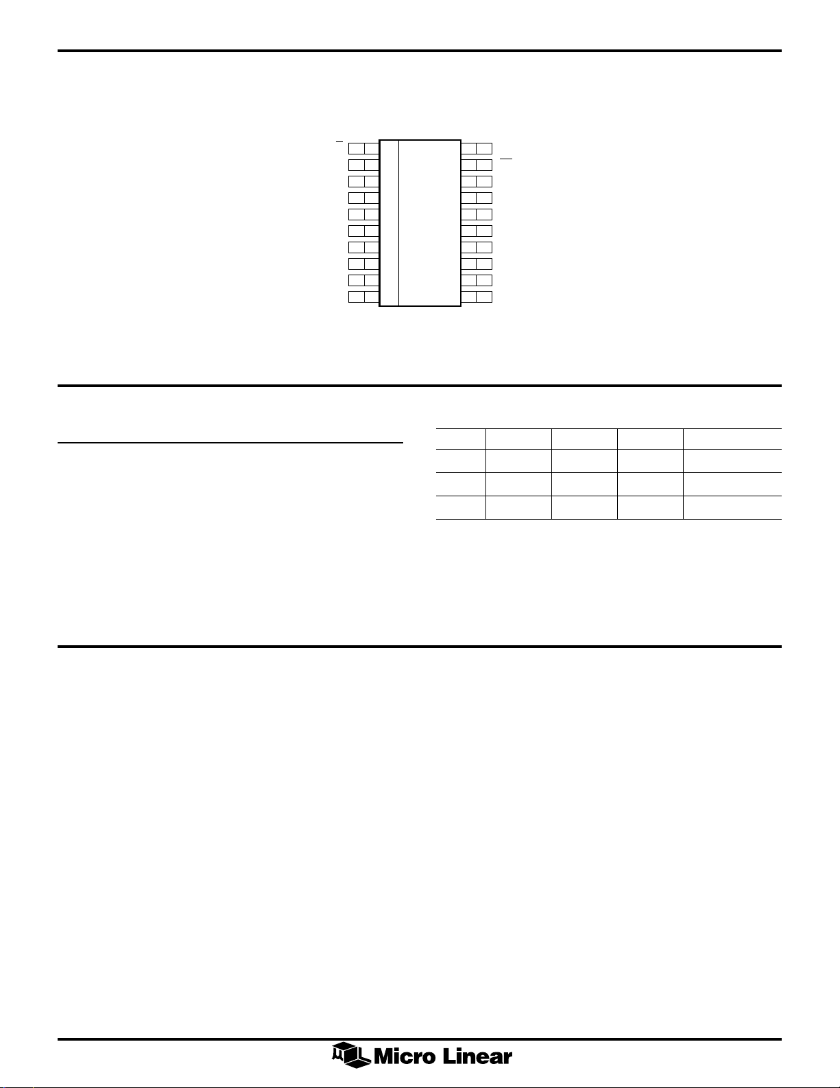
PIN CONFIGURATION
20-Pin SOIC, QSOP
PIN DESCRIPTION
NAME I/O DESCRIPTION
Ai I/O Data Bus A
Bi I/O Data Bus B
T/R I Direction select
OE I Output Enable
GND I Signal Ground
V
CC
I + 5V supply
T/R
GND
A0
A1
A2
A3
A4
A5
A6
A7
1
2
3
4
5
6
7
8
9
10
TOP VIEW
20
19
18
17
16
15
14
13
12
11
V
OE
B0
B1
B2
B3
B4
B5
B6
B7
CC
FUNCTION TABLE
OE T/R A B Function
H X Z Z Disable
L L Output Input Bus B to Bus A
L H Input Output Bus A to Bus B
L = Logic Low
H = Logic High
X = Don’t Care
Z = High Impedance
ABSOLUTE MAXIMUM RATINGS
V
................................................................................ –0.3V to 7V
CC
DC Input voltage ............................. –0.3V to VCC + 0.3V
AC Input voltage (< 20ns) ....................................... –3.0V
DC Output voltage .......................... –0.3V to VCC + 0.3V
Output sink current (per pin) ................................ 120mA
Storage temperature ................................ –65°C to 150°C
Junction temperature ............................................. 150°C
Thermal Impedance (qJA)
SOIC ...............................................................96°C/W
QSOP ............................................................ 100°C/W
2
Page 3
ML65245**/ML65L245*
ELECTRICAL CHARACTERISTICS
Unless otherwise stated, these specifications apply for: VCC = 5.0 ± 5%V, TA = 0°C to 70°C (Note 1)
SYMBOL PARAMETER CONDITIONS MIN TYP MAX UNITS
AC ELECTRICAL CHARACTERISTICS (C
t
PLH
, t
Propagation delay Ai to/from Bi (Note 2) ML65245 1.4 1.7 ns
PHL
LOAD
= 50pF, R
LOAD
= 500ý)
ML65L245 1.6 2.0 ns
t
t
OE
OD
Output enable time 10 15 ns
OE, T/R to Ai/Bi
Output disable time 10 ns
OE, T/R to Ai/Bi
C
IN
DC ELECTRICAL CHARACTERISTICS (unless otherwise stated C
V
IH
V
I
IH
Input Capacitance 8 pF
LOAD
= 50pF, R
LOAD
= )
Input high voltage Logic HIGH 2.0 V
Input low voltage Logic LOW 0.8 V
IL
Input high current Per pin, VIN = 3V ML65245 0.5 1.5 mA
ML65L245 0.3 0.5 mA
I
IL
Input low current Per pin, VIN = 0V ML65245 2.4 3.5 mA
ML65L245 0.8 1.0 mA
I
HI-Z
Three-state output current VCC = 5.25V, 0 < V
IN
< V
CC
5µA
IOSShort circuit current VCC = 5.25V, VO = GND –60 –225 mA
(Note 3)
V
IC
V
OH
Input clamp voltage VCC = 4.75V, IIN = 18mA –0.7 –1.2 V
Output high voltage VCC = 4.75V, IOH = 100µA 2.4 V
(Notes 4 & 5)
V
OL
Output low voltage V
= 4.75V, IOL = 25mA 0.6 V
CC
(Notes 4 & 5)
V
OFF
VIN – V
per buffer VCC = 4.75V (Note 4) ML65245 0 100 200 mV
OUT
ML65L245 0 200 300 mV
I
CC
Quiescent Power VCC = 5.25V, f = 0Hz, 55 80 mA
Supply Current Inputs/outputs open
Note 1: Limits are guaranteed by 100% testing, sampling or correlation with worst case test conditions.
Note 2: One line switching, see Figure 3, t
Note 3: Not more than one output should be shorted for more than a second.
Note 4: This is a true analog buffer. In the linear region, the output tracks the input with an offset (V
Note 5: See Figure 2 for IOH versus VOH and IOL versus VOL data.
= 2.6V for the ML65245 and 2.7 for the ML65L425. V
V
IN
PLH
, t
PHL
versus CL.
INPUT
OUTPUT
OH MIN
3V
0V
3V
0V
includes V
1.5V
1.5V
. For VOL, VIN = 0V, V
OFF
OFF
1.5V
t
PLH
). For VOH, VIN = 2.7V.
tR, tF ≤ 4ns
1.5V
OL MAX
t
PHL
includes V
OFF
3
Page 4

ML65245**/ML65L245*
CH1 1.00V CH2 1.00V 10.0ns CH1 1.00V CH2 1.00V 10.0ns
(mA)
OL
I
(ns)
pd
t
220
200
180
160
140
120
100
3.0
2.5
2.0
1.5
1.0
0.5
74FCT245
ML65245
Figure 1. Ground Bounce Comparison, Four Outputs Switching into 50pF Loads.
+20
0
–20
–40
–60
–80
(mA)
OH
I
–100
80
60
40
20
0
0.0
0.5 1.0 1.5 2.0
V
(V)
OL
Figure 2a. Typical VOL Versus I
2.5
OL
for One Buffer Output.
ML65L245
ML65245
–120
–140
–160
–180
–200
210
190
170
150
(mA)
130
CC
I
110
2.5
Figure 2b. Typical VOH Versus I
3.0 3.5 4.0
V
(V)
OH
OH
for One Buffer Output.
150pF
100pF
75pF
90
70
50pF
30pF
0.0
50 75 150
LOAD CAPACITANCE (pF)
Figure 3. Propagation Delay (t
Capacitance, One Output Switching.
4
PLH
10030
, t
) Versus Load
PHL
50
20 30 40 50 60 70 80 90
10
FREQUENCY (MHz)
Figure 4. ICC Versus Frequency for Various Load
Capacitances, Four Outputs Switching.
Page 5

ML65245**/ML65L245*
FUNCTIONAL DESCRIPTION
The ML65245 and ML65L245 are very high speed noninverting transceivers with three-state outputs which are
ideally suited for bus-oriented applications. They provide
a low propagation delay by using an analog design
approach (a high speed unity gain buffer), as compared to
conventional digital approaches. The ML65245 and
ML65L245 follow the pinout and functionality of the
industry standard FCT245 series of transceivers and are
intended to replace them in designs where the
propagation delay is a critical part of the system design
considerations. The ML65245 and ML65L245 are capable
of driving load capacitances several times larger than their
input capacitance. They are configured so that signals
pass from Ai to Bi, or from Bi to Ai, depending on the state
of the T/R pin. All of the signal lines can be made high
impedance via the OE pin.
These unity gain analog buffers achieve low propagation
delays by having the output follow the input with a small
offset. The output rise and fall times will closely match
those of the input waveform. All inputs and outputs have
Schottky clamp diodes to handle undershoot or overshoot
noise suppression in unterminated applications. All
outputs have ground bounce suppression (typically
< 400mV), high drive output capability with almost
immediate response to the input signal, and low output
skew.
The IOL current drive capability of a buffer/line driver is
often interpreted as a measure of its ability to sink current
in a dynamic sense. This may be true for CMOS buffer/
line drivers, but it is not true for the ML65245 and
ML65L245. This is because the their sink and source
current capability depends on the voltage difference
between the output and the input. The ML65245 can sink
or source more than 100mA to a load when the load is
switching due to the fact that during the transition, the
difference between the input and output is large. IOL is
only significant as a DC specification, and is 25mA.
ARCHITECTURAL DESCRIPTION
Until now, buffer/line drivers have been implemented in
CMOS logic and made to be TTL compatible by sizing the
input devices appropriately. In order to buffer large
capacitances with CMOS logic, it is necessary to cascade
an even number of inverters, each successive inverter
larger than the preceding, eventually leading to an inverter
that will drive the required load capacitance at the
required frequency. Each inverter stage represents an
additional delay in the gating process because in order for
a single gate to switch, the input must slew more than half
of the supply voltage. The best of these CMOS buffers has
managed to drive a 50pF load capacitance with a delay of
3.2ns. Micro Linear has produced an octal transceiver
with a delay less than 1.7ns by using a unique circuit
architecture that does not require cascaded logic gates.
The ML65245 uses a feedback technique to produce an
output that follows the input. If the output voltage is not
close to the input, then the feedback circuitry will source
or sink enough current to the load capacitance to correct
the discrepancy.
VCC
R8
Q1
R3
R1
IN OUT
Q4
Q3
GND
R4
R2
Q6
Q5
R6R5
Q2
R7
Q7
Figure 5. One buffer cell of the ML65245
5
Page 6

ML65245**/ML65L245*
The basic architecture of the ML65245 is shown in Figure
5. It is implemented on a 1.5µm BiCMOS process.
However, in this particular circuit, all of the active devices
are NPNs — the fastest devices available in the process.
In this circuit, there are two paths to the output. One path
sources current to the load capacitance when the signal is
asserted, and the other path sinks current from the output
when the signal is negated.
The assertion path is the emitter follower path consisting
of the level shift transistor Q1, the output transistor Q2,
and the bias resistor R8. It sources current to the output
through the 75ý resistor R7 which is bypassed by another
NPN (not shown) during fast input transients. The
negation path is a current differencing op amp connected
in a follower configuration. The active components in this
amplifier are transistors Q3-Q7. R3-R6 are bias resistors,
and R1 and R2 are the feedback resistors. The key to
understanding the operation of the current differencing op
amp is to know that the currents in transistors Q3 and Q5
are the same at all times and that the voltages at the bases
of Q4 and Q6 are roughly the same. If the output is higher
than the input, then an error current will flow through R2.
This error current will flow into the base of Q6 and be
multiplied by b squared to the collector of Q7, closing the
loop. The larger the discrepancy between the output and
input, the larger the feedback current, and the harder Q7
sinks current from the load capacitor.
A number of MOSFETs are not shown in Figure 5. These
MOSFETs are used to three-state dormant buffers. For
instance, the feedback resistors R1 and R2 were
implemented as resistive transmission gates to ensure that
disabled buffers do not load the lines they are connected
to. Similarly, there is a PMOS in series with R8 that is
normally on but shuts off for disable. Other MOSFETs
have been included to ensure that disabled buffers
consume no power.
TERMINATION
R7 in Figure 5 also acts as a termination resistor. This 75ý
resistor is in series with the output and therefore helps
suppress noise caused by transmission line effects such as
reflections from mismatched impedances. System
designers using CMOS transceivers commonly have to use
external resistors in series with each transceiver output to
suppress this noise. Systems using the ML65245 or
ML65L245 may not have to use these external resistors.
APPLICATIONS
There are a wide variety of needs for extremely fast buffers
in high speed processor system designs like Pentium,
PowerPC, Mips, Sparc, Alpha and other RISC processors.
These applications are either in the cache memory area or
the main memory (DRAM) area. In addition, fast buffers
find applications in high speed graphics and multimedia
applications. The high capacitive loading due to
multiplexed address lines on the system bus demand
external buffers to take up the excess drive current. The
needed current to skew the transitions between rise and
fall times must be done without adding excessive
propagation delay. The ML65245 and ML65L245 are
equipped with Schottky diodes to clean up ringing from
overshoot and undershoot caused by reflections in
unterminated board traces.
BUFFERING MAIN MEMORY
An example main memory application for the Intel PCI
chipset with the Pentium processor is shown in Figure 6.
This is only intended as a general reference. For details
please refer to the appropriate Intel documentation. This
system has a 66MHz host processor and a 33MHz main
(DRAM) memory bus. The main memory row and column
addresses (RAS & CAS) and write enable (WE) signals are
provided by the PCMC chip (PCI Cache and Memory
Controller) device. The DRAM SIIMMs put a heavy load
on the PCMC and must be buffered. Three buffered copies
of the address signals and write enable are required to
drive the six row array. The ML65245 provides the
buffered signals and gives extra margin to be able to use
slower memory modules instead of the normally required
50/70ns. The burst read (page-hit) performance is typically
7-4-4-4 at 66MHz for 70ns DRAMs or 6-3-3-3 at 66MHz
for 50ns DRAMs. This usually translates to significantly
higher costs. With the speed improvement offered by the
ML65245, a 6-3-3-3 burst with 60ns DRAMs may be
achievable. The extra margin comes from the 1.5ns
propagation delay of the buffer. External resistor arrays are
not necessary. This becomes even more of an issue in
future PCI systems which may operate at 80MHz and
beyond.
This kind of main memory application for the ML65245
could potentially extend to other kinds of processor
systems which do not require latched buffering. Figure 7
shows a main memory design example with the ML65245
for the Mips R4X00 RISC processor based system without
secondary cache. The faster propagation delay essentially
translates to a faster main memory access.
6
Page 7

ML65245**/ML65L245*
LATCH
WE
MAddr
CONTROL
ADDRESS/DATA
CNTL
CACHE
(SRAM)
PCMC
CONTROL
ADDRESS
DATA
LBX
MAIN MEMORY
DATA
66 MHz
Pentium™ Processor
(DRAM)
LOCAL BUS
BWE
BMAddr
PCI™ BUS (33 MHz)
ML65245 BUFFER
LBX CNTL
Figure 6. ML65245 in a main memory application for a Pentium based system. The high drive and low propagation
delay are essential to buffer the write enable and memory addresses to the main memory SIIMMs.
CONTROL
CDRAM
or
DRAM
R4X00™
150/75 MHz
ML65245
CONTROL
ADDRESS/DATA
CDRAM
or
DRAM
ML65245
ADDR
ML65245
MEMORY I/O
CONTROLLER
Figure 7. The ML65245 in a non-cache, main memory RISC application. The main memory could be DRAM or
Cache DRAM. The ML65245 can be used as a data I/O transceiver as well as an address buffer, as shown above.
7
Page 8

ML65245**/ML65L245*
APPLICATION 2
BUFFERING CACHE MEMORY
With the advent of higher power operating systems like
Windows NT, NeXT Step, Windows, OS/2 Warp, etc.,
RISC processor designs such as the Mips R4000 series are
gaining momentum. In these systems the interface to
secondary cache has a critical path in the address and bus
control pins. As shown in Figure 8, any propagation delay
time saved in the buffer translates to a slower SRAM
access requirement and is therefore less expensive.
Currently, the secondary cache bus operates at 75MHz.
R4X00
150/75 MHz
ADDR
OE
CS
ML65245
In order to meet the 13ns cycle time, the SRAM and buffer
must meet a total access time of 12ns. With the ML65245,
the required SRAM access time is 10ns at 75MHz and
18ns at 50MHz. With the fastest FCT buffer available
(3.2ns), the SRAM access time required in the above
scenarios would be 8ns and 15ns respectively. This access
time difference could mean the difference between using
expensive BiCMOS SRAMs versus less expensive CMOS
SRAMs.
SRAM
10ns
SRAM
10ns
DATA BUS
SECONDARY CACHE MODULE
Figure 8. ML65245 in a R4X00 secondary cache application. The address and control signal path is critical and
loads the R4X00 output pins. The ML65245 buffer alleviates the load on the R4X00 and because it is fast,
slower, less expensive SRAMs can be used.
ADDR
WE
DATA
ADDR1
t
A
t
H
Figure 9. Timing waveform showing address buffer switching rate (tA + tH) in a secondary cache module.
8
Page 9

PHYSICAL DIMENSIONS inches (millimeters)
Package: K20
20-Pin QSOP
0.338 - 0.348
(8.58 - 8.84)
20
ML65245**/ML65L245*
Package: K20
20-Pin QSOP
0.050 - 0.055
(1.27 - 1.40)
(4 PLACES)
0.055 - 0.061
(1.40 - 1.55)
20
PIN 1 ID
1
0.025 BSC
(0.63 BSC)
0.008 - 0.012
(0.20 - 0.31)
0.498 - 0.512
(12.65 - 13.00)
0.150 - 0.160
(3.81 - 4.06)
0.060 - 0.068
(1.52 - 1.73)
SEATING PLANE
Package: S20
20-Pin SOIC
0.228 - 0.244
(5.79 - 6.20)
0.004 - 0.010
(0.10 - 0.26)
Package: S20
20-Pin SOIC
0º - 8º
0.015 - 0.035
(0.38 - 0.89)
0.006 - 0.010
(0.15 - 0.26)
0.024 - 0.034
(0.61 - 0.86)
(4 PLACES)
0.090 - 0.094
(2.28 - 2.39)
0.291 - 0.301
0.398 - 0.412
(7.39 - 7.65)
(10.11 - 10.47)
PIN 1 ID
1
0.050 BSC
(1.27 BSC)
0.012 - 0.020
(0.30 - 0.51)
0.095 - 0.107
(2.41 - 2.72)
SEATING PLANE
0.005 - 0.013
(0.13 - 0.33)
0º - 8º
0.022 - 0.042
(0.56 - 1.07)
0.007 - 0.015
(0.18 - 0.38)
9
Page 10

ML65245**/ML65L245*
ORDERING INFORMATION
PART NUMBER SPEED TEMPERATURE RANGE PACKAGE
ML65245CK (EOL) 1.7ns 0°C to 70°C 20-Pin QSOP (K20)
ML65245CS (EOL) 1.7ns 0°C to 70°C 20-Pin SOIC (S20)
ML65L245CK (Obsolete) 2.0 0°C to 70°C 20-Pin QSOP (K20)
ML65L245CS (Obsolete) 2.0 0°C to 70°C 20-Pin SOIC (S20)
Intel, Pentium, PCI are registered trademarks of Intel Corporation. Mips, Alpha and Sparc are registered trademarks of Silicon Graphics, DEC and
Sun Microsystems respectively.
© Micro Linear 1996 is a registered trademark of Micro Linear Corporation
Products described in this document may be covered by one or more of the following patents: 4,897,611; 4,964,026; 5,027,116;
5,281,862; 5,283,483; 5,418,502; 5,508,570; 5,510,727; 5,523,940; 5,546,017. Other patents are pending.
Micro Linear reserves the right to make changes to any product herein to improve reliability, function or design.
Micro Linear does not assume any liability arising out of the application or use of any product described herein,
neither does it convey any license under its patent right nor the rights of others. The circuits contained in this
data sheet are offered as possible applications only. Micro Linear makes no warranties or representations as to
whether the illustrated circuits infringe any intellectual property rights of others, and will accept no responsibility
or liability for use of any application herein. The customer is urged to consult with appropriate legal counsel
before deciding on a particular application.
2092 Concourse Drive
10
San Jose, CA 95131
Tel: 408/433-5200
Fax: 408/432-0295
DS65245-01
 Loading...